1. Introduction
In sectors such as aerospace, energy, and transportation, damage initiated on the surface of metal components tends to propagate when subjected to loading during service. This degradation in mechanical properties may even culminate in sudden fracture, posing a significant threat to the safety and operational reliability of the equipment. Therefore, non-destructive testing (NDT) techniques are crucial for ensuring the integrity of these critical components [
1,
2,
3].
Eddy current testing (ECT) is an efficient electromagnetic NDT technique based on Faraday’s law of electromagnetic induction: an excitation coil generates an alternating magnetic field that induces eddy currents in conductive materials [
4,
5,
6]. Defects distort these currents, subsequently detected by monitoring impedance variations in a sensing coil. This technique offers advantages including non-contact inspection, high surface defect sensitivity, and couplant-free operation. ECT is widely applied for crack detection in aero-engine blades, corrosion monitoring in nuclear piping, fatigue assessment in railway components, and real-time quality inspection in metal manufacturing [
7]. Its non-contact nature and exceptional surface sensitivity establish ECT as an indispensable technology within industrial safety assurance frameworks [
8].
A key limitation of current ECT systems is the susceptibility of defect-induced voltage perturbations to being overwhelmed by complex noise, encompassing probe lift-off fluctuations, material microstructural inhomogeneity, and environmental electromagnetic interference [
9,
10]. Traditional signal processing methods (such as FT and peak detection) exhibit significant limitations [
11]: they struggle to effectively separate weak damage features that overlap in the frequency domain, their ability to suppress non-stationary noise is inadequate, and they incur substantial errors when quantifying minute voltage variations. Consequently, the reliability of identifying and quantifying weak damage signals is significantly reduced. In industrial environments with high noise levels, defect detection rates and quantification accuracy degrade significantly [
12,
13].
In recent years, with the continuous advancement of signal processing technologies, many novel algorithms have emerged, such as wavelet transform (WT) [
14,
15,
16,
17,
18], adaptive filters [
19,
20,
21], and machine learning [
14,
22,
23,
24], which effectively overcome the limitations of traditional methods in noise suppression, signal analysis, and feature extraction. Among these, the WT, with its multi-resolution analysis capability, enables analysis of signals at different scales, allowing for precise extraction of local features within the signal. Particularly in processing signals with transient changes and non-stationary characteristics, DWT demonstrates excellent performance, as it can adaptively decompose signals in both the time and frequency domains, overcoming the limitations of the Fourier Transform in handling instantaneous variations. The innovation of this study lies in the proposal of an eddy current testing system that integrates a discrete wavelet transform (DWT) with an FPGA hardware platform, enabling efficient real-time processing of complex eddy current signals. Compared to traditional time-domain and frequency-domain methods, this system leverages the advantages of multi-resolution analysis provided by the wavelet transform, allowing for accurate defect feature extraction in high-noise environments, significantly improving the signal-to-noise ratio (SNR) and reducing errors in quantifying minute voltage variations. Furthermore, through the hardware implementation on an FPGA, the system meets the real-time detection requirements in industrial applications, overcoming the computational complexity and slow response times associated with traditional algorithms.
This paper designs a non-destructive ECT system based on the DWT for detecting metal surface damage. The system employs a Direct Digital Synthesizer (DDS) to generate high-frequency excitation signals, which are then output to the probe. The output signal from the probe is conditioned, acquired by an FPGA, and subsequently transmitted to the host computer. The DWT is applied to the signals received by the host computer to extract defect information accurately. The structure of this paper is organized as follows:
Section 2 details the design of the system’s hardware architecture.
Section 3 describes the signal processing algorithms employed in the system.
Section 4 presents experiments conducted on the proposed system to validate its capability for detecting metal surface damage. Finally,
Section 5 provides the conclusions of this paper.
2. Hardware Circuit Design
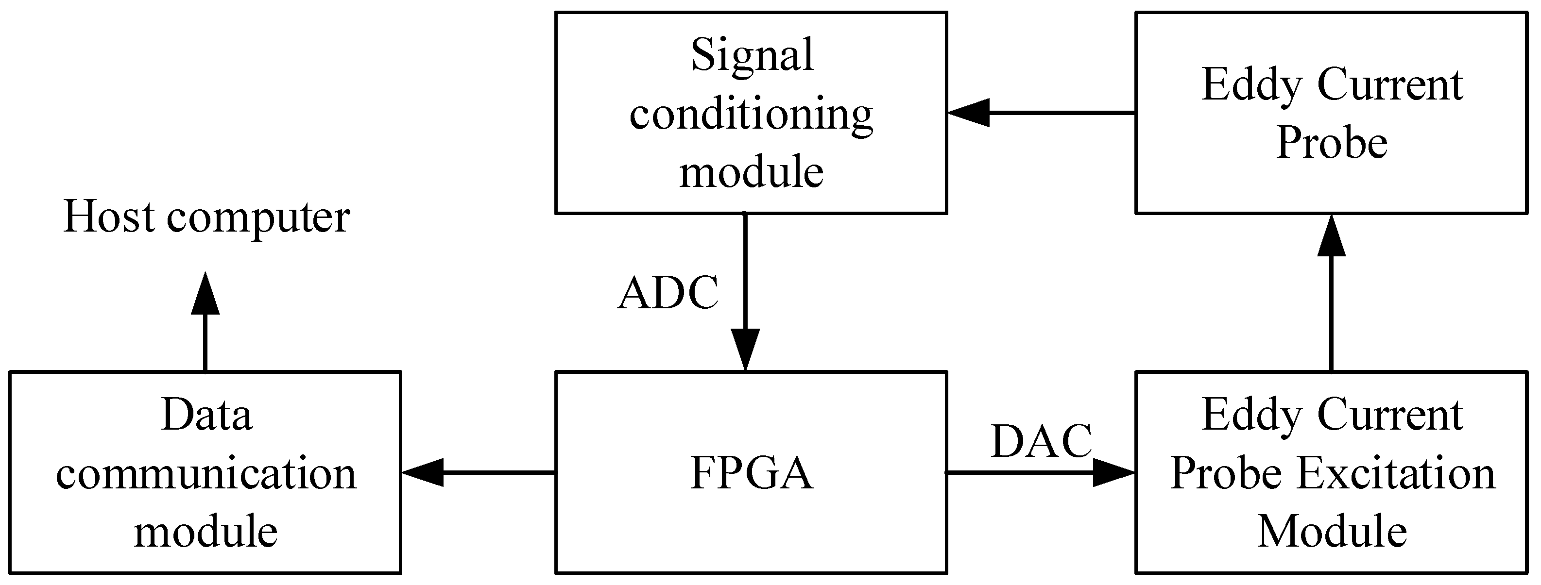
The system consists of two main parts: a dedicated hardware architecture—which includes an excitation module, signal conditioning circuit, analog-to-digital converter (ADC), and an FPGA-based processing unit—and the corresponding signal processing algorithms, as shown in
Figure 1. This section details the hardware circuit design, which is composed of an FPGA control module, a probe excitation module, a signal conditioning module, and a data communication module. Specifically, the FPGA module regulates the probe excitation frequency via a DDS, supplies reference signals to the signal conditioning module, and drives the ADC and DAC. The probe excitation module is designed with high current-driving capability to support stable excitation at MHz-level frequencies for the eddy current probe. The signal conditioning module features high sensitivity and resolution, demodulating and filtering the probe output signals. The data communication module handles transmitting the acquired data to the host computer.
The control chip for the hardware architecture employs an Altera Cyclone IV E series FPGA (model EP4CE22E22C8). DDS technology directly generates target waveforms with specific frequencies and initial phases by reading single-cycle waveform samples stored in ROM. Here, the frequency is set by the frequency control word, while the initial phase is determined by the phase control word. This system utilizes the DDS to generate a 1 MHz high-precision sinusoidal signal to drive the eddy current probe. This sinusoidal signal is converted by a 14 bit dual-channel DAC (AD9767, update rate 125 MSPS) and then drives the eddy current probe through a power amplifier with a gain of 12 dB.
Figure 2 illustrates the power amplification circuit composed of two parallel-connected operational amplifiers. This design aims to enhance the output current driving capability of the excitation signal used in the eddy current testing system. In this configuration, two identical op-amps are employed with their non-inverting inputs connected to the same excitation signal source, ensuring phase and amplitude consistency. Each op-amp output is routed through a low-value isolation resistor before being combined at the output node. These resistors serve two critical functions: they balance the output current between the two amplifiers, and suppress potential high-frequency oscillations due to slight mismatches in gain or phase.
A high-frequency alternating excitation signal in the probe’s excitation coil generates an alternating magnetic field, which induces eddy currents in the surface of the material under test. When the probe approaches a conductive metal surface or a near-surface defect, the defect perturbs the eddy current distribution. This perturbation causes a change in the impedance of the detection coil, thereby providing information about the defect. As shown in
Figure 3, the probe’s output signal is first subjected to IQ demodulation by the AD8333 chip. Subsequently, it is processed sequentially through a current-to-voltage conversion circuit and a low-pass filter. The processed signal is then acquired and transmitted to the FPGA by two AD7767 Analog-to-Digital Converters. This ADC features a single-channel design, 24 bit resolution, a sampling rate of 128 kSPS, and a voltage resolution of 0.298 μV.
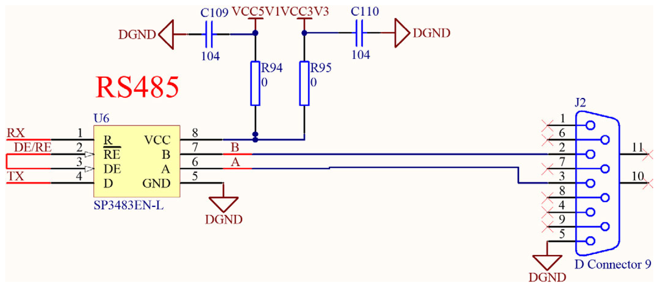
The acquired signals containing defect responses are transmitted to the host computer via an SP3483EN transceiver, operating at a data update rate of 4.5 kHz. Subsequently, digital signal processing is applied to the signals received by the host computer to achieve defect identification, as illustrated in
Figure 4.
3. Signal Processing Algorithms
Existing signal processing algorithms are broadly classified into two categories regarding the acquired output signals containing defect responses: frequency-domain and time-domain methods. Time-domain processing methods typically employ a low-pass filter to remove the signal’s high-frequency components (including high-frequency noise and defect responses). The residual between the original and filtered signals is then calculated to locate defect positions. This approach generally yields satisfactory results.
Frequency-domain processing methods commonly employ the Fourier Transform (FT), which converts the signal from the time domain to the frequency domain, revealing its global spectral energy distribution. However, the Fourier Transform is suitable only for analyzing stationary signals; its inability to provide temporal localization information for frequency components makes it difficult for this method to locate defect positions accurately.
The Short-Time Fourier Transform (STFT) generates a time-frequency joint distribution by applying a window function to the signal and performing the Fourier Transform on segmented portions. This method is suitable for analyzing non-stationary signals exhibiting slow frequency variations. However, its fixed window length leads to a fundamental trade-off between time resolution and frequency resolution (governed by the Heisenberg uncertainty principle): broader windows enhance frequency resolution (suited for analyzing low-frequency, slowly varying signals) but degrade time resolution; conversely, narrower windows improve time resolution (suited for capturing high-frequency transient signals) but sacrifice frequency resolution.
Consequently, FT and STFT are inherently limited in processing complex, non-stationary output signals typical of ECT, often leading to inaccurate defect localization.
By leveraging its multi-resolution analysis, adaptive time-frequency localization, and compact support in the energy domain, the DWT effectively overcomes the limitations inherent in both FT and STFT. It demonstrates distinct advantages for signal feature extraction and noise suppression, making it particularly well suited for processing non-stationary signals encountered in eddy current testing [
25]. Therefore, the eddy current testing system presented in this study employs DWT for defect information identification.
The core principle of DWT is implemented via a filter bank: the signal is filtered and subjected to two-fold downsampling using a low-pass filter and a high-pass filter [
26]. This process is performed iteratively across multiple levels to extract multi-scale approximation coefficients and detail coefficients. Supporting single-level or multi-level decomposition, this transform effectively separates the low-frequency approximation components from the high-frequency detail components of a signal. In eddy current testing, the electrical response characteristics of surface defects on metals are predominantly concentrated within the high-frequency detail coefficients.
This algorithm is based on the DWT for multi-level decomposition of the input signal, and is divided into the following steps:
The output signal from the eddy current probe is processed by the signal conditioning module, then converted into a digital signal by the Analog-to-Digital Converter (ADC) and input into the FPGA as the input signal.
- 2.
Choose the wavelet function:
This system utilizes the Haar wavelet as its kernel function. As the simplest member (db1) of the Daubechies wavelet family, the Haar wavelet is distinguished by its compact support, orthogonality, and high computational efficiency. Its discontinuous rectangular pulse waveform and symmetric properties facilitate rapid feature extraction. Its mathematical expressions are defined as follows:
where employing the Haar wavelet, the filter bank length is
L = 2. Given an input signal
S[
n], the algorithmic procedure for decomposition at level
j unfolds as follows:
The signal is convolved:
where
and
represent the low-pass and high-pass filter coefficients, respectively.
- 4.
Two-fold downsampling operation
The convolution results conv
h and conv
g undergo two-fold downsampling (i.e., uniform sampling retaining even-indexed samples):
where
aj[
k] denotes the
k-th low-frequency approximation coefficient at level
j, and
dj[
k] represents the
k-th high-frequency detail coefficient at level
j.
- 5.
Iterative decomposition
Take the resulting approximation coefficient sequence aj[k] as the new input signal Sn[k]. Repeat Steps 1 and 2 to perform decomposition at the next level (j + 1) until the predetermined decomposition level is reached.
- 6.
Output results
Finally, output the multi-level decomposition results of the signal, which include all the approximation and detail coefficients at each level:
These coefficients serve as the basis for subsequent signal analysis and defect characterization procedures.
In a single-level decomposition, the approximation coefficients a1 and detail coefficients d1 have a length equal to half of the original signal. Here, d1 contains the high-frequency components of the signal (such as noise and defect responses). For multi-level decomposition, the approximation coefficient sequence obtained from the previous level is iteratively processed as the new input signal. After j levels of decomposition, the DWT output comprises the detail coefficient sequences d1, d2,… dj from all levels and the final-level approximation coefficient sequence aj. This transformation process can be implemented on an FPGA (to meet real-time requirements) or on the host computer.
4. Experiment
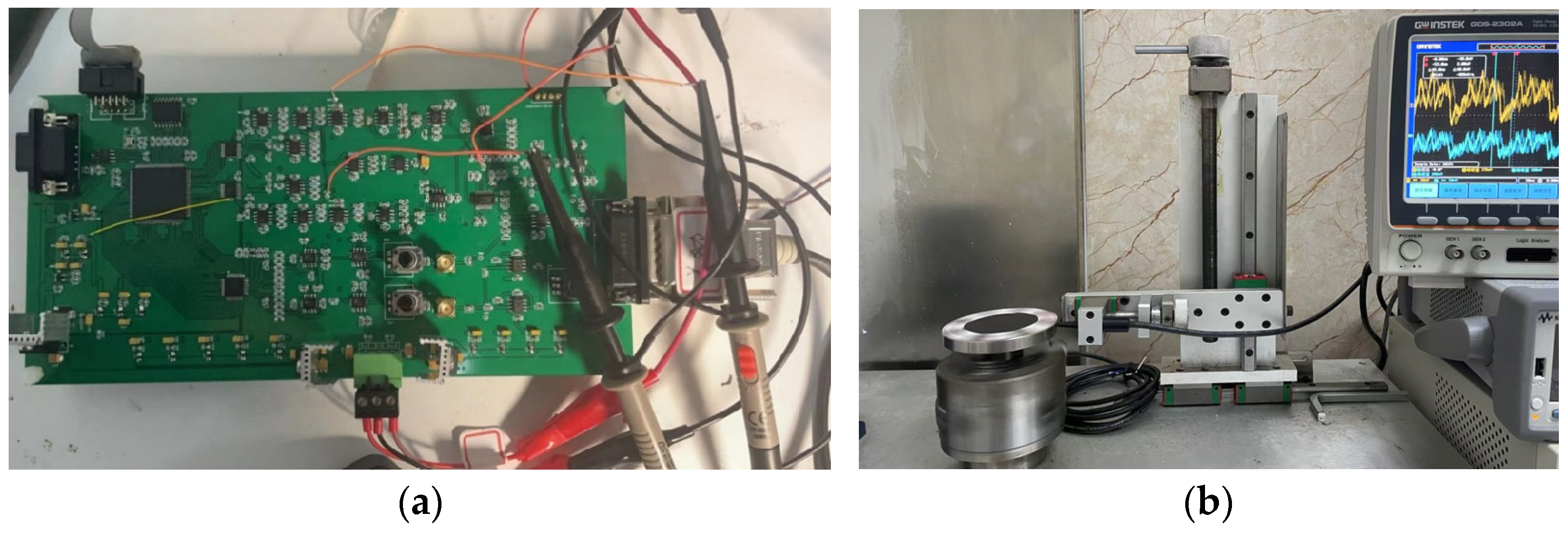
Figure 5 displays the physical photograph of the eddy current testing system designed in this study. The system is powered by a DC power supply and operates at voltages of ±12 V and GND. In the experimental setup, the eddy current probe was positioned at a fixed location, while the metallic specimen—an aluminum alloy disk containing a machined 1 mm-deep surface notch—was mounted on a horizontal translation platform. The lift-off distance between the probe and the specimen surface was precisely maintained at 0.5 mm using an adjustable micro-positioning mechanism. The excitation signal, generated by the DDS module, had a frequency of 1 MHz and an amplitude of 2.3 Vpp. During testing, the specimen was moved laterally to align or misalign the defect with the center of the probe, allowing for the acquisition of both defect and baseline signals. These measurement conditions were kept consistent throughout the experiments to ensure data reliability and repeatability.
The test specimen used in this experiment was a 1060-grade aluminum alloy disk with a diameter of 80 mm and a thickness of 10 mm. The aluminum alloy features a high purity (Al ≥ 99.6%), exhibits an electrical conductivity of approximately 3.5 × 10⁷ S/m, and is considered non-magnetic with a relative magnetic permeability close to 1. A surface defect was introduced in the form of a precisely machined rectangular notch with a width of 0.2 mm and a depth of 1 mm. The specimen surface was kept free from coatings or oxide layers to ensure reliable eddy current penetration and signal consistency.
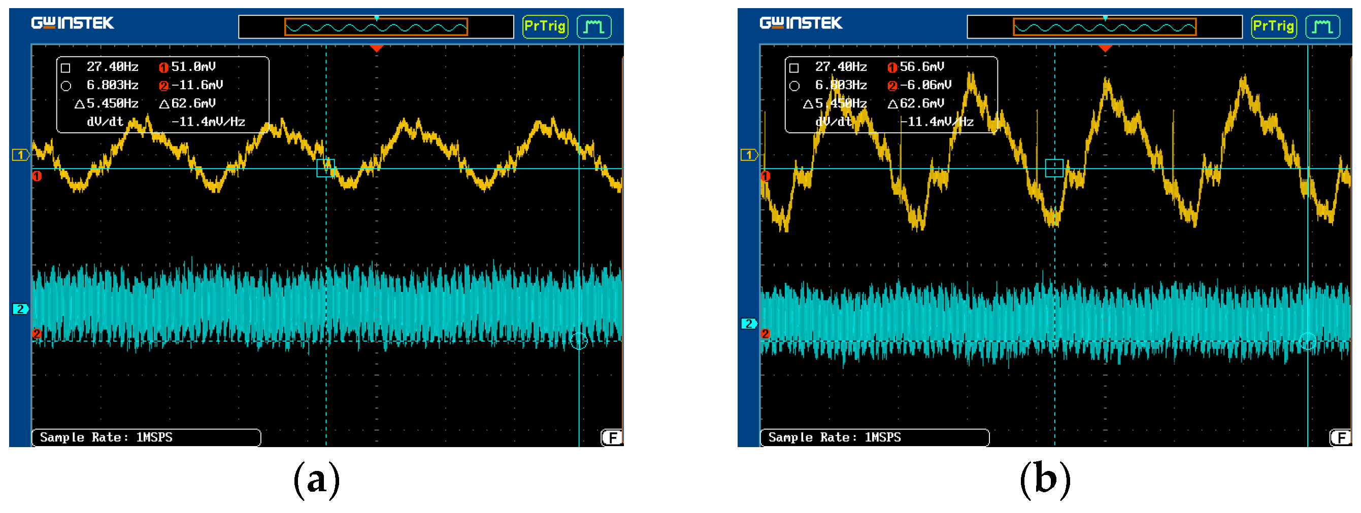
As illustrated in
Figure 6, a pronounced damage response of approximately 180 mV was clearly detected at the defect site. This distinct signal difference was observed by comparing the oscilloscope output under two probe conditions: perfectly aligned and misaligned with a lateral displacement of 10 mm. The significant voltage variation highlights the sensitivity of the measurement system to defect presence and positioning, demonstrating its capability for accurate defect localization and characterization in the tested material.
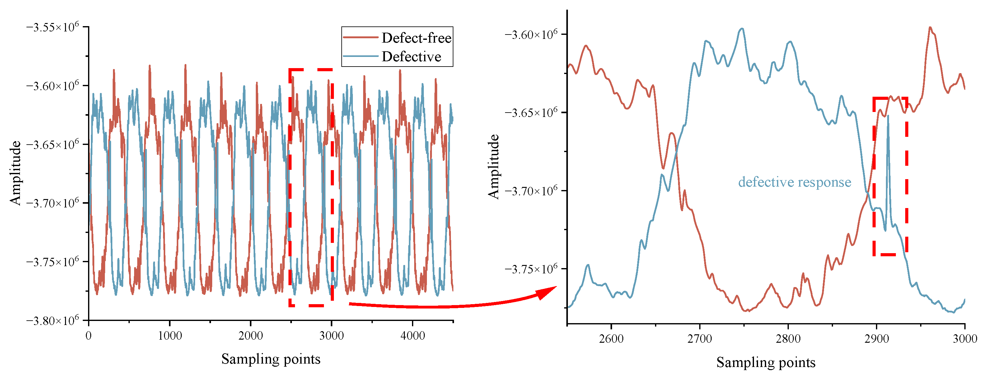
Figure 7 presents two sets of sample data received by the host computer over a one-second interval: the blue curve represents the data collected when aligned with the damage, exhibiting a distinct amplitude protrusion characteristic of the defect; the red curve corresponds to the misaligned state data, containing only noise with no other significant features.
4.1. The Low-Pass Filtering Residual Method
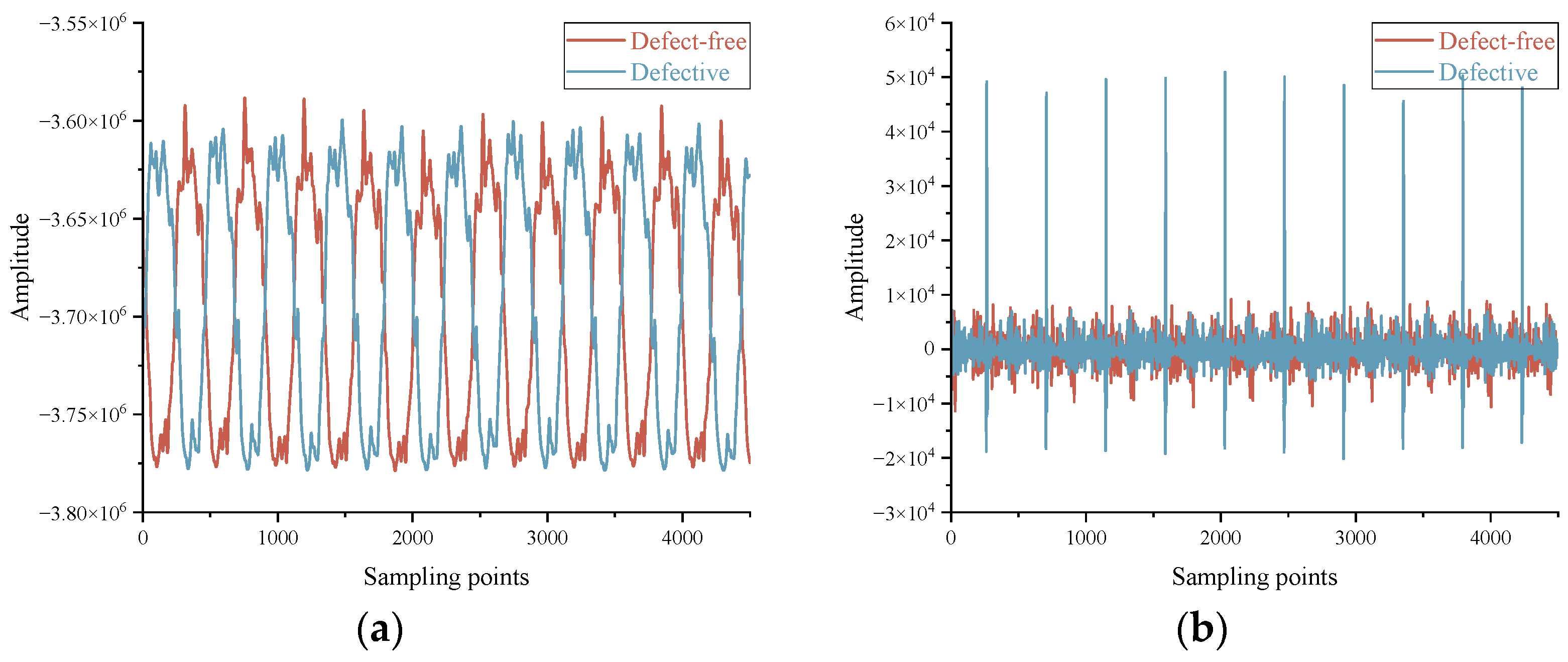
When processing signals in the time domain, a 12th-order FIR low-pass filter with a cutoff frequency of 100 Hz is first applied. After filtering, the defect response is largely suppressed (as shown in
Figure 8). The defect response is then precisely identified by calculating the residual between the original and filtered signals.
4.2. FT
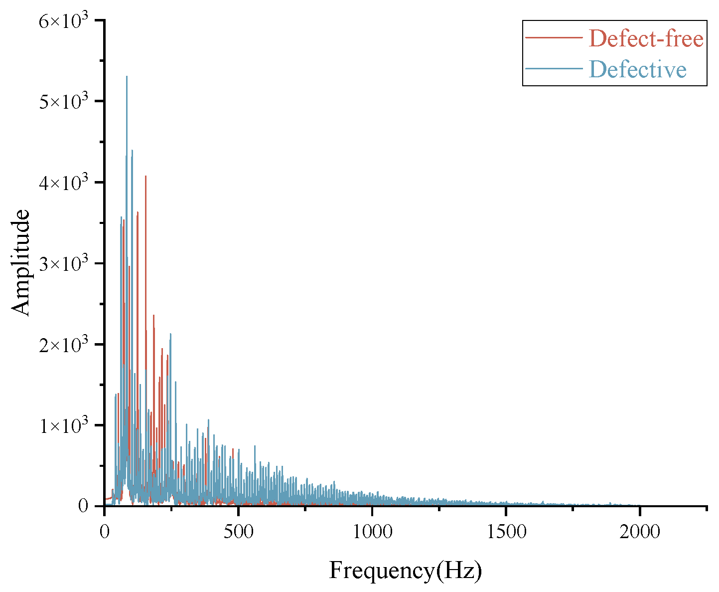
FT was applied separately to defect-free signals and defect-containing signals. A high-pass filter was first designed to extract high-frequency noise, followed by the Fourier Transform analysis of this noise (results shown in
Figure 9).
The results demonstrate that the Fourier Transform fails to accurately identify defect responses in the non-stationary signals output by the ECT system.
4.3. DWT
4.3.1. Single-Level Decomposition
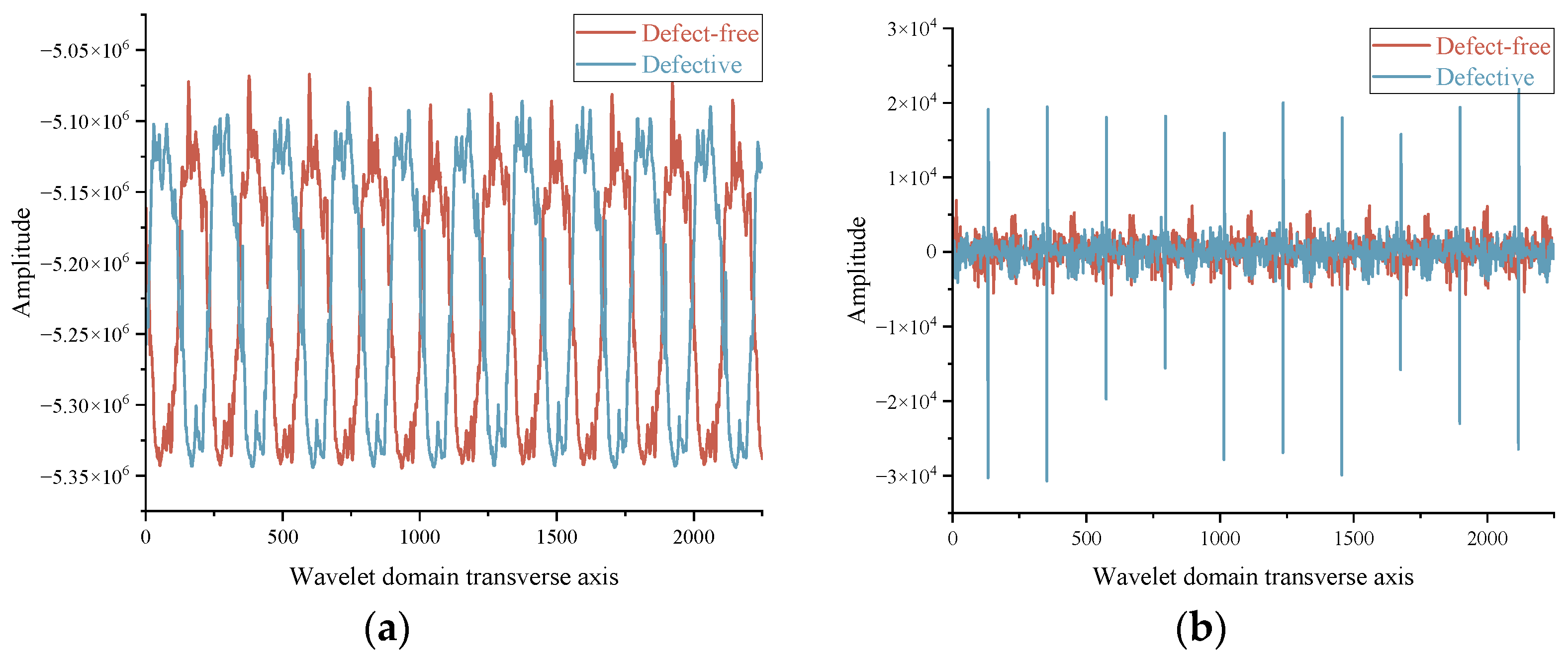
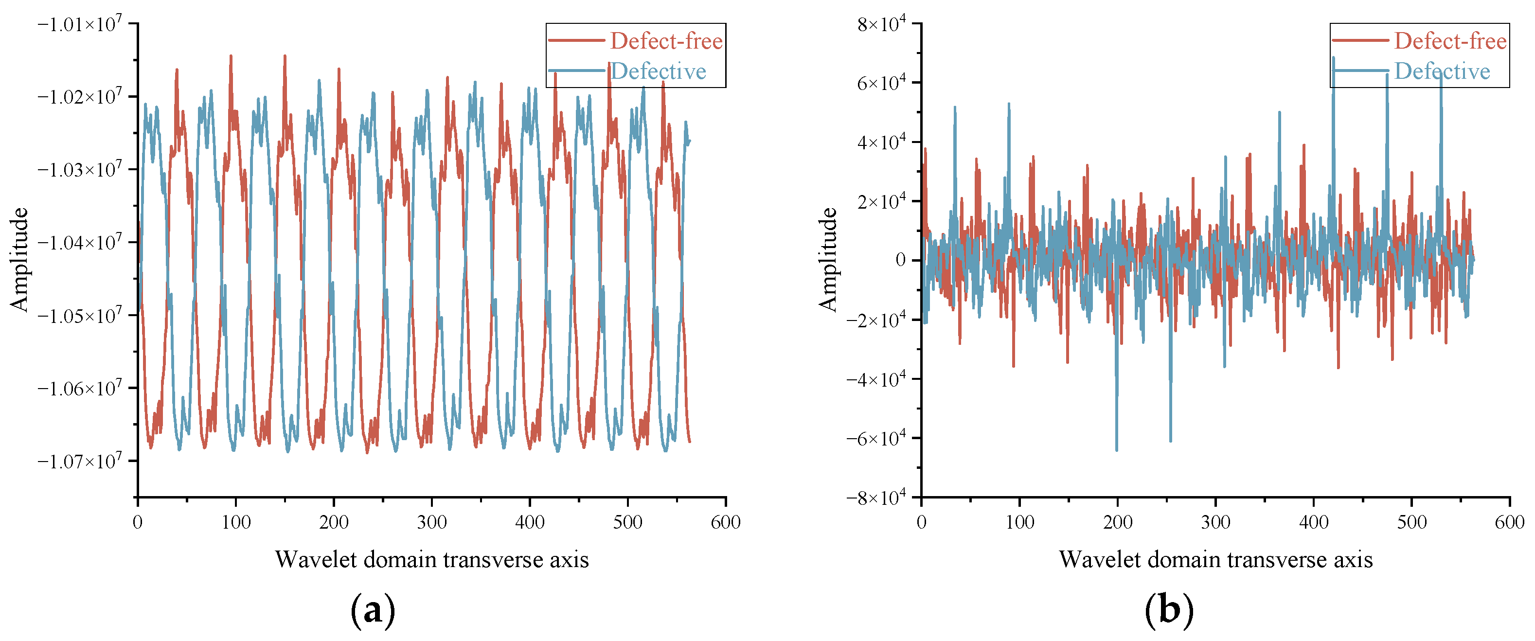
Figure 10 compares the single-level decomposition results of defect-free and defect-containing signals using the Haar wavelet: (a) approximation coefficients (
Figure 10a), and (b) detail coefficients (
Figure 10b). The horizontal axis represents the wavelet domain scale, carrying no direct physical interpretation. While the approximation coefficients (
a1) reflect the low-frequency characteristics of the signal, the detail coefficients (
d1) clearly reveal high-frequency defect responses.
4.3.2. Multilevel Decomposition
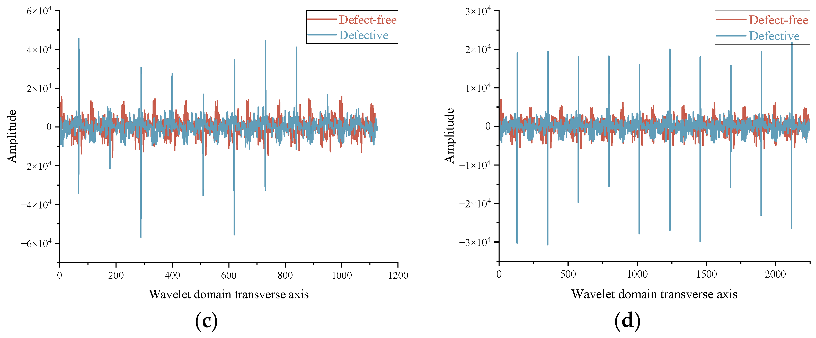
Figure 11 illustrates the three-level decomposition (
j = 3) of defect-free and defective signals using Haar wavelets, including the third-level approximation coefficients (a
3) and the first- to third-level detail coefficients (d
1–d
3). Results demonstrate that while the final-level approximation coefficients (a
3) characterize the low-frequency trend of the signal, only the first-level detail coefficients (d
1) effectively retain the defect response. Coefficients d
2 and d
3 fail to extract defect features effectively. Thus, a single-level DWT suffices for efficient extraction of defect characteristics.
4.4. Comparison of Results
Comparative analysis of the three signal processing algorithms reveals that FT fails to identify defect responses in non-stationary signals output by the ECT system. In contrast, the low-pass filtering residual method and the first-level DWT accurately detect defect responses. Specifically, the ΔSNR of the low-pass filtering residual method is 3.28 dB, while that of the first-level DWT reaches 3.64 dB—representing a 0.36 dB improvement over the former.
