Abstract
With advancements in remote sensing technology and very-large-scale integration (VLSI) circuit technology, the Earth observation capabilities of spaceborne synthetic aperture radar (SAR) have continuously improved, leading to significantly increased performance demands for on-board SAR real-time imaging processors. Currently, the low data access efficiency of traditional direct memory access (DMA) engines remains a critical technical bottleneck limiting the real-time processing performance of SAR imaging systems. To address this limitation, this paper proposes a dedicated instruction set for spaceborne SAR data transfer control, leveraging the memory access characteristics of DDR4 SDRAM and common data read/write address jump patterns during on-board SAR real-time imaging processing. This instruction set can significantly reduce the number of instructions required in DMA engine data access operations and optimize data access logic patterns. While effectively reducing memory resource usage, it also substantially enhances the data access efficiency of DMA engines. Based on the proposed dedicated instruction set, we designed a DMA engine optimized for efficient data access in on-board SAR real-time imaging processing scenarios. Module-level performance tests were conducted on this engine, and full-process imaging experiments were performed using an FPGA-based SAR imaging system. Experimental results demonstrate that, under spaceborne SAR imaging processing conditions, the proposed DMA engine achieves a receive data bandwidth of 2.385 GB/s and a transmit data bandwidth of 2.649 GB/s at a 200 MHz clock frequency, indicating excellent memory access bandwidth and efficiency. Furthermore, tests show that the complete SAR imaging system incorporating this DMA engine processes a 16 k × 16 k SAR image using the Chirp Scaling (CS) algorithm in 1.2325 s, representing a significant improvement in timeliness compared to existing solutions.
1. Introduction
Spaceborne synthetic aperture radar (SAR) is an active sensor based on the principle of microwave imaging. It obtains two-dimensional high-resolution images by transmitting broadband signals and applying synthetic aperture technology. Compared with traditional optical imaging and hyperspectral imaging, SAR imaging can eliminate the interference of clouds, fog, and nighttime, and features all-day, all-weather capability, high resolution, and a long detection range. Its application scenarios cover important national defense and civil fields such as Earth remote sensing, military reconnaissance, and resource exploration [1,2,3,4].
Since its development in the last century, spaceborne SAR has evolved from an initial single-view working mode to a satellite system with multiple functions, frequency bands, high resolution, operation modes, and polarizations. After the U.S. National Aeronautics and Space Administration (NASA) launched Seasat-A, the first synthetic aperture radar satellite in human history, in 1978, countries such as Germany, France, Japan, and Canada successively launched multiple SAR satellites. In 2016, China launched the Gaofen-3 satellite (GF-3), marking the beginning of China’s SAR remote sensing satellite era [3,5,6,7]. To date, dozens of spaceborne SAR systems are operational globally, and spaceborne SAR has become a critical means of Earth observation.
With the continuous development of spaceborne SAR, its imaging resolution, image size, and mapping swath have continuously improved, leading to exponential growth in the volume of data to be processed and the required processing speed. This has brought enormous pressure to spaceborne SAR data processing. Currently, the mainstream form of remote sensing data processing at home and abroad still relies on satellites acquiring data and then transferring it to ground systems for processing. This approach has a series of problems, such as excessive invalid data stored on the satellite, a low utilization rate of satellite payloads, a slightly long system response time, and a complex structure of ground reception and processing systems. Therefore, this form cannot meet actual needs such as the long-term continuous observation of ground target areas and rapid response to major events, making it difficult to achieve the widespread application and industrial development of remote sensing satellites. Based on the above issues, the remote sensing data processing form that completes SAR image processing in real time on board while the satellite acquires image data is more advantageous and of great research significance. The on-board real-time imaging processing of spaceborne SAR is the necessary means and development path for future SAR imaging processing [8].
However, although the on-board real-time imaging processing of spaceborne SAR has a series of development advantages, it also brings a series of challenges. The biggest challenge lies in the high real-time requirements of on-board SAR processing, which impose stricter demands on the processing speed of real-time processors [9,10,11,12,13].
For common SAR real-time imaging processors with pipeline architecture, their data processing speed is directly constrained by the bandwidth of the storage subsystem. Therefore, improving the bandwidth of the processor’s storage subsystem is of great significance for enhancing the processor’s imaging speed. In the processor’s storage subsystem, the DMA engine plays a critical role in data access and scheduling, serving as a key module in the storage subsystem [14,15,16]. After receiving transmission instructions from the CPU, the DMA directly accesses system memory and peripherals to complete data transfer between them without CPU intervention, acting as the sole bridge for high-speed transmission of large volumes of data between peripherals and memory in the processor. Therefore, the performance of the DMA engine directly determines the bandwidth of the storage subsystem [17,18].
For spaceborne SAR real-time processors, the processing of range and azimuth data in spaceborne SAR imaging algorithms leads to frequent address jump accesses by the DMA to the DDR memory in the real-time processor. After each address jump, data access requires redefining key parameters such as the data source address and target address of the DMA transmission, as well as configuring the DMA’s data transmission instructions and address change instructions. In the massive address jump data access operations of spaceborne SAR imaging, this significantly increases the instruction storage overhead, CPU occupation time by the DMA engine, and instruction execution time of the DMA engine. As a result, the DMA engine consumes excessive resources and has low data access efficiency, which is highly unfriendly to on-board processing scenarios with limited resources and high real-time requirements. Therefore, currently, the data access efficiency of the DMA engine has become a key bottleneck restricting the real-time performance of SAR on-board imaging processing. Optimizing the DMA data access strategy and hardware structure to improve data access efficiency has become one of the critical issues for enhancing the real-time performance of spaceborne SAR on-board processing [19,20,21,22].
At present, the ARM PL330W_DMA is widely used as a DMA engine in the field of on-board real-time imaging processing for spaceborne SAR. As a general-purpose DMA engine, it lacks specific descriptors for address-jumping data access and can only configure address-jumping instructions and data transfer instructions sequentially through the CPU. This leads to problems of excessive storage resource occupation and low data access efficiency. In addition to the ARM PL330W_DMA, researchers have proposed various optimized DMA architecture designs in recent years to improve data access efficiency in different application scenarios. For example, Sheng Ma, Yuanwu Lei et al. proposed a DMA in Reference [23] that supports efficient matrix transposition operations in digital signal processing. This DMA introduces a ping-pang multi-bank transposition buffer (MBTB), which can transpose multiple matrices per clock cycle and supports flexible transposition granularities of 32 bits, 64 bits, and 128 bits. However, it does not support out-of-order data arrival and pauses new requests until all elements of a matrix are transmitted, resulting in significant efficiency loss. Moreover, this DMA is only optimized for matrix transposition and does not address inefficiencies in other access-intensive tasks. Won Jun Lee and Chang Hyun Kim et al. proposed a dedicated processing-in-memory (PIM) instruction set for DMA in Reference [24]. It uses DMA descriptors to transfer PIM operation codes and operands, allowing a single descriptor to contain both PIM operation codes and operand information. This simplifies the programming model and improves instruction compilation efficiency, but the corresponding hardware architecture optimization for DMA is lacking, resulting in limited performance improvement and restricting its applicability across different systems. Davide Rossi et al. proposed an ultra-low-latency lightweight DMA engine for tightly coupled multi-core clusters in Reference [25]. By introducing a simplified microcode programming interface and lock-free command queues for each core, it significantly reduces programming complexity and efficiency losses caused by multi-core instruction execution arbitration. However, this DMA is specifically optimized for multi-core architectures, with minimal improvement in data access efficiency for single-core processors. Sheng Ma, Libo Huang et al. proposed a DMA engine for scientific computing accelerators in Reference [26]. It supports array reshaping transmission, parameter chaining mechanisms, and transmission chaining mechanisms, while integrating matrix transposition functions and optimizing matrix multiplication and DRAM access. However, its complex design and high hardware resource consumption make it unsuitable for resource-constrained on-board real-time processing scenarios.
From the above research, it can be seen that, in the field of on-board real-time imaging processing for spaceborne SAR, the problem of low data access efficiency caused by frequent address-jumping accesses of the DDR memory by the DMA engine in the processor remains unsolved. To address this, this paper proposes a DMA engine for the on-board real-time imaging processing of spaceborne SAR based on a dedicated instruction set, specifically optimizing the address-jumping data access strategy and hardware architecture of existing DMA engines. The main contributions of this paper are summarized as follows:
(1) By analyzing the algorithms of spaceborne SAR imaging, we summarized the common address-jumping data access patterns in on-board real-time imaging processing and proposed a dedicated instruction set for the DMA engine tailored to this scenario. This instruction set changes the access logic when the DMA engine accesses address-jumping data, reducing the instruction storage overhead and CPU occupation time during such accesses, thereby improving the instruction execution efficiency and data access speed of the DMA engine.
(2) Based on the innovative dedicated instruction set, we proposed a spaceborne SAR-specific state machine and designed a novel DMA engine hardware architecture. This architecture includes functional modules such as the ipu_r/w module for instruction fetching, decoding, and state machine control and the d1d_r/w module for AXI interface read/write operations. The entire DMA engine integrates one set of AXI_stream master interfaces, one set of AXI_stream slave interfaces, one set of AXI_full master interfaces, and one set of AXI_full slave interfaces.
(3) We performed logic synthesis, implementation, and module-level simulation tests on the proposed DMA engine, obtaining metrics such as logic resource usage, theoretical bandwidth, and data access efficiency. Additionally, we conducted imaging-level experimental tests. Using the VeriTiger-V19P experimental platform from HyperSilicon (Wuxi, China), we built a complete SAR imaging system incorporating the proposed DMA engine and tested the entire imaging workflow to verify the functionality and feasibility of the DMA engine. Experimental results show that the designed DMA engine achieves an average data read/write bandwidth of 2.517 GB/s (at 200 MHz) with an average data access efficiency of 84.46%. The imaging system using this DMA engine achieves an imaging time of 1.232 s, representing significant improvements over existing solutions.
The remainder of this paper is organized as follows: Section 2 analyzes DDR4 data access characteristics, summarizes common data access address patterns in the on-board real-time imaging processing of spaceborne SAR by combining typical spaceborne SAR algorithms, and outlines existing DMA engine data access strategies. Section 3 presents the content of the dedicated instruction set, analyzes its underlying working logic, and clarifies its significant advantages over existing general-purpose instruction sets. Section 4 proposes the design method for the dedicated state machine and introduces the overall hardware architecture and register definitions of the DMA engine. Section 5 describes the experimental setup and presents corresponding results. Finally, Section 6 concludes the paper and provides the main findings.
2. Problem
In this section, we first briefly introduce the classical CS algorithm workflow in the field of on-board imaging for spaceborne SAR, introduce the concepts of azimuth and range directions, and explain the fundamental reasons for the existence of address-jumping data access. Then, based on this, we outline the storage access characteristics of DDR4 SDRAM and summarize the common data address jump access patterns during the imaging process. Finally, we conduct a detailed analysis of how existing DMA engines handle data address jump accesses and clarify their application limitations in on-board real-time imaging processing for spaceborne SAR.
2.1. Analysis of the CS Algorithm
In the field of SAR imaging processing, the Chirp Scaling Algorithm (CS algorithm) is one of the most popular spaceborne SAR imaging algorithms. Compared with other imaging algorithms, the CS algorithm is characterized by high processing accuracy, strong noise resistance, and a fast imaging speed. Additionally, the CS algorithm mainly consists of operations such as Fast Fourier Transform (FFT), Inverse Fast Fourier Transform (IFFT), and complex multiplication, which can be implemented on hardware platforms like FPGAs and ASICs to provide high processing precision [27]. Therefore, the CS algorithm has become a popular choice for the on-board real-time imaging processing of spaceborne SAR.
The CS algorithm comprises three main processing steps, including operations on range-direction and azimuth-direction data of SAR echoes. The range direction refers to the direction in which the radar antenna transmits and receives signals, corresponding to the horizontal direction of image data, and represents the linear distance from the radar antenna to the target. The azimuth direction is perpendicular to the radar antenna’s pointing direction, corresponding to the vertical direction of the image, and represents the area covered by the radar platform during flight. The precise processing of data in both directions is the core of SAR imaging technology, jointly ensuring the resolution and quality of imaging results [1]. The specific steps of the algorithm are as follows:
Step 1: Chirp Scaling Processing: First, the Doppler center frequency (Fdc) is estimated. Then, FFT is used to transform the original two-dimensional time-domain data of SAR echoes from the azimuth direction to the range-Doppler domain. The data are then multiplied by the first phase function in the range-Doppler domain to complete the Chirp Scaling operation. This step ensures that the curvature of range migration curves is consistent across all range cells.
Step 2: Range Cell Migration Correction (RCMC), Range Compression, and Secondary Range Compression (SRC): After Step 1, the two-dimensional matrix in the range-Doppler domain is transformed into the two-dimensional frequency domain via FFT along the range direction. The data are then multiplied by the second phase function to complete RCMC and range compression. Subsequently, the data matrix in the two-dimensional frequency domain is transformed back to the range-Doppler domain by performing IFFT along the range direction.
Step 3: Azimuth Compression: First, the Doppler frequency rate (FDR) is estimated. Then, the two-dimensional matrix processed in Step 2 is multiplied by the third phase function in the azimuth direction within the range-Doppler domain to complete azimuth compression. Finally, IFFT is performed along the azimuth direction to transform the data from the range-Doppler domain to the two-dimensional time domain. After azimuth compression, the two-dimensional time-domain data are quantized to obtain the SAR imaging result.
The above are the three processing steps of the CS algorithm. Figure 1 shows a schematic diagram of the complete processing flow of the CS algorithm.
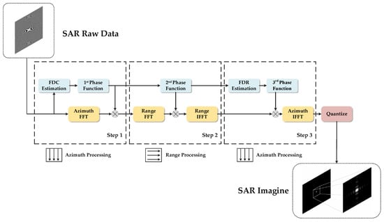
Figure 1.
The schematic flowchart of CS algorithm processing.
From the algorithm steps and schematic diagram of CS, it can be seen that the algorithm processing requires continuous switching between the azimuth and range directions for data access and processing. Since the data in the two directions correspond to the horizontal and vertical directions of the image data, and their storage positions in DDR are perpendicular to each other, each switch of the data access direction may point to address regions far apart in the memory, i.e., non-continuous address regions. Therefore, frequent address jump access occurs in the hardware implementation of the CS algorithm process, which has become one of the key factors affecting the execution efficiency of the CS algorithm in hardware implementation.
2.2. Analysis of Storage Access Characteristics
2.2.1. Introduction to DDR4 SDRAM
During the SAR imaging processing, a large amount of raw echo data and intermediate processing data need to be stored. DDR4 SDRAM is currently the ideal off-chip storage medium for the real-time processing of spaceborne SAR. As a storage chip, DDR4 SDRAM can be regarded as a matrix storage sequence composed of banks, rows, and columns. Each bank consists of many rows and columns, and the position determined by the intersection of each row and column is called a storage cell. The schematic diagram and physical image of DDR4 SDRAM are shown in Figure 2 [28].
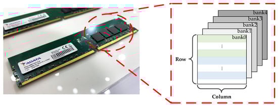
Figure 2.
The schematic diagram and physical image of DDR4 SDRAM.
DDR4 SDRAM typically has 8 or 16 banks, each containing thousands of rows and columns. To locate a storage cell, the DDR4 addressing process first specifies the bank address, followed by the row address, and finally the column address. Read and write access to DDR4 is achieved through the burst transmission of consecutive storage cells in the same row. The burst length is the number of consecutive transmission cycles. In this burst transmission mode, once the start address and burst length are specified, the memory automatically reads or writes data to the corresponding number of storage cells in sequence without requiring the controller to continuously provide addresses [29,30,31]. The burst length of DDR4 can be configured as 4 or 8 as needed. In most cases, to achieve higher DDR4 access bandwidth, the burst length is typically set to 8, meaning the memory consecutively reads from or writes to 8 address data on the rising and falling edges of four clock cycles.
In DDR4 SDRAM, raw SAR echo data are stored in a matrix format, where the range direction corresponds to rows in DDR4 and the azimuth direction corresponds to columns. The storage mapping process is shown in Figure 3 [32].
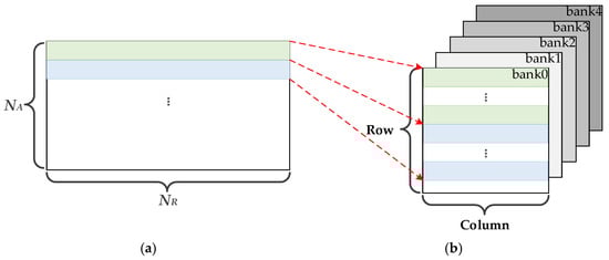
Figure 3.
(a) Schematic diagram of SAR image. (b) Schematic diagram of SAR image mapping to storage in DDR.
2.2.2. Analysis of Data Read/Write Address Change Patterns
In this subsection, we analyze two classic scenarios of address-jumping data access in the process of spaceborne SAR imaging processing.
First, taking the data read/write patterns of the DMA engine during transposition as an example, we analyze the address-jumping data access scenarios that occur in the on-board imaging process of spaceborne SAR. Transposition is a unique and crucial operation in the storage subsystem of spaceborne SAR imaging. From the analysis of the CS algorithm workflow, it is known that, during the real-time imaging processing of spaceborne SAR, azimuth-direction data and range-direction data need to be processed separately, corresponding to rows and columns in DDR4, respectively. Moreover, due to the row-burst read/write mechanism of the memory, there is generally a significant difference in the data read/write rates between rows and columns. To balance this speed gap and ensure matching computation rates in the azimuth and range directions, thereby improving the operational efficiency of SAR imaging algorithms, the data transposition method emerged, and it plays an important role in the on-board real-time imaging processing of spaceborne SAR, serving as one of the essential steps.
The “three-dimensional cross-mapping transposition method based on matrix partitioning” is one of the classic transposition methods in the field of SAR imaging processing. In this section, we first take the classic application scenario of using this method for transposition as an example to analyze the address change patterns of the DMA engine when reading and writing SAR data during the transposition process. According to the specific content of the transposition method, a complete image dataset of NR × NA × 64 bits can be divided into several 256 × 256 submatrix blocks, as shown in Figure 4, where NR corresponds to azimuth-direction data and NA corresponds to range-direction data.
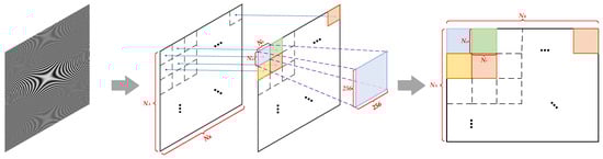
Figure 4.
Schematic diagram of image data transposition and division.
During the transposition process, the DMA engine is required to read data from each submatrix block sequentially, send it to a dedicated transposition module, and, after transposition, write the output data back to the original storage locations of the corresponding submatrix blocks using the DMA engine again. The engine reads the submatrices from left to right and top to bottom. Within each submatrix, data are also read in sequence from left to right and top to bottom [33].
The specific data reading process is as follows:
First, the first submatrix block is read. Data within the submatrix are read row by row in the burst mode. After reading 256 data points from each row, the access address jumps to the starting position of the next row to continue reading from left to right until all 256 data points in the 256th row are read, thus completing the reading of the first submatrix block. Subsequently, the access address jumps to the starting position of the next submatrix block. A schematic diagram of this process is shown in Figure 5, where the solid black arrows represent the data read/write process, and the dashed red arrows represent the address jump process during data access.
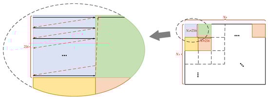
Figure 5.
Data reading process of submatrix blocks.
After completing the data reading of the first submatrix block, the second, third, fourth, and subsequent submatrix blocks in the same row are read sequentially to the right in the same manner until all submatrix blocks in the first row are processed. Subsequently, the access address jumps to the starting position of the first submatrix block in the next row. A schematic diagram of this process is shown in Figure 6.
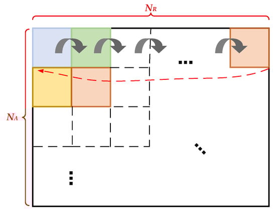
Figure 6.
Process of reading a row of submatrix blocks.
After completing the data reading of all submatrix blocks in the first row, the same process is repeated for the second, third, fourth, and subsequent rows, moving downward sequentially until the last row. This ensures that all submatrix blocks in the entire image are traversed and read. A schematic diagram of this process is shown in Figure 7.
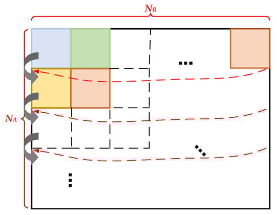
Figure 7.
Process of reading submatrix blocks in all columns.
After the transposition module completes data transposition, the DMA engine sequentially writes the module’s output data back to the original storage locations of the corresponding submatrix blocks. The specific data write address change pattern is completely consistent with that during data reading.
In addition, the cropping operation is also a critical task in spaceborne SAR imaging processing. It can remove edge parts and non-interest areas in the image, focus attention on specific target regions, reduce the amount of data requiring processing and storage, improve the processing efficiency of spaceborne SAR imaging, and lower storage costs.
The specific operation process of cropping is as follows:
Data reading starts from an arbitrary position in a row of the complete image. After reading a certain length, the access address jumps to the same starting position in the next row and reads the same data length until the required area is fully read. A schematic diagram of this process is shown in Figure 8, where solid black arrows represent the data read/write process, and dashed red arrows represent the address jump process during data access [34,35].
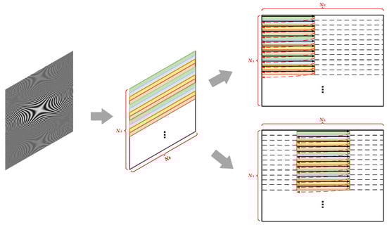
Figure 8.
Schematic diagram of image local truncation operation.
In addition to the two operations mentioned above, imaging processing also involves a series of operations such as zero padding and stitching, which share similar data read/write access patterns. Through the analysis of these typical data access operations in spaceborne SAR imaging processing, it can be concluded that, during imaging, there are numerous data read/write scenarios with discontinuous access addresses but fixed and repetitive address jump patterns. Compared to random address jump access, fixed and repetitive address jump patterns are easier to describe using loop statements rather than enumerating all address jumps one by one. This provides critical theoretical support for designing a spaceborne SAR real-time processing DMA engine based on a dedicated instruction set [36].
2.3. Analysis of Functionalities of Existing DMA Engines
In the storage subsystem of a spaceborne SAR real-time imaging processor, the DMA engine plays a crucial role in data access and scheduling, serving as an indispensable key module. It enables communication between hardware devices operating at different speeds without relying heavily on the central processing unit (CPU) for interrupt handling. During DMA operation, the CPU first sends a transfer request and DMA commands containing configuration information to the DMA. The DMA then performs data transfer based on parameters specified in the commands, such as source address, destination address, transfer length, burst length, and burst size. Upon completion, the DMA issues an interrupt to notify the CPU that the transfer has ended, allowing the relevant tasks to be closed.
Currently, the ARM PL330W_DMA is widely used in spaceborne SAR real-time imaging processors. Designed by ARM specifically for embedded systems, its versatile architecture makes it suitable for various applications, including multimedia processing, network communication, and SAR imaging. As a critical component for high-performance data transfer [37], its hardware structure is illustrated in Figure 9.
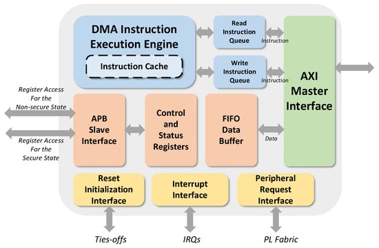
Figure 9.
Schematic diagram of ARM PL330W DMA engine structure.
As a general-purpose DMA engine, it provides a set of universal data transfer instruction sets, as shown in Table 1.

Table 1.
General instruction set used by ARM PL330W DMA.
From the functions of each instruction in the instruction set, it can be seen that the PL330_DMA can flexibly access data from any source address and transfer it to any destination address. However, it cannot automatically perform address-jumping data access under the control of a single instruction. For instance, each instruction can only control the DMA engine to access and transfer a segment of consecutive address data. When accessing the next segment of non-consecutive addresses, a new transfer instruction needs to be reconfigured [37].
For example, when using the general instruction set provided by the PL330W_DMA to describe the specific process of the transposition operation listed in Section 2.2.2, a combination of a DMARMB instruction and a DMAST instruction is required for each transfer of 256 consecutive data points in a row. The specific process can be summarized into the following pseudocode, as shown in Table 2:
Table 2.
Pseudocode describing the transposition operation using the general instruction set.
From the pseudocode, it can be observed that, during the transposition operation, excluding initialization-related instruction statements such as configuring registers and setting up interrupts, and considering only the number of data read/write instruction statements and starting address setting instruction statements, the number of instructions required when using the general instruction set is calculated as follows:
256 × (Nr/256) × (Na/256) × 2
For a typical SAR image of size 64 k × 16 k (i.e., Na = 64 k, Nr = 16 k), approximately 8,000,000 instruction statements are required, which is quite substantial. The use of excessive instruction statements has a series of significant drawbacks. First, the on-board imaging processing environment has limited resources, and an excessive number of instructions occupy a large amount of storage space. For a 64-bit ARM core, the storage size occupied by each instruction is approximately 8 bytes. Based on the above calculation of the number of instructions required by the PL330W_DMA, the required storage space is roughly calculated as follows:
256 × (Nr/256) × (Na/256) × 2 × 8 byte
For a SAR image of size 64 k × 16 k (i.e., Na = 64 k, Nr = 16 k), the required storage space is 64 MB. This occupies more of the effective storage space of the spaceborne SAR processor. In addition, an excessive number of instructions will take up more operating time of the CPU, affecting the performance of the CPU and even the entire processor. For the DMA engine, each instruction requires to be configured by the CPU. For a 64-bit ARM core, each instruction takes 20 to 30 clock cycles. Considering that the pl330w_DMA requires one DMARMB instruction and one DMAST instruction to transfer consecutive address data each time, approximately 50 clock cycles of the CPU are occupied. When the CPU frequency is 400 MHz, this takes about 1 s of CPU time. This will significantly reduce the CPU’s ability to handle other tasks, increase the delay of other interrupt transactions, reduce processing efficiency, and seriously affect the performance of the processor. Moreover, for the pl330w_DMA using a general instruction set, each transfer of consecutive address data requires waiting for the CPU to configure instructions and for the engine to compile the instructions. In the application scenario of spaceborne SAR imaging processing with a large number of address jump data accesses, this mode will cause the data transfer speed of the DMA engine to be restricted by the CPU’s operating speed, seriously limiting the performance of the DMA engine.
In the process of on-board real-time imaging processing for spaceborne SAR, there are numerous scenarios involving fixed repetitive address-jumping data access represented by transposed data reading and writing, which can be easily described using loop languages. According to the above analysis, for the pl330w_DMA, in such application scenarios, it is necessary to repeatedly configure and execute hundreds or thousands of data transmission commands and address increment commands. This not only increases the storage resource overhead of instructions but also prolongs the CPU occupation time and the instruction execution duration of the DMA engine, ultimately reducing the efficiency of DMA data access. Therefore, although the pl330w_DMA is flexible and has good performance, it is not suitable for the on-board real-time imaging processing application scenarios of spaceborne SAR with high real-time requirements and limited on-board storage resources. Against this background, designing a spaceborne SAR real-time processing DMA engine based on a dedicated instruction set, using the dedicated instruction set to simply describe fixed repetitive address-jumping data transmission behaviors, and optimizing the instruction execution strategy are of great significance.
3. Design of Special Instruction Set for DMA Engine in Spaceborne SAR Data Transmission Control
3.1. Content of the Instruction Set
As analyzed in Section 2, during the on-board real-time imaging processing of spaceborne SAR, there are numerous data access scenarios similar to transposed data reading and writing, all of which feature fixed and repetitive address-jumping patterns. Specifically, this means that the read/write length of consecutive address data is consistent each time, the address increment for each data access address jump is uniform, and the same data read/write operations and address jump operations are repeated hundreds or thousands of times. Therefore, compared with the general logical thinking of describing data access one by one in a general-purpose instruction set, using logical loop statements to describe the above data access behaviors is more appropriate. Logical loop statements can repeatedly execute fixed data read/write and address increment operations thousands of times without additionally increasing instruction statements, which is highly compatible with the data access characteristics in the on-board real-time imaging processing of spaceborne SAR.
Based on the above design philosophy, this paper proposes a set of special instruction sets for spaceborne SAR data transmission control, which uses six instructions to support flexible multi-nested data address jump reading and writing. The specific contents of the special instruction set are as follows:
- 1.
- INS_DMAEND:
The instruction label being 0 indicates the end of the DMA command. Except for the high 8 bits, other bits do not need to be configured, as shown in Figure 10.

Figure 10.
INS_DMAEND instruction.
- 2.
- INS_SETADD:
Instruction label: 1. When bit 55 is 0, this instruction sets the starting value of the source address; when bit 55 is 1, it sets the starting value of the destination address. The address bit width is 35 bits. The specific configuration method is shown in Figure 11.
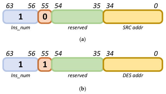
Figure 11.
INS_SETADD instruction. (a) Setting the starting value of the source address. (b) Setting the starting value of the destination address.
- 3.
- INS_ADDADDR:
The instruction label is 2. When the 55th bit is 0, this instruction sets the source address jump increment; when the 55th bit is 1, it sets the destination address jump increment. The address width is 35 bits, and the specific configuration method is shown in Figure 12. It should be noted that the two’s complement of the address must be used for address subtraction.
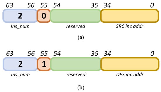
Figure 12.
INS_ADDADDR instruction. (a) Setting the source address jump increment. (b) Setting the destination address jump increment.
- 4.
- INS_LOOP:
The instruction label is 3, indicating a loop. The loop count has a bit width of 20 bits. Refer to Figure 13 for the configuration method.
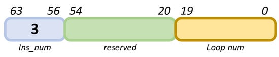
Figure 13.
INS_LOOP instruction.
- 5.
- INS_LOOPEND:
The instruction label is 4, indicating the end of a loop. The remaining bits do not need to be configured, as shown in Figure 14.

Figure 14.
INS_LOOPEND instruction.
- 6.
- INS_D1D:
The instruction label is 5, representing a one-dimensional DMA read/write instruction. When the 55th bit is 0, this instruction is a read command; when the 55th bit is 1, it is a write command. The specific configuration method is shown in Figure 15.
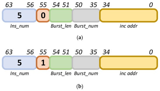
Figure 15.
INS_D1D instruction. (a) Read command, Perform read operation; (b) Write command, Perform write operation.
The above dedicated instruction set summarizes the access characteristics of data read/write operations in on-board SAR imaging processing, revolutionizing the traditional address-hopping data access logic. Through combinations of these instructions, it is possible to describe any regularly repeating address-hopping data access patterns in imaging processing with a compact set of instructions, making it highly suitable for classic application scenarios in on-board SAR imaging processing.
3.2. Analysis of Instruction Set Application
Taking the transposed data read/write listed in Section 2.2.2 as an example, the dedicated instruction set is used to describe the address-hopping data access in the operation process, and its effects are analyzed.
During the transposition process, the role of the DMA engine is to read SAR image data with a size of NR × NA × 64 bit stored in DDR4 SDRAM in blocks, send it to the transposition module, and then read the transposed data from the transposition module and send it to DDR4 SDRAM. According to the analysis in Section 2.2.2, the complete process of the DMA engine reading data is shown in Figure 16, and the data writing process is consistent with it. As can be seen from the schematic diagram, the entire data reading process involves three layers of loop nesting.
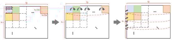
Figure 16.
Schematic diagram of the complete transposition operation process.
The process described above can be represented using the dedicated instruction set proposed in this paper, resulting in the pseudocode shown in Table 3.
Table 3.
Pseudocode described by the special instruction set for transposition operation.
The specific process is described as follows:
First, the DMA transfer is initiated using the DMASTART instruction, and the transfer-related parameters for the DMA registers are configured through the APB interface.
Then, the D1D_R instruction is used to sequentially read the 256 data items in the first row of the first submatrix block; after the read is completed, the ADDADDR instruction is used to increase the data access address by (Nr-256), causing the data access address to jump to the starting position of the second row of data in the submatrix block; then, the LOOP command is used to repeat the above reading and address jumping operations 256 times, completing the traversal read and write of the data in the first submatrix block; finally, the loopend command is used to end the first layer of loop, that is, the innermost loop.
After the first layer of loop is completed, the ADDADDR command is used to increase the address by (Nr-256), causing the data access address to jump to the starting position of the first row of data in the second submatrix block; then, the LOOP command is used to repeat the above inner loop and address increase operations Nr/256 times, completing the traversal read and write of the data in the first row of submatrix blocks; finally, the loopend command is used to end the second layer of loop.
After the second layer of loop is completed, the ADDADDR command is used to increase the address by (-Nr × 256), causing the data access address to jump to the upper left corner of the first submatrix block in the second row; then, the LOOP command is used to repeat the above second layer of loop and address increase operations Na/256 times, completing the traversal read and write of the data in all submatrix blocks of the entire image; finally, the loopend command is used to end the third layer of loop, that is, the outermost loop.
After the three-layer loop reading is completed, the DMAEND command is used to end the DMA transfer task.
The way the DMA engine writes the transposed data back to the DDR is similar to the above reading method. Simply replacing the D1D_R instruction in the pseudocode with the D1D_W instruction will achieve this.
From the pseudocode above, it is evident that, when performing transposition operations, the dedicated instruction set offers remarkable conciseness in describing the complete data read/write process. Excluding initialization instructions (e.g., configuring registers, setting up interrupts), and focusing solely on data read/write and address-setting instructions, the dedicated instruction set requires only a dozen DMA instructions regardless of the SAR image size. This contrasts sharply with the general instruction set used by PL330W_DMA, which generates millions of instructions for the same task. The storage space occupied by the dedicated instruction set is negligible in comparison.
Additionally, on a 64-bit ARM core, each instruction consumes 20–30 clock cycles. Thus, the dozen DMA instructions of the dedicated instruction set only require 200–300 CPU clock cycles—minimal overhead that does not impact CPU processing capabilities.
Compared to the PL330W_DMA, which relies on the CPU to configure instructions and whose data transfer speed is constrained by CPU performance, the XDMA engine with a dedicated instruction set achieves an extremely low ratio of instruction count to transferred data volume. This means that each DMA instruction configures the engine to transfer a large amount of data without frequent CPU intervention during the transfer process. This resolves the bottleneck introduced by the general instruction set, liberates DMA data transfer from CPU speed constraints, and maximizes engine performance. In addition to the above advantages, the significant reduction in the number of operation instructions also effectively reduces the power consumption during the operation of the DMA engine. Taking the transpose operation as an example, based on the post-silicon test results of previous chips and statistical analysis (by testing the power consumption of a single DMA engine behavior of the test chip and counting the corresponding number of instructions used, the power consumption per instruction at the corresponding frequency can be roughly calculated), the dedicated instruction set can enable the DMA engine to save more than 10 w of power consumption (at 300 MHz) during each transpose operation, which is of great advantage in the satellite environment with strict power consumption constraints.
In other scenarios of on-board real-time SAR imaging processing, data access patterns similar to transposition operations—characterized by discontinuous addresses with fixed, repetitive jump patterns—are common. A detailed analysis of various data read and write scenarios reveals that they are all composed of fundamentally identical basic operations arranged and combined in different ways, with transposed data access being one of the most complex cases. Therefore, the analysis above can be extrapolated to these scenarios. A comparison of instruction counts across scenarios is presented in Table 4.
Table 4.
Comparison of the number of instructions used in other on-board imaging scenarios.
It can be concluded that, compared with traditional general-purpose DMA instruction sets, the dedicated instruction set proposed in this paper significantly reduces the number of instructions required for address-jumping data access in spaceborne SAR imaging scenarios involving extensive address transitions. This reduction saves substantial instruction storage overhead, effectively shortens CPU occupation time, and greatly improves the data transfer rate of the DMA engine, fully unleashing the engine’s performance potential. The dedicated instruction set thus holds broad application prospects in the field of SAR imaging.
4. Hardware Design of the DMA Engine
Building upon the dedicated instruction set proposed in Section 3, this section presents a hardware architecture for a spaceborne SAR real-time processing DMA engine based on the dedicated instruction set. During on-board real-time SAR imaging, this DMA engine enables efficient access to data with repetitive address jumps using concise control instructions and optimized state machine transition logic. This design reduces storage overhead, alleviates CPU workload, and enhances data transfer rates, meeting the requirements of low resource consumption and high transfer efficiency in on-board SAR imaging. The overall structure of the DMA engine is illustrated in Figure 17.
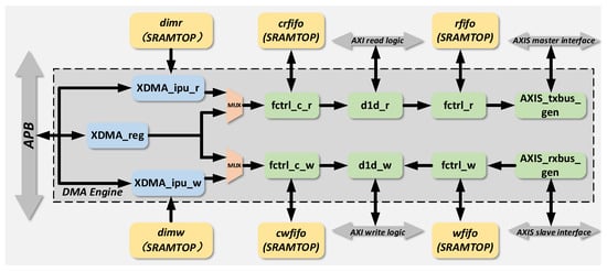
Figure 17.
Hardware structure diagram of imaging-specific DMA engine.
As illustrated in the hardware architecture diagram, the engine is primarily composed of modules such as xdma_ipu_r/w, xdma_reg, and d1d_r/w. Among them, xdma_ipu_r/w is responsible for reading and parsing DMA instructions, as well as controlling state machine jumps; xdma_reg handles register configuration; and d1d_r/w serves as the AXI interface logic. Specific descriptions of each module are provided in the following subsections.
The specific workflow of the engine is as follows: First, the APB bus configures the transfer-related registers in xdma_reg. After the register configuration is completed, data access operation instructions are written into dimr/w through the APB bus (for the CPU of the chip, it is equivalent to the conventional behavior of writing data to a specific memory address via the APB bus, without the need to add new drivers or compilers). Subsequently, the ipu module reads the instructions and parses them internally, controlling the internal state machine jumps based on the parsed instructions. After the state machine jumps, control signals are outputted, entering d1d_r/w through the fctrl_c_r/w module to control the d1d_r/w module to perform data read/write operations.
This DMA engine supports three data transmission modes during operation: The AXI read interface in d1d_r reads data from the bus and outputs the data to other addresses on the bus through the AXIS_master interface, i.e., AXI in and AXIS out. The AXIS_slave receives data from the bus and outputs the data to other addresses on the bus through the AXI write interface in d1d_w, i.e., AXIS in and AXI out. Directly interconnecting the AXIS_master interface and the AXIS_slave interface outside the DMA engine can implement a data transmission path from the AXI read interface to the AXIS_master interface to the AXIS_slave interface to the AXI write interface, i.e., AXI in and AXI out.
The above three transmission modes can cover most application scenarios of on-board real-time imaging processing for spaceborne SAR.
4.1. Design of State Machine Based on Dedicated Instruction Set
The state machine is the core for implementing the dedicated instruction set functions of the DMA engine in the real-time processing of spaceborne SAR. Compared with the numerous states and complex state transition logic of the ARM pl330w_DMA [37], this paper proposes a dedicated state machine for spaceborne SAR data transmission by combining the application requirements of the on-board real-time imaging processing of spaceborne SAR and the design of a dedicated instruction set for spaceborne SAR data transmission control. The specific design ideas are as follows: streamline the number of states in the state machine, retaining only those relevant to the spaceborne SAR imaging scenario; simplify the transition logic between states to ensure a one-to-one correspondence between transition triggers and instruction set content; and reduce the number of secondary states corresponding to each state and add a “loop” state for spaceborne SAR imaging applications. The state transition diagram of the state machine is shown in Figure 18.
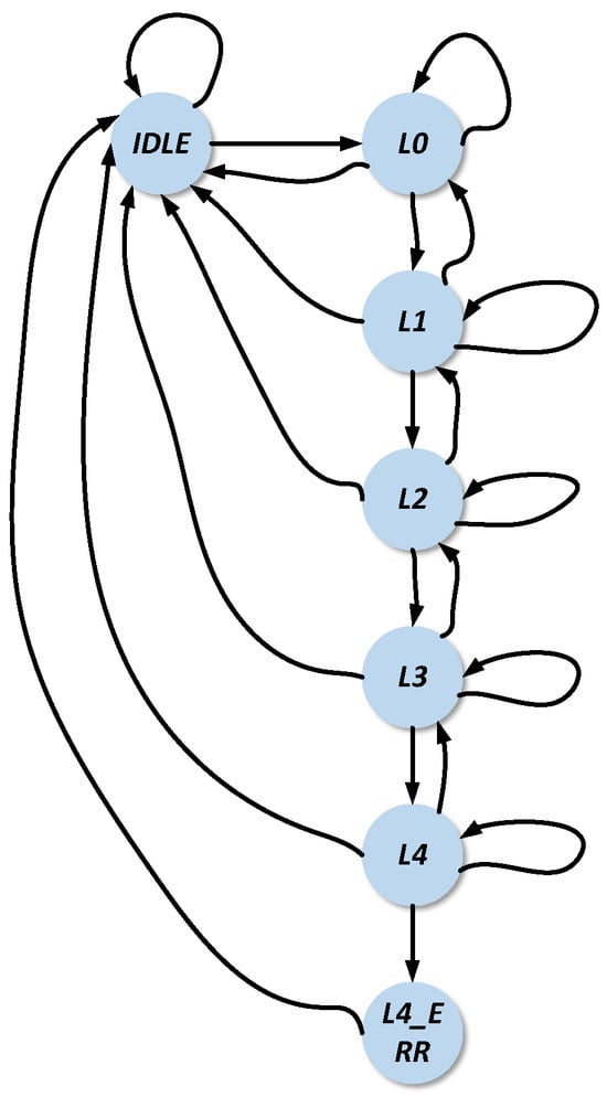
Figure 18.
Design of specialized state machine based on specialized instruction set.
The states and transition conditions of the state machine are described as follows:
IDLE: The DMA engine is in an idle state, which serves as the initial state with no operations being performed. Upon the receipt of the DMA_START pulse signal by the DMA controller, the CPU activates the DMA controller to initiate operations, triggering a transition to state L0.
L0: This state is entered upon the activation of the state machine. When an instruction parsed as LOOP is received, the state machine transitions to L1 to initiate the first-level loop operation. If the instruction DMAEND is received, the state machine reverts to IDLE, entering the idle state. In the absence of any instruction, the state remains at L0 with no transition.
L1/2/3: These states correspond to the first, second, and third levels of software loops, respectively. During loop operations, the state machine controls cyclic data access based on pre-configured transmission parameters. Transition to L2/3/4 occurs when a LOOP instruction is parsed. Receipt of DMAEND triggers a transition to IDLE. If a LOOP instruction is received and loop counters for levels 1–3 reach zero, the state machine returns to L1/2/3; otherwise, it remains in the current state.
L4: This state represents the outermost software loop. Considering the practical requirements of on-board real-time imaging for spaceborne SAR and balancing resource utilization with application needs, the state machine is designed with a maximum of four loop levels. If loop configurations exceed four levels, the state machine transitions to L4_ERR.
L4_ERR: This state indicates an error condition. Since the maximum supported loop level is four, any attempt to execute more than four nested loops during runtime causes the state machine to enter L4_ERR, followed by a transition to IDLE in the next clock cycle.
From the overall description of the state machine and the detailed explanation of each state, it can be seen that the state machine has simple transition logic, few state branches, and low complexity. Moreover, each state has the ability to return to the IDLE state in the event of an anomaly, which greatly ensures robustness in the complex working environment on a satellite. Compared with the traditional DMA scheme that features a general, redundant, and complex state machine design, this approach significantly enhances the reliability of operation.
In addition, as can be seen from the structure of the state machine, its essence lies in the logical mapping of software for-loop statements. This design features a concise logical structure, ensuring high readability and maintainability. Each state within the dedicated state machine fully addresses the requirements of various application scenarios in the on-board real-time imaging processing of spaceborne SAR. Redundant states from the generic instruction set of ARM pl330w_DMA, such as “At Barrier”, “Updating PC”, and “Waiting for Peripheral”, which are irrelevant to spaceborne SAR applications, have been systematically removed. This streamlining effectively reduces the number of decision points between state transitions, simplifies decision-making logic, and thereby shortens decision latency and enhances state transition efficiency.
Moreover, the simplified state machine significantly reduces conditional branching logic, minimizing the likelihood of CPU branch prediction failures and shortening the execution time of branch instructions. The direct one-to-one correspondence between state transition conditions and the dedicated instruction set described earlier improves system predictability, streamlines development and maintenance processes, and enhances system security and flexibility by reducing errors and unexpected behaviors. This alignment also facilitates future system expansions and automated testing, enabling the state machine to readily adapt to evolving application requirements.
4.2. Xdma_ipu Read/Write Module
This module serves as the core functional unit of the DMA engine and primarily incorporates three logical components: instruction fetch logic, instruction decoding logic, and the state machine with associated control logic. The design philosophy of this module is to hierarchically integrate these three logical components into a single module to ensure efficient interaction between them. It explicitly defines the input as instruction control signals from the DMA engine and the output as state machine transition commands, ensuring that the mapping from instructions to state transitions is handled autonomously within the module. Additionally, dedicated interfaces are designed for different functions: the APB interface manages register access and configuration data reception, the AXI interface transmits state machine status to the data access module, and the MEM interface accesses instructions stored in SRAMTOP. This interface design ensures independent and efficient data exchange with other functional modules while preventing interference. The structural diagram of the module is shown in Figure 19.
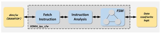
Figure 19.
Schematic diagram of XDMA_IPU read/write module structure.
When the module receives the xdma_start pulse signal configured in the register, it initiates the first read operation from the DIM (DMA Instruction Memory) to access the instructions stored therein. During subsequent operations, the DIMR/W (DMA Instruction Memory Read/Write) is accessed again under the following conditions: when the parsed instruction is setaddr, addaddr, loop, or loopend and the instruction is valid; when the instruction is parsed as d1d, the module checks the register to confirm whether the next-level receive/transmit FIFO is full/empty. If the instruction is parsed as loopend and the current loop counter has not reached zero, the module jumps back to the memory location of the current loop to re-read the instructions for cyclic operations; otherwise, it continues to sequentially read the instructions following loopend in the DIM. When the instruction is parsed as dmaend, the XDMA instruction operations terminate.
Upon reading an instruction, the module executes decoding logic to parse six types of instructions, along with associated parameters such as address jump values and loop counts. The decoded instructions then serve as transition conditions for the state machine, governing its state transitions.
4.3. d1d_r/w Module
The d1d_r module implements the AXI interface read bus logic, while the d1d_w module implements the AXI interface write bus logic. The design approach for this section involves first creating a generic d1d module and then achieving the d1d_r and d1d_w modules through different port connection configurations. The primary function of the generic d1d module is to implement the five bus interface logics stipulated by the AXI protocol [38], including the address bus, data bus, and control bus. These interfaces work in tandem to support complex data exchange and communication tasks between the DMA engine and the bus. The bus interfaces within the module are designed in accordance with the standard AXI bus protocol, supporting data read/write operations in two modes: multi-burst continuous address access or multi-burst access with small address offsets between adjacent bursts. It should be emphasized that the data width of the interface module is configurable, and the range of configuration parameters is the data width supported by the AXI4.0 standard protocol, with a maximum support up to 1024. The DMA engine’s handling of some exceptional conditions in the imaging system, such as memory conflicts, exclusive access, and errors in data access, is all based on this module and processed in accordance with the standard AXI protocol specifications. The structural block diagram of the D1d_r module and its peripheral circuit connections are illustrated in Figure 20.
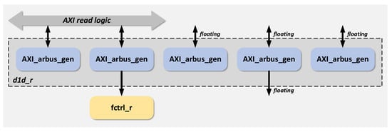
Figure 20.
Schematic diagram of D1D_R module structure.
The structural block diagram of the D1d_w module and its peripheral circuit connection relationships are shown in Figure 21.
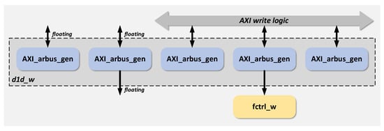
Figure 21.
Schematic diagram of D1D_W module structure.
The axi_ar/wbus_gen module implements the AXI address read/write channel logic, instantiating the same generic design module for both read and write operations. The axi_bbus_gen module handles the AXI write response channel logic, while the axi_rbus_gen and axi_wbus_gen modules implement the AXI read data and write data interface logics, respectively. When the generic d1d module is instantiated as d1d_r, the output ports of the three write-related channels are left unconnected, and their input ports are tied to constant values. Conversely, when instantiated as d1d_w, the output ports of the two read-related channels are unused, and their input ports are also tied to constants.
4.4. Xdma_Reg Module
This module is responsible for register configuration. Specifically, when using the DMA engine for data access operations, it is necessary to provide a series of parameters such as AXI read/write data length and AXIS read/write data length, configure pulse signals related to the DMA engine’s operation (e.g., xdma_start_r/w), and read status information such as whether the internal FIFO of the DMA engine is empty and whether there are errors in the read/write bus. All the above operations are implemented by reading and writing the registers declared in the DMA engine’s XDMA_reg module. The specific contents of the registers provided by this DMA engine are shown in Table 5.
Table 5.
Register list of XDMA engine (partial).
5. Experimental Testing and Results
In this section, we conduct sufficient experiments to test and evaluate the performance of the DMA engine proposed in this paper. To ensure the integrity and comprehensiveness of the experimental evaluation results, in addition to separately testing performance indicators such as the transmission rate of the DMA engine, we also embed the DMA engine into a complete FPGA-based SAR imaging processing platform in the form of an IP core to carry out performance testing on the complete imaging process. The evaluation of the experimental results is divided into two parts in total:
The first part performs module-level performance evaluation on the DMA engine, first conducting comprehensive implementation in Vivado tools to obtain the hardware resource situation of the DMA engine and comparing it with pl330w_DMA, and in addition, by writing test stimulus files, carrying out simulation tests on the DMA engine on the Verdi simulation platform to obtain the data read/write bandwidth and read/write efficiency of the DMA engine in each typical application scenario, and making horizontal comparisons with the relevant performance indicators of pl330w_DMA under the same working scenarios to conduct performance analysis and evaluation on the proposed DMA engine.
The second part performs performance testing on the SAR imaging processing platform including the DMA engine, in this part, according to the complete imaging process of the CS algorithm imaging, using the FPGA-based SAR imaging processing platform to process the SAR raw echo data, by replacing the DMA engine instantiated and used in the SAR imaging processing platform, testing and obtaining the imaging test timeliness based on different DMA engines, and making horizontal comparisons between the measured multiple groups of imaging timeliness and the imaging time in other papers to analyze and obtain the performance improvement in the proposed DMA engine for the complete SAR imaging processing platform.
The specific experimental settings and detailed experimental results will be described in the following subsections.
5.1. Experimental Setting
The hardware experimental platform selected in this paper is the VeriTiger-V19P from Yake Hongyu, as shown in Figure 1. The VeriTiger-V19P is a relatively mature FPGA prototype verification system from Hypersilicon, designed based on Xilinx’s Virtex UltraScale+ XCVU19P FPGA [39]. It supports high-performance inter-board connections through GTY high-speed transceivers and enables fully automatic and intervenable logical partitioning through self-developed partitioning tools to reasonably allocate FPGA resources. In addition, it extends memory scalability. Besides two on-board DDR4 SO-DIMM slots supporting 72-bit DDR4 with ECC functionality, it also supports two externally expanding DDR3/4 daughter cards via HSPI2-DQS and HSPI2-CAC connectors. The entire system supports the design verification of 48 million ASIC gates, provides 1644 high-performance I/Os and 36 Lane GTY channels, supports high-speed interfaces such as PCIe/SFP/Rapid IO, and has exceptional expandability. It offers over 100 fully verified functional daughter cards for verifying applications such as various SoCs, high-speed interfaces, multimedia, and artificial intelligence acceleration algorithms. These features fully meet the testing requirements of the DMA engine and the entire SAR imaging system in this paper [40].
In the complete experimental environment, a host computer is used to program the complete FPGA hardware code of the SAR imaging platform into the VeriTiger-V19P and input raw spaceborne SAR echo data into the DDR4 for subsequent experiments. The host computer can also read the processed imaging data from the DDR4. Additionally, the host computer can develop and debug the ARM processor in the hardware experimental platform through ARM (Cambridge, UK)’s official emulator: DSTREAM [41], whose physical diagram is shown in Figure 22.
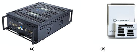
Figure 22.
The equipment used in the experimental testing. (a) The physical images of VeriTiger-V19P and (b) DSTREAM.
The software platforms for the experiments are ARM ds_IDE 2022.1, ProtoWizard-Partition 1.0.16.28, and Vivado 2022.2. ARM ds_IDE 2022.1 is responsible for the application development and debugging of the ARM processor, Vivado 2022.2 handles the development, synthesis, and implementation of hardware logic codes and generates bitstream files, and ProtoWizard-Partition 1.0.16.28 configures the power supply voltage, clock frequency, etc. of the hardware experimental platform and programs the bitstream files generated by Vivado into the platform. After the development and compilation of the software and hardware codes are completed, they are transferred from the host computer to the experimental platform via the JTAG interface for testing. It should be noted that the simulation and testing data related to the XDMA engine were all conducted under the conventional clock frequency of 200 MHz. According to the actual measurement, the maximum operating frequency of the XDMA engine deployed on the FPGA is approximately 250 MHz. Beyond this frequency, a certain degree of timing violation occurs. Based on past practical project experience, a clock frequency of 200 MHz is sufficient to meet the existing on-board processing performance requirements.
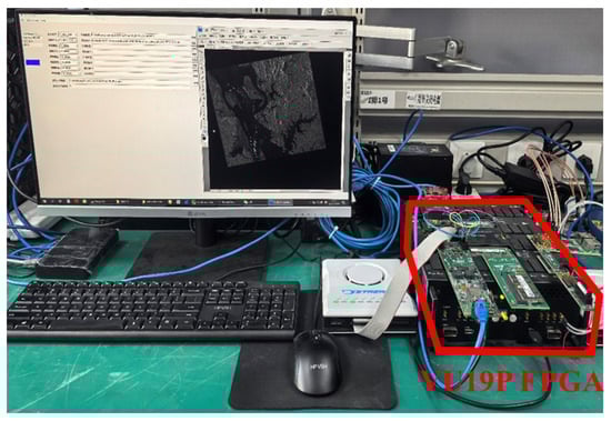
Figure 23.
Actual photo of the experimental environment.
For the FPGA-based SAR imaging processing system, we design a simplified imaging-level experimental test flow based on the algorithmic content of the standard CS (Chirp Scaling) imaging algorithm. The schematic diagram is shown in Figure 24.
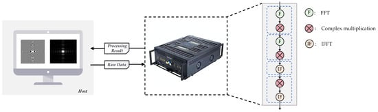
Figure 24.
Schematic diagram of the complete imaging test process.
5.2. DMA Engine Module-Level Test Results
5.2.1. Hardware Resource Utilization
The hardware resource utilization of the DMA engine, obtained by synthesizing the logic code in Vivado 2022.2, is presented in Table 6.
Table 6.
Resource utilization statistics of XDMA engine FPGA implementation.
Using the same method, the resource utilization of the ARM pl330w_DMA is shown in Table 7.
Table 7.
Resource utilization statistics of ARM pl330w_DMA engine FPGA implementation.
Table 6 and Table 7 show the resource utilization of the two DMA engines for CLB LUTs, CLB Registers, and other resources. In the tables, “Utilization” represents the quantity of a specific type of logic resource used by the DMA engine, “Available” denotes the total number of each resource type in the FPGA chip of the VeriTiger-V19P platform, and “Utilization (%)” is the ratio of the quantity of each resource used by the DMA engine to the total quantity of that resource in the FPGA chip.
As can be seen from the specific contents of the above two tables, compared with the general-purpose DMA engine ARM pl330w_DMA, the DMA engine proposed in this paper significantly reduces the usage of three hardware resources: CLB LUTs, CLB Registers, and F7&F8 Muxes. This indicates that, while improving specialization, the DMA engine eliminates redundant functions rarely used in spaceborne SAR real-time imaging scenarios, effectively reducing the scale of logic resource usage. The reduction in logic scale not only saves limited logic resources in the on-board environment but also simplifies the engine design, reduces complexity, and improves reliability. Additionally, it lowers power consumption, reduces heat generation, and enhances timing performance, offering a series of advantages for on-board application environments.
Furthermore, it can be observed that the CARRY8 usage of the XDMA engine is slightly higher than that of the ARM pl330w_DMA, reflecting the higher demand for internal addition and subtraction operations in the XDMA engine due to the presence of address jump-related instructions such as INS_ADDADDR. The use of more CARRY8 resources provides the XDMA engine with faster instruction execution speed and more flexible data reading methods, making it more suitable for high-efficiency and high-throughput application scenarios in spaceborne SAR real-time imaging processing.
From the table, it can also be observed that the ARM pl330w_DMA employs eight Block RAM Tiles, whereas the XDMA engine does not utilize any, which reflects the design strategy of the XDMA engine to conserve cache resources and reduce power consumption.
Additionally, as a data transmission engine, the DMA does not require high-speed multiplication, accumulation, or other operations. Therefore, it does not need the URAM to provide fast dual-port storage access capabilities, nor does it require the DSP to provide high-speed and complex mathematical operation capabilities. Consequently, the usage quantities of both URAM resources and DSP resources by the above two DMA engines are both zero.
5.2.2. Engine Bandwidth Performance Analysis
We conducted simulation tests on the DMA engine using the Verdi simulation platform. By analyzing the simulation waveforms, we obtained the data access bandwidth and efficiency of the DMA engine under various typical application scenarios.
Taking the data cropping operation as an example, we created test stimulus files based on the operational requirements and performed data transmission simulations on both the AXI-AXIS and AXIS-AXI channels of the XDMA engine. The specific data flow is illustrated in Figure 25.
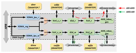
Figure 25.
Schematic diagram of simulation test data flow.
The simulation waveform diagrams are shown in Figure 26, Figure 27 and Figure 28. It should be noted that all data transmitted through the AXIS-AXI channel during the test were set to 0.
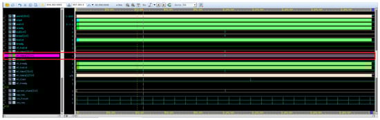
Figure 26.
Simulation diagram of data channel in AXIS-AXI data path.
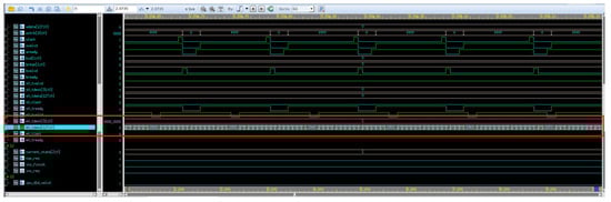
Figure 27.
Simulation diagram of data channel in AXI-AXIS data path.
Figure 28.
Simulation waveform diagram of cntr recording data volume transmitted by two data channels.
From the above three figures, it can be observed that, during the 10 ms test period, the XDMA engine transmitted a total of 1B_2067 numbers and received 18_6AF7 numbers in the test scenario. Converting these hexadecimal values to decimal, the engine transmitted 1,777,767 numbers and received 1,600,247 numbers. For the data transmission channel, the bandwidth can be calculated as follows:
1,777,767 × 16/10 ms × 1000/1024/1024/1024 ≈ 2.649 GB/s
Similarly, for the data reception channel, the bandwidth can be calculated as follows:
1,600,247 × 16/10 ms × 1000/1024/1024/1024 ≈ 2.385 GB/s
For both the data transmission and reception channels, at an operating frequency of 200 MHz, the theoretical maximum access bandwidth of the XDMA engine’s standard AXI interface with a bit width of 16 bytes is as follows:
16 × 200 × 1000 × 1000/1024/1024/1024 ≈ 2.9802 GB/s
Based on the actually measured bandwidth of the channels and the calculated theoretical maximum access bandwidth, the data access efficiencies of the transmission and reception channels can be calculated as follows:
2.649/2.9802 × 100% ≈ 88.89%
2.385/2.9802 × 100% ≈ 80.03%
Under the same test scenario, we used the same test stimuli to simulate the ARM pl330w_DMA, and the resulting waveform diagram is shown in Figure 29. The pl330w_DMA uses a set of dmareq/dmaclr signals to handshake with other IPs. Therefore, by counting the number of handshakes of the dmareq/dmaclr signals in the simulation waveform, we can obtain the quantity of data transmitted during the simulation period. It should be noted that, since the pl330w_DMA has only one set of data access interfaces based on the standard AXI3 protocol, there is only a single AXI-AXI test channel during its simulation testing.
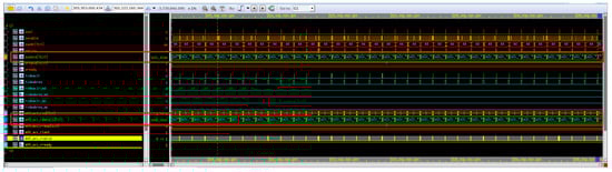
Figure 29.
Simulation diagram of data channel in AXI-AXI data path.
Based on the above simulation waveform diagrams, we can count that the pl330w_DMA transmitted a total of 1,208,114 numbers during the 10 ms simulation test period. Therefore, the data transmission bandwidth of the pl330w_DMA can be calculated as follows:
1,208,114 × 16/10 ms × 1000/1024/1024/1024 ≈ 1.8002 GB/s
For the same operating frequency and channel data bit width, the theoretical maximum access bandwidth of the pl330w_DMA’s standard AXI interface is also 2.9802 GB/s. Therefore, its data access efficiency can be calculated as follows:
1.8002/2.9802 × 100% ≈ 60.41%
Summarizing the above data, Table 8 is presented as follows.
Table 8.
Statistical comparison of bandwidth and data access efficiency between XDMA engine and PL330W.
The above experimental test data show that, in application scenarios with extensive address jumps in spaceborne SAR imaging processing, represented by transpose operations and cropping operations, the spaceborne SAR on-board real-time imaging DMA engine based on a dedicated instruction set proposed in this paper exhibits high data access bandwidth and data access efficiency, with indicators meeting imaging requirements. Compared with the traditional ARM pl330w_DMA engine based on a general-purpose instruction set, it demonstrates significant performance improvements.
In addition, the comparison of specific data transmission waveforms is shown in Figure 30.
Figure 30.
Transmission waveform comparison of two DMA Models. (a) Simulation results of the XDMA engine operation. (b) Simulation results of the pl330w_DMA engine operation.
As shown in Figure 30, during data transmission by the XDMA engine using the dedicated instruction set, the instructions are configured at the initial stage of the transmission task, and subsequent continuous data transmission begins without waiting for other configuration instructions, with the data transmission approaching cycle-by-cycle transmission. This reflects that the data transmission of the XDMA engine is not restricted by instruction configuration and has extremely high data access efficiency, enabling the XDMA engine to exhibit excellent performance in handling high-frequency and large-scale streaming data transmission tasks. In contrast, the pl330w_DMA has obvious pause waiting times during data transmission, showing a discrete and non-continuous transmission characteristic. The data transmission process of the pl330w_DMA engine can be regarded as a collection of independent transmission operations, with obvious clock cycle intervals during their execution. This is because the pl330w_DMA engine continuously performs instruction configuration during data transmission, and data transmission pauses and waits during each instruction configuration period. The data transmission speed of the engine is restricted by instruction configuration behavior, which seriously affects the data access efficiency of the engine.
Based on the above simulation test results and theoretical analysis, it can be concluded that the XDMA engine based on the dedicated instruction set not only meets the requirements of high data access bandwidth and high data access efficiency in specific application scenarios of spaceborne SAR imaging processing but also provides more excellent data access performance than the traditional ARM pl330w_DMA engine based on the general-purpose instruction set while significantly reducing the use of hardware resources. This reflects the great advantages of XDMA in the application of specific fields of spaceborne SAR imaging processing and demonstrates the significance of designing a dedicated instruction set.
5.3. SAR Imaging System Test Results
To ensure the comprehensiveness and completeness of the experimental test results, we embedded the DMA engine proposed in this paper and the ARM_pl330w DMA as IP cores into the entire FPGA-based SAR imaging processing platform, respectively, for full-process imaging experimental tests, aiming to evaluate the improvement in the XDMA engine on the overall imaging timeliness performance of the SAR imaging processing platform.
According to the designed experimental test process, we conducted SAR imaging processing experiments. In the experiments, the SAR raw echo data with a granularity of 16,384 × 16,384 was provided by the Taijing-401 satellite [42]. The SAR imaging results are represented by 8-bit grayscale images, with pixel grayscale values ranging from 0 to 255. The imaging test results and the imaging processing times of other latest SAR imaging processing systems are summarized in Table 9. When actually using the XDMA engine, if the size of the image being processed is inconsistent with the image size in the table, the time can be scaled proportionally in a linear manner. This is because the basic principle of on-board radar imaging algorithms is to split the image to be processed and handle each part sequentially. Therefore, the imaging time is linearly related to the image size.
Table 9.
Timeliness comparison of complete imaging process tests.
As can be seen from the data in the table above, compared with the imaging processing systems based on other DMA engines, the SAR imaging processing system using the XDMA engine has significantly improved imaging speed and remarkably shortened timeliness in processing image data of the same size. This indicates that the SAR imaging processing system has obvious performance advantages, reflecting that the XDMA engine has greatly improved its working performance while saving a large amount of resources. This is of great significance for the development of on-board real-time processors for spaceborne SAR. In addition, we continued to use the imaging data from Taijing-401 to conduct a complete imaging process test of the system, to ensure that the XDMA engine can guarantee the system’s ability to produce complete and high-quality images. We used SAR echo data from the southern part of India’s Andaman Islands for the test, obtaining the processing results from the FPGA-based SAR imaging system and the imaging simulation results from MATLAB R2020b. We then compared these two results with the optical remote sensing images of the region, as shown in Figure 31.
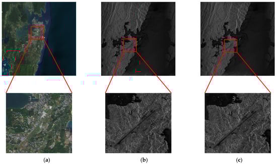
Figure 31.
Imaging result, global map optical remote sensing image, and MATLAB processing result for South Andaman Island in India. (a) Optical imaging map; (b) MATLAB imaging result; (c) FPGA imaging result (include XDMA).
From the imaging results, it can be seen that the data processing system based on the XDMA engine is capable of producing complete images with good imaging quality, high clarity, and distinguishable details. This fully validates the excellent performance of the XDMA engine.
6. Conclusions
This paper designs and implements a spaceborne SAR on-board real-time imaging processing DMA engine based on a dedicated instruction set. In the specific application scenario of spaceborne SAR on-board real-time imaging processing, this DMA engine significantly reduces hardware resource usage while remarkably improving data access bandwidth and efficiency. Experimental results show that, at a clock frequency of 200 MHz, the data reception bandwidth of this DMA engine can reach 2.385 GB/s with a reception efficiency of 80.03%, and the data transmission bandwidth can reach 2.649 GB/s with a transmission efficiency of 88.89%. Compared with traditional methods, the bandwidth is approximately 39.81% higher, demonstrating significant improvement. Additionally, compared with traditional DMA engines, the storage space occupied by operational instructions and CPU runtime of the DMA engine proposed in this study are nearly negligible when contrasted with the 10 MB storage magnitude and 1-s-order CPU time consumption of traditional schemes. Finally, the DMA engine was integrated into an FPGA-based SAR imaging processing system for imaging experimental testing to verify its improvement on the system’s imaging timeliness. The results show that, without compromising imaging quality, the DMA engine design proposed in this paper further shortens the imaging timeliness of the SAR imaging processing system. Using the CS algorithm to image a 16 k × 16 k SAR image requires only 1.2325 s, which highlights its high application value. In the future, we will continue to explore efficient DMA engine design methods for multi-channel, multi-mode, and other real-time processing scenarios based on this work to meet the needs of emerging remote sensing applications.
Author Contributions
Conceptualization, A.Z. and Y.L.; methodology, Z.Y.; software, A.Z.; validation, A.Z., M.X. and Y.L.; formal analysis, A.Z.; investigation, A.Z.; resources, Y.X.; data curation, Y.L.; writing—original draft preparation, A.Z.; writing—review and editing, M.X. and Y.X.; visualization, A.Z.; supervision, Y.X.; project administration, Z.Y.; funding acquisition, Y.X. All authors have read and agreed to the published version of the manuscript.
Funding
This work was supported by National Natural Science Foundation of China under Grant 62341130.
Data Availability Statement
The original contributions presented in this study are included in the article. Further inquiries can be directed to the corresponding author.
Conflicts of Interest
The authors declare no conflicts of interest.
References
- Raney, R.K.; Runge, H.; Bamler, R.; Cumming, I.G.; Wong, F.H. Precision SAR Processing Using Chirp Scaling. IEEE Trans. Geosci. Remote Sens. 1994, 32, 786–799. [Google Scholar] [CrossRef]
- Moreira, A.; Prats-Iraola, P.; Younis, M.; Krieger, G.; Hajnsek, I.; Papathanassiou, K.P. A Tutorial on Synthetic Aperture Radar. IEEE Geosci. Remote Sens. Mag. 2013, 1, 6–43. [Google Scholar] [CrossRef]
- Zhou, D.-M.; Gong, H.-L.; Hu, J.-M.; Wu, F.-L. Application of Satellite Remote Sensing Technology to Wetland Research. Remote Sens. Technol. Appl. 2011, 21, 577–583. [Google Scholar]
- Liu, X. Research on Key Technologies of Real time SAR Imaging Processing on the Star; Beijing Institute of Technology: Beijing, China, 2016. [Google Scholar]
- Chen, Q. Research on the Imaging Technology of Spaceborne Multimode Synthetic Aperture Radar. Ph.D. Thesis, National University of Defense Technology, Changsha, China, 2013. [Google Scholar]
- Wahl, D.E.; Eichel, P.H. Phase gradient autofocus-a robust tool for high resolution SAR phase correction. IEEE Trans. Aerosp. Electron. Syst. 1994, 30, 827–835. [Google Scholar] [CrossRef]
- Hirose, A.; Rosen, P.A.; Yamada, H.; Zink, M. Foreword to the Special Issue on Advances in SAR and Radar Technology. IEEE J. Sel. Top. Appl. Earth Obs. Remote Sens. 2015, 8, 3748–3750. [Google Scholar] [CrossRef]
- Long, T.; Zeng, T.; Hu, C.; Dong, X.; Chen, L.; Liu, Q.; Xie, Y.; Ding, Z.; Li, Y.; Wang, Y.; et al. High Resolution Radar Real-Time Signal and Information Processing. China Commun. 2019, 16, 105–133. [Google Scholar]
- Bian, M.M.; Bi, F.K.; Liu, F. Matrix transpose methods for SAR imaging system. In Proceedings of the IEEE 10th International Conference on Signal Processing Proceedings, Beijing, China, 24–28 October 2010. [Google Scholar]
- Guo, C.; Xu, J.; Xu, W. Highly efficient design of SDRAM-based CTM for real-time SAR imaging system. IET Circuits Devices Syst. 2019, 13, 656–660. [Google Scholar] [CrossRef]
- Yu, C.-L.; Chakrabarti, C. Transpose-Free SAR Imaging on FPGA Platform. In Proceedings of the 2012 IEEE International Symposium on Circuits and Systems, Seoul, Republic of Korea, 20–23 May 2012; pp. 762–765. [Google Scholar]
- Shin, H.; Kim, D.; Park, E.; Park, S.; Park, Y.; Yoo, S. McDRAM: Low latency and energy-efficient matrix computations in DRAM. IEEE Trans. Comput. Aided Design Integr. Circuits Syst. 2018, 37, 2613–2622. [Google Scholar] [CrossRef]
- Fujiki, D.; Mahlke, S.; Das, R. In-memory data parallel processor. ACM Sigplan Not. 2018, 53, 1–14. [Google Scholar] [CrossRef]
- Khunjush, F.; Dimopoulos, N.J. Extended characterization of DMA transfers on the Cell BE processor. In Proceedings of the 2008 IEEE International Symposium on Parallel and Distributed Processing, Miami, FL, USA, 14–18 April 2008. [Google Scholar]
- Wang, Z.; Wang, Z.; Liao, J.; Chen, C.; Yang, Y.; Dong, B.; Chen, W.; Chen, W.; Lei, M.; Guo, W.; et al. CNN-DMA: A Predictable and Scalable Direct Memory Access Engine for Convolutional Neural Network with Sliding-window Filtering. In Proceedings of the 2021 on Great Lakes Symposium on VLSI, Virtual Event, USA, 22–25 June 2021. [Google Scholar]
- Texas Instruments. TMS320C6000 DSP Enhanced Direct Memory Access (EDMA) Controller Reference Guide; SPRU234; Texas Instruments: Dallas, TX, USA, 2006. [Google Scholar]
- Jamshidi, D.A.; Samadi, M.; Mahlke, S. D2MA: Accelerating coarse-grained data transfer for GPUs. In Proceedings of the 23rd International Conference on Parallel Architectures and Compilation, Edmonton, AB, Canada, 23–27 August 2014. [Google Scholar]
- DMA for PCI Express (PCIe) Subsystem. Xilinx. Available online: https://www.xilinx.com/products/intellectual-property/pcie-dma.html (accessed on 16 June 2025).
- Vollmuller, G.; Algra, T.; Oving, B.; Wiegmink, K.; Bierens, L. On-Board Payload Data Processing, for SAR and Multispectral Data Processing, on-Board Satellites (LEON2/FFTC). In Proceedings of the 2nd International Workshop on OnBoard Payload Data Compression, Toulouse, France, 28–29 October 2010. [Google Scholar]
- Achim, A.; Tsakalides, P.; Bezerianos, A. SAR Image Denoising via Bayesian Wavelet Shrinkage Based on Heavy-Tailed Modeling. IEEE Trans. Geosci. Remote Sens. 2003, 48, 1773–1784. [Google Scholar] [CrossRef]
- Lovelly, T.M.; Wise, T.W.; Holtzman, S.H.; George, A.D. Benchmarking Analysis of Space-Grade Central Processing Units and Field-Programmable Gate Arrays. J. Aerosp. Inf. Syst. 2018, 15, 518–529. [Google Scholar] [CrossRef]
- Sun, T.; Xie, Y.; Li, B. Efficiency Balanced Matrix Transpose Method for Sliding Spotlight SAR Imaging Processing. J. Eng. 2019, 2019, 7775–7778. [Google Scholar] [CrossRef]
- Ma, S.; Lei, Y.; Huang, L.; Wang, Z. MT-DMA: A DMA controller supporting efficient matrix transposition for digital signal processing. IEEE Access 2018, 7, 5808–5818. [Google Scholar] [CrossRef]
- Lee, W.J.; Kim, C.H.; Paik, Y.; Kim, S.W. PISA-DMA: Processing-in-Memory Instruction Set Architecture Using DMA. IEEE Access 2023, 11, 8622–8632. [Google Scholar] [CrossRef]
- Rossi, D.; Loi, I.; Haugou, G.; Benini, L. Ultra-low-latency lightweight DMA for tightly coupled multi-core clusters. In Proceedings of the 11th ACM Conference on Computing Frontiers, New York, NY, USA, 20 May 2014. [Google Scholar]
- Ma, S.; Huang, L.; Lei, Y.; Guo, Y.; Wang, Z. An efficient direct memory access (DMA) controller for scientific computing accelerators. In Proceedings of the 2019 IEEE International Symposium on Circuits and Systems (ISCAS), Sapporo, Japan, 26–29 May 2019. [Google Scholar]
- Franceschetti, G.; Lanari, R. Synthetic Aperture Radar Processing; CRC Press: Boca Raton, FL, USA, 2018. [Google Scholar]
- Nedbailo, Y.A.; Petrov, I.A. Increasing DDR4 SDRAM throughput in parallel workloads. In Proceedings of the 2020 Moscow Workshop on Electronic and Networking Technologies (MWENT), Moscow, Russia, 11–13 March 2020. [Google Scholar]
- Zhang, H.; Zhang, Z.; Gong, Y.; Zhang, Y.; Jung, J.; Lee, B.; Kim, E.; Cao, K. A Data Eye Width Improved and ODT PVT Tolerance Enhanced DDR4 SDRAM Using Fast Clock Gating and tADC Self-align. In Proceedings of the 2021 6th International Conference on Integrated Circuits and Microsystems (ICICM), Nanjing, China, 22–24 October 2021. [Google Scholar]
- Zheng, J.; Yan, K.; Zhang, Y.; Chen, Z. Design and implementation of DDR4 SDRAM controller based on FPGA. In Proceedings of the 2018 2nd IEEE Advanced Information Management, Communicates, Electronic and Automation Control Conference (IMCEC), Xi’an, China, 25–27 May 2018. [Google Scholar]
- Priyanka, B.; Kumar, B.A.; Kumar, D.S. High Coverage DDR4 SDRAM Memory Design and Verification Using System Verilog and UVM. In Proceedings of the 2024 2nd International Conference on Cyber Physical Systems, Power Electronics and Electric Vehicles (ICPEEV), Hyderabad, India, 26–28 September 2024. [Google Scholar]
- Kim, W.; Bae, D.; Khan, S.A.; Kih, J.; Chung, S.S.; Son, S.; Kim, H.; Eom, D.; Woo, S.; Kim, J.; et al. Effects of Proton and Gamma Radiation on DDR4 SDRAM in Elevated Temperature. In Proceedings of the 2024 RADECS Data Workshop, Maspalomas, Spain, 19 September 2024. [Google Scholar]
- Yuan, D.; Yang, Y.; Liu, X.; Zhang, G.; Chen, J. A data dependency based strategy for intermediate data storage in scientific cloud workflow systems. Concurr. Comput. Pract. Exp. 2012, 24, 956–976. [Google Scholar] [CrossRef]
- Wang, G.; Chen, H.; Xie, Y. An efficient dual-channel data storage and access method for spaceborne synthetic aperture radar real-time processing. Electronics 2021, 10, 662. [Google Scholar] [CrossRef]
- Li, B.; Shi, H.; Chen, L.; Yu, W.; Yang, C.; Xie, Y.; Bian, M.; Zhang, Q.; Pang, L. Real-time spaceborne synthetic aperture radar float-point imaging system using optimized mapping methodology and a multi-node parallel accelerating technique. Sensors 2018, 18, 725. [Google Scholar] [CrossRef] [PubMed]
- Akin, B.; Franchetti, F.; Hoe, J.C. FFTS with near-optimal memory access through block data layouts. In Proceedings of the 2014 IEEE International Conference on Acoustics, Speech and Signal Processing (ICASSP), Florence, Italy, 4–9 May 2014; pp. 3898–3902. [Google Scholar]
- CoreLink DMA-330: High-Performance Data Transfer—Arm®. Available online: https://www.arm.com/products/silicon-ip-system/embedded-system-design/dma-330 (accessed on 16 June 2025).
- AMBA Specifications—Arm®. Available online: https://www.arm.com/architecture/system-architectures/amba/amba-specifications (accessed on 16 June 2025).
- Virtex UltraScale+ VU19P FPGA. Available online: https://www.amd.com/zh-cn/products/adaptive-socs-and-fpgas/fpga/virtex-ultrascale-plus-vu19p.html (accessed on 16 June 2025).
- Yakohongyu EDA|Accelerating SoC/ASIC Simulation and Verification|Leading Provider of Prototyping and Emulation Solutions. Available online: http://www.hypersilicon.com/yahong/news/detail.html?id=25 (accessed on 16 June 2025).
- DSTREAM-ST|High-Performance Arm Debug and Parallel Trace—Arm®. Available online: https://www.arm.com/products/development-tools/debug-probes/dstream-st (accessed on 16 June 2025).
- Taijing-4 01, 02, 03. Available online: https://space.skyrocket.de/doc_sdat/taijing-4.htm (accessed on 16 June 2025).
- Wang, Y.; Li, W.; Liu, T.; Zhou, L.; Wang, B.; Fan, Z.; Ye, X.; Fan, D.; Ding, C. Characterization and implementation of radar system applications on a reconfigurable dataflow architecture. IEEE Comput. Archit. Lett. 2022, 21, 121–124. [Google Scholar] [CrossRef]
- Lin, J.Z.; Chen, P.T.; Chin, H.Y.; Tsai, P.Y.; Lee, S.Y. Design and implementation of a real-time imaging processor for spaceborne synthetic aperture radar with configurability. IEEE Trans. Very Large Scale Integr. (VLSI) Syst. 2023, 32, 669–681. [Google Scholar] [CrossRef]
Disclaimer/Publisher’s Note: The statements, opinions and data contained in all publications are solely those of the individual author(s) and contributor(s) and not of MDPI and/or the editor(s). MDPI and/or the editor(s) disclaim responsibility for any injury to people or property resulting from any ideas, methods, instructions or products referred to in the content. |
© 2025 by the authors. Licensee MDPI, Basel, Switzerland. This article is an open access article distributed under the terms and conditions of the Creative Commons Attribution (CC BY) license (https://creativecommons.org/licenses/by/4.0/).