Article

Digital Control of a Bidirectional Resonant Converter for Electric Vehicle Applications with Enhanced Transient Response

1
Department of Electrical Engineering, Ming Chi University of Technology, New Taipei City 243303, Taiwan
2
Organic Electronics Research Center, Ming Chi University of Technology, New Taipei City 243303, Taiwan
*
Author to whom correspondence should be addressed.
Electronics 2025, 14(16), 3202; https://doi.org/10.3390/electronics14163202
Submission received: 2 July 2025 / Revised: 7 August 2025 / Accepted: 8 August 2025 / Published: 12 August 2025
(This article belongs to the Special Issue Advanced Technologies in Power Electronics)

Abstract

This paper presents the design and implementation of a bidirectional resonant converter with enhanced dynamic response to electric vehicles (EV). The proposed system comprises an assembly of four switches, a capacitor, and an inductor on both the primary and secondary sides of the transformer. The value of C-L-L-C was calculated using the first harmonic approximation method. Moreover, the small-signal analysis method was used to design the control system and analyze the dynamic performance of the system. Closed-loop control algorithms for voltage and current loops with synchronous rectifiers (SRs) were designed and implemented on a 32-bit microcontroller (STM32G474RET6). A 70 kHz, 400 W prototype is built with a peak conversion efficiency of 95.05% using SR in the forward mode. Without SR, the peak conversion efficiency was 93.57% in the forward mode and 93.04% in the reverse mode. In the forward mode, the proposed algorithm reduced the settling time to 15 ms, in contrast to the 40 ms associated with the conventional algorithm; in the reverse mode, the proposed algorithm reduced the settling time to 10 ms, in contrast to the 15 ms associated with the conventional algorithm.

1. Introduction

Electric vehicles are becoming more widely used due to their low emissions. Electric vehicle systems comprise an on-board charger that converts grid voltage into a voltage suitable for charging electric vehicle batteries [1]. Presently, these on-board chargers are required to provide charging functionality and operate in the reverse operation mode. In the reverse operation mode, the battery can simultaneously release energy to AC loads or to the grid that supplies power to other electric vehicles. Electric vehicle batteries can function as distributed power sources to smoothen fluctuations in energy demand from the grid. Figure 1 displays a schematic of a typical electric vehicle system comprising a filter cascaded with an AC-DC converter and a DC-DC converter. The AC-DC converter requires a high power factor and often uses power factor correction. The DC-DC converter provides the isolation required to ensure safety during vehicle charging. Among DC-DC converters, the CLLC converter is becoming increasingly popular because it can achieve maximum efficiency and soft switching across the full load range [2].
CLLC converters can operate under soft switching conditions for primary switches and secondary rectifiers. In addition, the voltage stresses of the power switches are confined to the input and output voltage without any clamping circuits. The operation of CLLC converters differs between the forward and reverse power conversion modes because of the asymmetric turn ratios and the structure of resonant networks with the transformer. Several studies have explored the design and control of CLLC converters, especially focusing on bidirectional and resonant converters. For instance, recent research has highlighted advanced control methods to enhance the dynamic response and improve the converter’s performance under varying load conditions [3]. However, limited studies have provided a comprehensive approach that ensures high efficiency during bidirectional operation while addressing practical challenges such as component size, thermal management, and complexity control. Some researchers have proposed adaptive control methods, such as model predictive control and artificial intelligence-based techniques, to optimize the response time of resonant converters under varying load and voltage conditions [4]. These approaches focus on rapid settling times while maintaining efficiency and ensuring reliable operation across a wide range of operating scenarios. Bidirectional converters operate at a diverse range of voltages and relatively high efficiency. As their name suggests, they are capable of transferring power in both directions [5]. Bidirectional converters have risen in prominence as a topic of research in power electronics because of their extensive range of applications, including wind farms, electric vehicles, aircraft, uninterruptible power supply, solar farms, X-ray, and military applications [5]. Recent studies have also explored combining conventional control strategies, such as phase-shift modulation, with state-plane trajectory control to improve the dynamic response, particularly under transient conditions [6]. These hybrid solutions offer a balance between simplicity and improved transient performance, providing a viable pathway for optimizing converters in modern applications.
Resonant converters operate on the principle of circuit resonance [7]. Resonance occurs in a circuit when the inductive reactance is equal to the capacitive reactance. At resonance, both the inductor, which stores magnetic energy, and the capacitor, which stores electrical energy, charge and discharge energy continuously. Resonant converters contain resonant LC networks whose voltage and current waveforms vary sinusoidally during one or more subintervals of each switching period. Resonant converters induce soft switching with LC elements. Resonant converters can be classified into three types: series, parallel, and series–parallel hybrid [8]. CLLC converters belong to the series–parallel hybrid type of resonant converters. Recent works have also explored novel resonant converter topologies to further optimize efficiency and voltage regulation [9].
Five methods are commonly used for controlling CLLC converters: frequency modulation (FM) control, phase-shift modulation (PSM) control, self-sustained oscillation control, self-sustained PSM control, and optimum control [10]. Each of these methods has some benefits and some drawbacks. FM control, which is often employed to preserve zero-voltage switching (ZVS), requires wide frequency variation [11]. The converter is considerably derated because of the operating frequency, which is far more than the resonant frequency. Furthermore, tuning of the magnetic components and gate driver circuitry becomes challenging because of the notable frequency fluctuation. Overall, the huge size of power circuit components and reduced efficiency are the drawbacks of FM control in resonant converters. Conversely, PSM control enables fixed-frequency control methods, such as ZVS capability and the constant frequency functioning of the converter. However, under conditions of a light load and a broad input voltage range, all switches fail to maintain ZVS [12]. A hybrid controller, often referred to as a mixed controller, was proposed to address the shortcomings of both the FM and PSM control methods [5]. At low power levels, the hybrid controller locks the frequency at a maximum predetermined value and utilizes the PSM controller to prevent operations at frequencies well above the resonant frequency. At medium-to-high power levels, the hybrid controller leverages the traditional FM controller to operate within a limited range of fluctuating frequencies. However, the hybrid control method is complicated by the presence of two controllers. A previous study demonstrated the real-world applicability of this hybrid control strategy by adopting a fixed-frequency PSM method for CLLC converters [10]. This method is preferred when the converter maintains a constant output voltage at a fixed switching frequency. Nevertheless, its major drawback is the inability to effectively control converters operating over a wide output voltage range. To address this limitation, the FM method operates in conjunction with the PSM method to regulate the output voltage under conditions of low output voltage and a light load [11]. In the present study, the proposed method associates the specific output voltage with the switching frequency, thereby improving control flexibility. Additionally, the FM method can be combined with a synchronous rectifier (SR) for a low-voltage energy storage system [12]. The advantage of the proposed method is that it employs an SR for mitigating conduction losses in the switches and for increasing efficiency in the forward and reverse modes. Furthermore, state-plane trajectory control can be used as a variable frequency controller in resonant converters. It provides extremely rapid transient responses and inherent protection against the overcurrent. However, it resembles the all-state feedback control approach in that it requires the measurement of every converter state. Optimum control is regarded as a particular instance of state-plane trajectory control wherein the controller follows a certain path while maintaining the resonant tank energy within predetermined bounds [13]. Load resonant converters are a type of variable frequency controller that perform better than FM controllers because they operate at a lower frequency. Recent investigations have also introduced machine learning algorithms to enhance real-time performance and adapt to varying load conditions, which represents another promising avenue of innovation [14].
In response to the recent literature on adaptive and AI-based control strategies for bidirectional resonant converters [3,4,6,9,11,13,14], the proposed gain-compensated PI loop has been comparatively analyzed in terms of speed, robustness, and implementation complexity. Table 1 summarizes the comparison among various control techniques. While the proposed method may not achieve the ultra-fast response of AI or MPC-based techniques, it offers an optimal trade-off between control performance and system simplicity, making it particularly suitable for real-time embedded applications with constrained resources.
Recent developments in digital control for resonant converters, particularly in electric vehicle (EV) systems, have introduced machine learning techniques, model predictive control (MPC), and advanced nonlinear controllers to enhance system response, robustness, and adaptability [3,15,16]. These approaches aim to address challenges in rapid load fluctuations, such as those experienced during regenerative braking or sudden acceleration in EVs. Compared to traditional CLLC converters, other resonant topologies such as LLC, LCC, and Dual-Active-Bridge (DAB) converters have also been explored for high-efficiency, high-power density applications [15,17]. While the CLLC provides inherent bidirectional capability and ZVS/ZCS operation, other topologies may offer improved control simplicity or integration with battery management systems (BMS). Modern EV architectures increasingly demand compatibility with vehicle-to-grid (V2G) interfaces, smart charging protocols, and CAN-based communication. Integrating resonant converters with such systems requires controllers to support fast communication, predictive adaptation, and fault-tolerant operation [18]. Although PI controllers are widely used for their simplicity and implementation ease on microcontrollers, alternative strategies such as sliding mode control, deadbeat control, and adaptive feedback linearization are gaining attention due to their robustness against parameter variation and nonlinearity [3,19].
In particular, CLLC converters are increasingly employed in electric vehicle systems for high-efficiency power transfer. In such applications, the load variation in the CLLC converter occurs during braking or acceleration of the electric vehicle system. In fact, the CLLC converter must adapt and regulate the output voltage to a nearly stable value while the load varies. Most authors have used the first harmonic approximation (FHA) to analyze the characteristics of voltage gain and design of the control system, but the FHA cannot describe the dynamic response of the system [13].
In modern electric vehicles, a fast dynamic response in power converters is crucial to ensure stable and reliable operation during events such as rapid acceleration, regenerative braking, and transitions between charging and discharging modes. A sluggish control response can result in voltage instability, increased stress on components, and inefficient energy transfer. While several studies have investigated bidirectional CLLC converters, many of them have not achieved the fast dynamic response required for electric vehicle (EV) applications under rapidly changing load conditions [3,5]. Moreover, existing digital control strategies are often constrained by implementation complexity or hardware limitations [12]. To address these gaps, this study proposes a gain-compensated control algorithm designed to improve the settling time of the CLLC converter while maintaining practical simplicity for real-time implementation. The proposed gain-compensated control algorithm improves the converter’s transient response, allowing it to adapt more quickly to sudden load changes while maintaining a high efficiency. This makes the method particularly well-suited for on-board EV chargers and bidirectional energy interfaces, where both performance and reliability are critical. By addressing a key control challenge, this work contributes to the development of more robust and responsive power systems for future EV applications.

2. Operating Principles

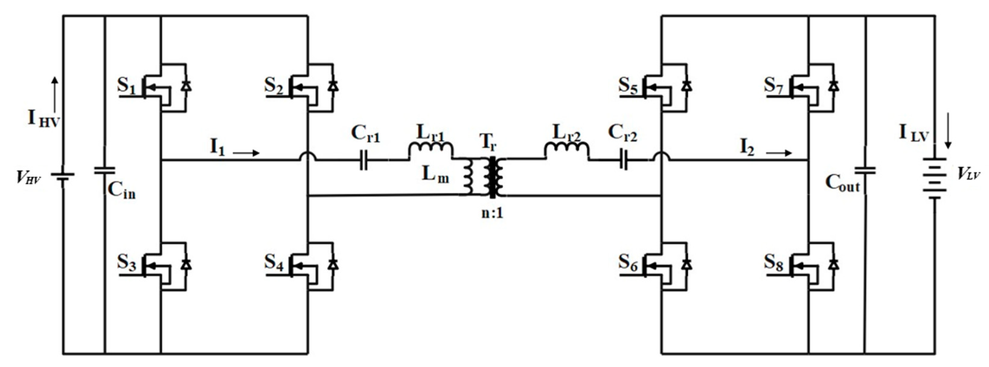
Figure 2 illustrates the configuration of the CLLC converter. In Figure 2, V H V and I H V   denote the voltage and current at the high voltage side, respectively;   I 1 denotes the primary current;   S 1 S 4 denote the primary switches; S 5 S 8 denote the secondary switches; C r 1 and C r 2 denote the resonant capacitors; L r 1 and L r 2 denote the resonant inductors; L m denotes the magnetizing inductor; I 2   denotes the secondary current; C i n and   C o u t denote the input and output capacitors, respectively; and   V L V denotes the voltage at the low voltage side.
The converter can operate in the forward or reverse operating mode. In the forward mode, power is converted from the primary to the secondary side, and the output voltage is lower than the input voltage with the purpose of charging the battery. In the reverse mode, power is converted from the secondary to the primary side, and the output voltage is greater than the input voltage with the purpose of releasing energy from the battery.
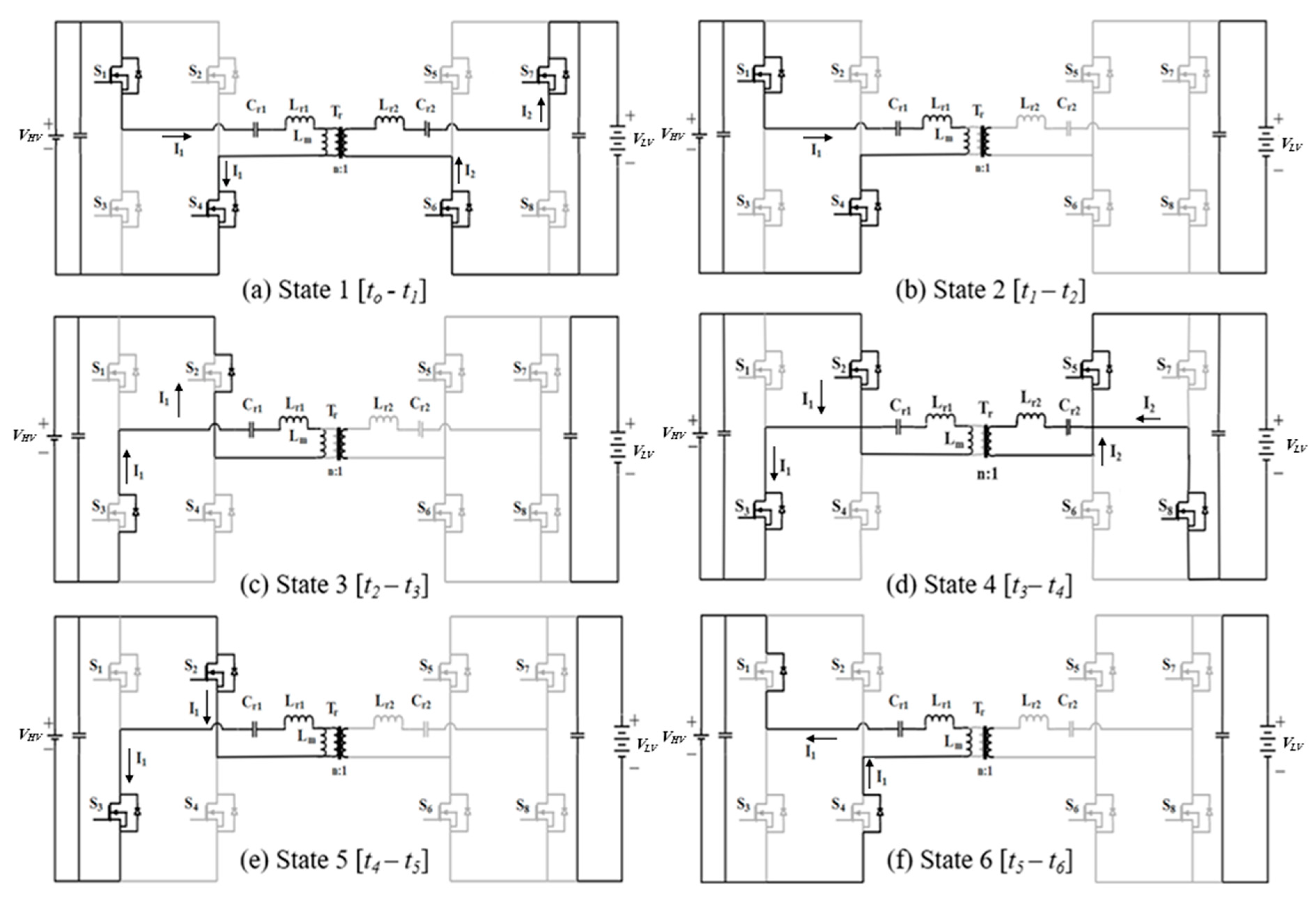
Figure 3 depicts the operating states of the proposed CLLC converter. The converter operates in six states during a switching cycle. States 1, 2, and 3 are operated repeatedly with various pairs of switches and rectifiers to achieve States 4, 5, and 6. States 1 and 4 are modes of resonance and power transfer, States 2 and 5 are modes of non-resonance, and States 3 and 6 represent the dead-time duration. The switches on the primary side function in the forward mode when energy is converted from the primary to the secondary side, whereas the switches on the secondary side are turned off and function as rectifiers. In the figure, the red and blue arrows indicate the current flow on both sides of the converter (I1 and I2, respectively), clearly showing how energy is transferred through the transformer (Tr). The voltage boosting process occurs as the secondary-side current is reflected to the primary side according to the transformer turns ratio, demonstrating the step-up conversion capability of the CLLC topology.
State 1 [ t 0 t 1 ]: S 1 and S 4 are turned on, and power is converted to the secondary rectifying stage through the transformer T r . The input voltage source V H V forces the primary currents to flow in the positive direction through S 1 and S 4 . The output voltage on the secondary side is induced on the magnetizing inductor L m , leading to the linear buildup of the magnetizing current I m . Therefore, L m does not participate in the resonance of the primary side.
State 2 [ t 1 t 2 ]: The resonance is broken, and power is no longer converted to the secondary side when I 1 drops to I m . The primary current I 1 is equal to the magnetizing current I m during this mode, and the magnetizing energy is built up until the switches S 1 and S 4 are turned off. During this period, L m participates in the resonant operation because the output stage is separated from the primary side. The resonant tank is configured such that L m is in series with L r 1 and C r 1 . In State 2, I 1 follows I m with a large magnetizing inductance, so its resonance can be ignored.
State 3 [ t 2 t 3 ]: In this state, the pair of switches S 3 and S 2 are used to create a dead-time duration. Under the ZVS state, the antiparallel diodes of S 3 and S 2 conduct the current.
State 4 [ t 3 t 4 ]: The converter begins to convert power from the primary side to the secondary side when S 3 and S 2 are turned on. Similarly to State 1, I 1 changes direction throughout this mode.
State 5 [ t 4 t 5 ]: Similarly to State 2, resonance is broken in State 5, and power is no longer being converted. I 2 becomes zero in the absence of power conversion through T r .
State 6 [ t 5 t 6 ]: No power is delivered to the secondary rectifying stage during this dead-time state. The antiparallel diodes of S 1 and S 4 conduct the primary current, enabling the operation of a switch in the ZVS state.
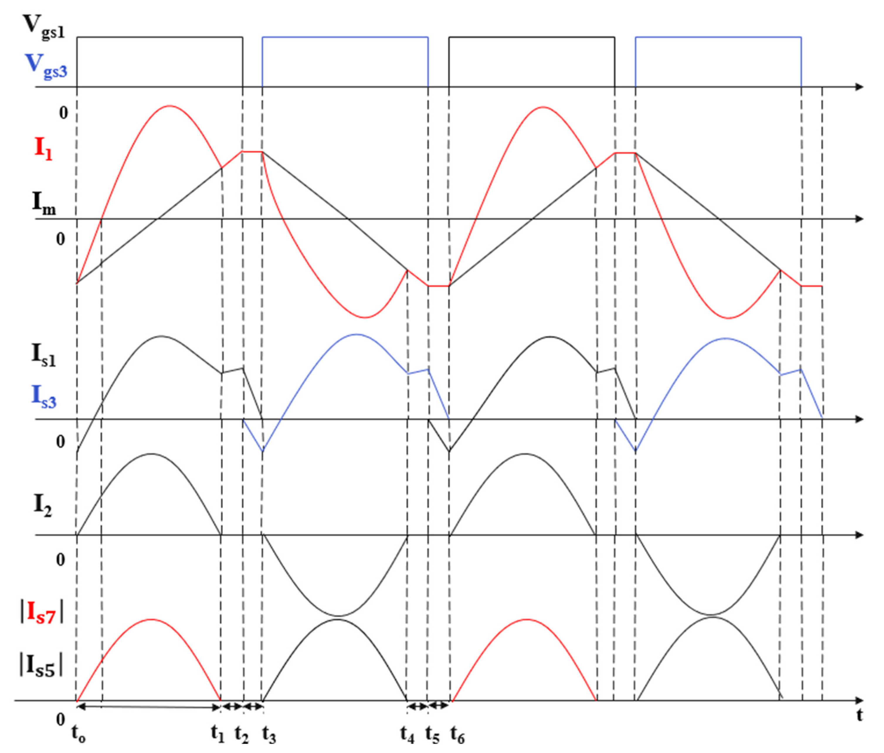
Figure 4 illustrates the theoretical waveforms for each mode during a single switching cycle. Because the configuration of the primary and secondary sides is symmetric, the waveforms of the forward and reverse modes are identical. This symmetric configuration ensures that the power conversion efficiency and the switch control method are maintained constantly regardless of the power flow direction.
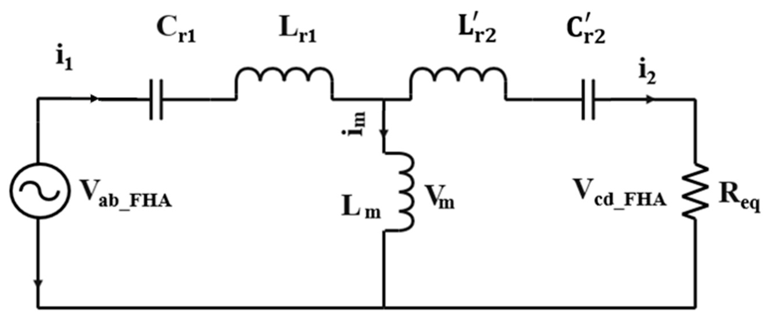
The FHA method greatly simplifies the design process. The voltage gain equation, which relates the output voltage to the input voltage as a function of switching frequency, plays an important role in the design of resonant converters. This equation has a clear physical interpretation, making it amenable for use in the design of new converters. Through the FHA method, the circuit depicted in Figure 2 can be approximated to the equivalent circuit depicted in Figure 5. The electrical circuit of the proposed converter can be simplified to obtain the gain of the resonant network with respect to the switching frequency.
The square wave can be mathematically expressed using a Fourier series as follows:
v a b _ F H A t = 4 V H V π × n = 1 . 3 . 5 . 1 n × sin 2 π n f s t
The fundamental component of v a b _ F H A ( t ) can be extracted from Equation (1) using the FHA method as follows:
v a b _ F H A t = 4 V H V π × sin 2 π f s t
where   t is the time parameter; f s is the switching frequency; and v a b _ F H A ( t ) is a square waveform that varies from V H V to V H V . The root-mean-square value of v a b _ F H A ( t ) is V a b _ F H A   , which can be calculated as follows:
V a b _ F H A = 2 2 π × V H V
Accordingly, the output voltage of the resonant network, v c d _ F H A ( t ) , can be expressed as follows:
v c d _ F H A t = 4 π   ×   V L V   ×   sin 2 π f s t
where   is the phase shift associated with the input voltage; v c d _ F H A t is a square waveform that varies from V LV to V LV . The root-mean-square value of v c d _ F H A ( t ) is V c d _ F H A   , which can be calculated as follows:
V c d _ F H A = 2 2 π   ×   V L V
The fundamental component of the rectifier current, i 2 ( t ) , can also be expressed in the same form as Equations (2) and (4) as follows:
i 2 t = 2 I 2 × sin 2 π f s t
where I 2 is the root-mean-square value of i 2 ( t ) . Therefore, the average output current, I LV , can be derived from Equation (6) as follows:
I LV = 2 T s 0 T s 2 i 2 t d t = 2 2 π × I 2
Given that v c d _ F H A ( t ) and i 2 t are in phase, the resistive load of the resonant network, R o _ e q , is equal to the ratio of the instantaneous voltage to the current with the load resistance, as shown in Equation (8).
R o _ e q = V c d _ F H A I 2 = 8 π 2 × V L V I L V = 8 π 2   ×   R o
The mathematical expression for equivalent resistance on the primary side is given in Equation (9):
R e q = n 2 R o _ e q = 8 n 2 π 2 × R o
where R o is the original load resistance in the forward mode. All the equivalent resonant parameters associated with the primary side can be derived as shown in Equation (10).
L r 2 = n 2 L r 2 ,   C r 2 = C r 2 n 2
From Equation (1), v a b _ F H A ( t ) and v c d _ F H A ( t ) can be derived in the Laplace domain as follows:
V a b _ F H A s = 4 V H V π × f s s 2 + f s
V c d _ F H A s = 4 V L V π × f s s 2 + f s
The following relations can be derived by applying Kirchhoff’s voltage law to the configuration presented in Figure 5.
V L m s = I 2 s × n 2 s L r 2 + n 2 s C r 2 + 8 n 2 π 2   ×   R o I m s = V L m s s L m 4 V H V π × f s s 2 + f s = I L m s + I 2 s × 1 s C r 1 + s L r 1 + V L m s
The expression for the equivalent output current I 2 s in the Laplace domain is presented in Equation (14). The equivalent output current in the Laplace domain can be expressed in terms of the switching frequency using Equation (13).
I 2 s = 4 V H V π × f s s 2 + f s × 1 1 s C r 1 + s L r 1 + n 2 s L r 2 + n 2 s C r 2 + 8 n 2 π 2 × R o × 1 + 1 s L m × 1 s C r 1 + s L r 1
The expression for the equivalent output voltage before the diode bridge in the frequency domain can be derived by combining Equations (9) and (14), as follows:
V c d _ F H A s =   I 2 s × R e q =   32 V H V R o n 2 π 3 × f s s 2 + f s × 1 1 s C r 1 + s L r 1 + n 2 s L r 2 + n 2 s C r 2 + 8 n 2 π 2 × R o × 1 + 1 s L m × 1 s C r 1 + s L r 1
The general transfer function M s can be determined from Equations (11) and (15) as follows:
M ( s ) = V c d _ F H A s V a b _ F H A s = 8 n 2 π 2 × R o 1 s C r 1 + s L r 1 + n 2 s L r 2 + n 2 s C r 2 + 8 n 2 π 2 × R o × 1 + 1 s L m × 1 s C r 1 + s L r 1
The gain function of the CLLC converter can be derived from Equation (16) as follows:
M s =   1 1 + 1 K 1 K f n 2 2 + Q f n × 2 + 1 K Q f n × 2 + 1 K + Q K f n 3 2
The mathematical expressions for the quality factor, inductance ratio, resonant frequency, and normalized frequency are given in Equations (18)–(22), respectively.
Q = L r 1 C r 1 R e q
K = L m L r 1
f r 1 = 1 2 π L r 1 C r 1
f r 2 = 1 2 π ( L r 1 + L m ) L r 1 = f r 1 k + 1
f n = f s f r 1
In this section, the relationship between K , Q , and f n is analyzed, and the voltage gain characteristic of the system is explained. In the next section, the mathematical expressions for calculating the value of each component, such as L r 1 , C r 1 , L r 2 , C r 2 , and L m , will be discussed.
3. Design Methodology

3.1. System Parameters Design

The CLLC converter is designed according to the specifications listed in Table 2.
The rated point is typically set to the resonance frequency, so the turns ratio n of the transformer can be obtained from Equation (23).
n = V H V _ n o m V L V _ n o m = 200 48 = 4.16
The turns ratio chosen is n = 4.
Depending on the range of input and output voltages, the maximum and minimum voltage gains can be obtained from Equation (24).
M m a x = n V L V _ m a x V H V _ m i n = 4 × 60 100 = 2.4   M m i n = n V L V _ m i n V H V _ m a x = 4 × 45 220 = 0.81  
Next, the values of K and Q must be determined [20].
The voltage gains at the maximum frequency increase as Q decreases. Therefore, ensuring that the voltage gain at the maximum frequency meets the minimum voltage gain during operation when the converter is under no load is necessary. The maximum values of the normalized frequency f n and K can be obtained by putting Q = 0 into Equation (17), as shown in Equation (25).
f n _ m a x =   f s _ m a x f r = 95   k H z 70   k H z = 1.35 k m a x = M m i n 1 M m i n × f n _ m a x 1 2 f n _ m a x 2 = 0.81 1 0.81 × 2.38 2 1 2.38 2 = 5.1
To improve efficiency and consider a margin of approximately 10%, K = 4.28 is chosen. When K remains constant, the voltage gains decrease as the value of Q increases. Given that Q attains its largest value at full load, the value of Q should be designed to ensure that the voltage gain at the minimum operating frequency meets the maximum voltage gain requirement during operation when the converter is fully loaded; therefore, the maximum value of Q can be derived from Equation (26).
Q m a x = 1 + k k . M m a x = 1 + 4.28 4.28 × 2.0 = 0.54
To improve efficiency, the value of Q should be as high as possible; therefore, Q = 0.55 is chosen.
The equivalent resistance Req of the converter must be determined, as shown in Equation (27), to design the resonant inductor and capacitor.
R e q = 8 n 2 × V L V _ n o m 2 π 2 P o = 8 × 4 2 × 48 2 π 2 × 400 = 74.70   Ω
The value of the resonant inductance on the primary side is calculated from Equation (28).
L r 1 = Q × R eq 2 π f r = 0.55 × 74.7 2 π × 70000     93   μ H
The value of the resonant capacitance on the secondary side is calculated from Equation (29).
C r 1 = 1 2 π Q R e q f r = 1 2 π × 0.55 × 74.7 × 70000     55   n F
The value of the magnetizing inductance is calculated from Equation (30):
L m = k L r 1 =   4.28   × 93     400   μ H
where n = 4. The value of the resonant inductance on the secondary side is calculated from Equation (31).
L r 2 = L r 1 n 2 = 35 uH 16     6   μ H
The value of the resonant capacitance on the secondary side is calculated from Equation (32).
C r 2 = n 2 C r 1     1   μ F
The transfer function H 2 ( s ) of the plant is presented in Equation (33).
T s = H 2 s = y s v g ^ s = N 1 s 8 + + N 8 s + N 9 D 1 s 9 + + D 9 s + D 10

3.2. Control System Design

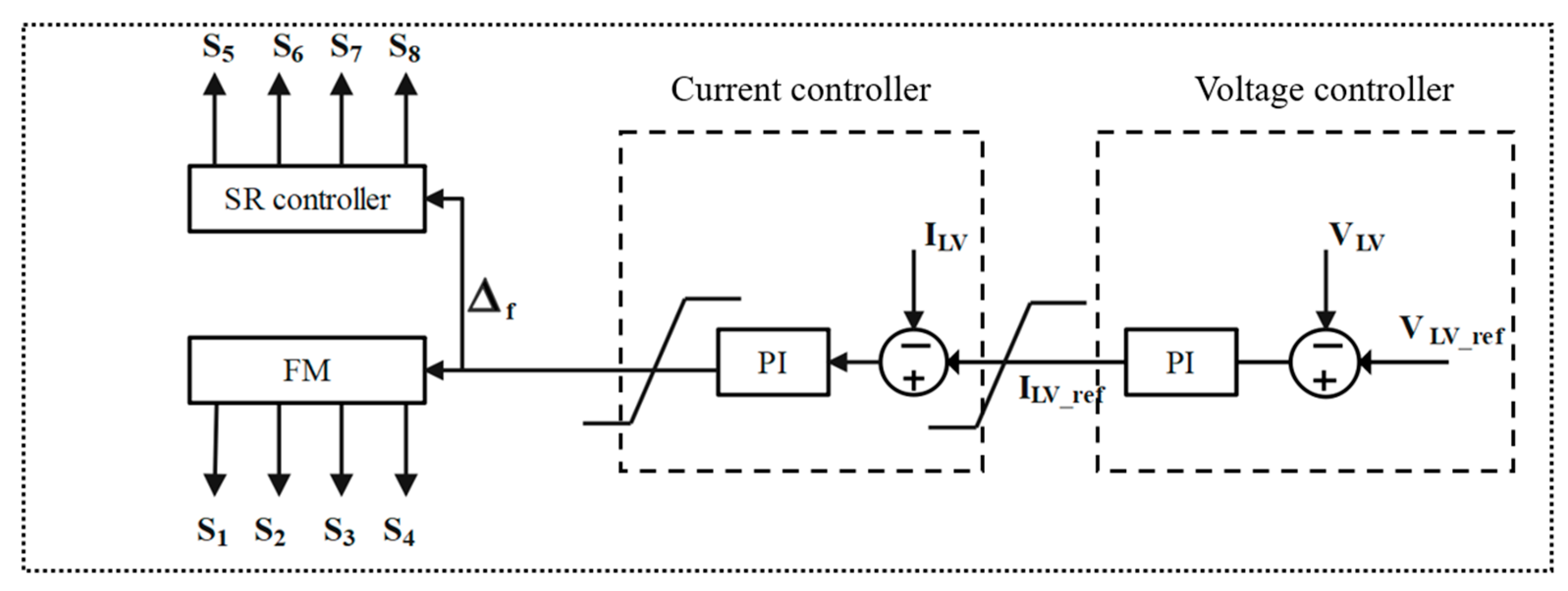
The CLLC converter is designed to achieve stable regulation of the output voltage when the electric vehicle is under a braking state. Conventional algorithms are limited by the long time they take to stabilize the output. Figure 6 depicts the control scheme with a conventional algorithm for the CLLC converter in the forward mode; the scheme includes a voltage control loop, a current control loop, and FM and SR modules.
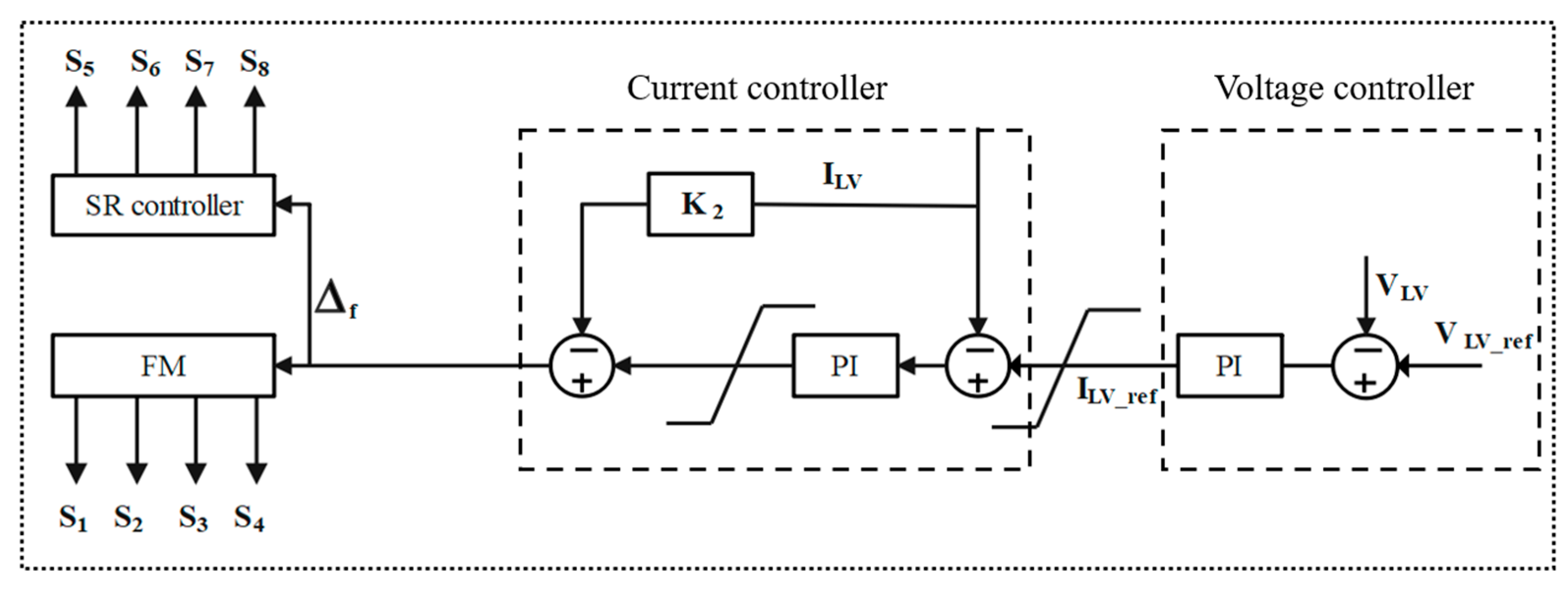
In the proposed algorithm, gain is added to the current controller to accelerate the response when the output current is higher or lower than the commanding current from PI. This is shown in Figure 7.
The difference between the conventional and the proposed algorithm is the gain compensation at the current controller. Each controller is briefly explained below.
  • Proportional–integral (PI) voltage controller: After calculating the error between the reference voltage and the output voltage on the secondary side, the PI controller calculates and exports the reference current with the gain limitation, thereby avoiding overcurrent.
  • PI current controller: After calculating the error between the reference current and the output current on the secondary side, the PI controller calculates and exports data with the gain limitation, thereby avoiding overcalculation. The exported data are compared with the value from the gain of the output current and the exported value of the deviation parameter frequency f .
  • FM module: The FM module adjusts the switching frequency of the four primary-side switches based on the value of f . These switches operate with a fixed 50% duty cycle to ensure symmetric operation and to maintain the balance of the resonant network. By modulating the switching frequency, the FM module dynamically regulates the output voltage, especially under the condition of load variation or input voltage fluctuations.
  • SR module: The SR module controls the four secondary-side switches. The SR module also responds to the value of f , but unlike the FM module, it adjusts the duty cycle of the secondary switches according to a predefined SR control algorithm. This adaptive adjustment of the secondary-side duty cycle enhances the rectification efficiency.
Figure 8 presents a simplified control block diagram of the system.
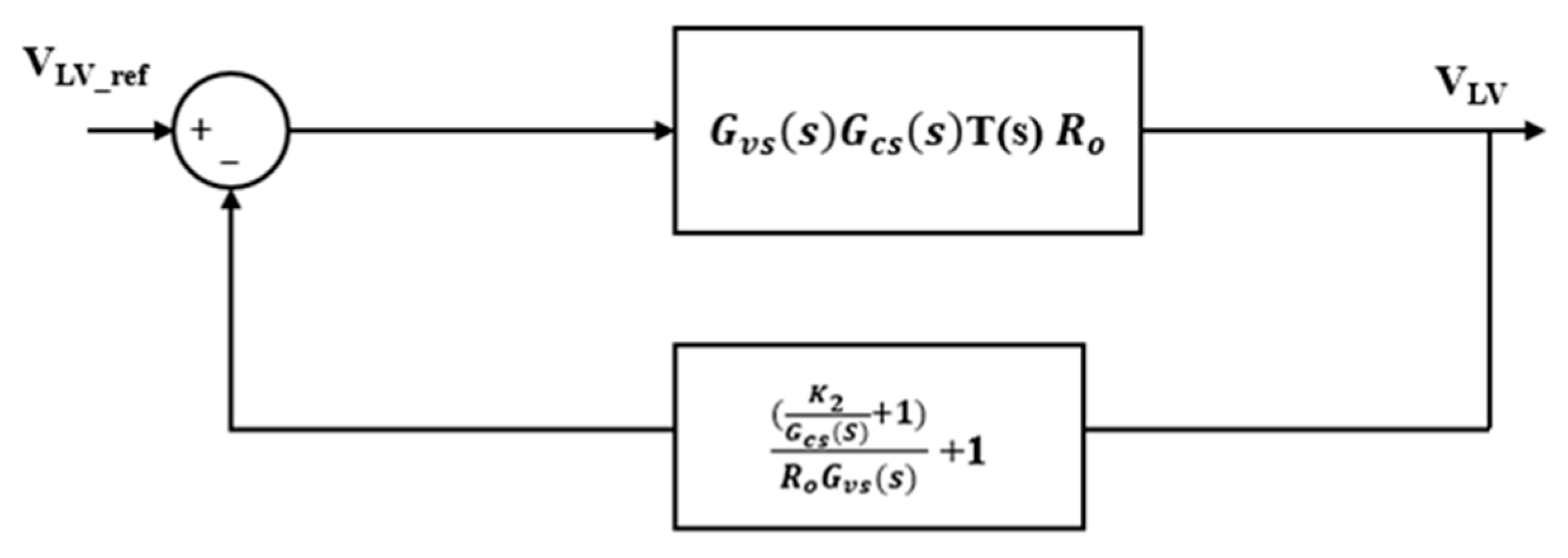
A further simplified equivalent block diagram is illustrated in Figure 9.
The root locus method is applied to design the control system [15]. To maintain the output voltage at a lower value than the maximum voltage with a safety gain of two, the overshoot is set to 20% of the output voltage, and the settling time for the output lower than 2% is set to 2 s. The design specifications are overshoot M p < 0.2 ( 20 % ) and settling time t s ( 2 % ) < 2   s . The mathematical expressions for G vs ( s ) and G cs s , the transfer functions of the voltage and current controllers, are given by Equation (34) and Equation (35), respectively.
G v s ( s ) = K p 1 + K i 1 s
G c s ( s ) = K p 2 + K i 2 s
The transfer function of the plant from Equation (33) can be expressed in terms of the zero and the pole, as follows:
T s = O 1 s 2 O 2 s 2 O 3 s 2 O 4 s 2 ( s + b ) O 5 ( s 2 ) O 6 ( s 6 )
where b = 6.045   ×   10 6 .
The closed-loop transfer function in the forward mode can be derived from Figure 9, as follows:
G s s = G v s s G c s s T s R o 1 + K 2 + G c s s + R o G v s s G c s s T s
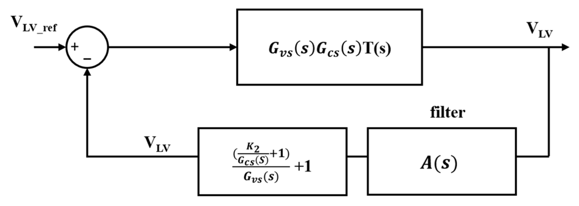
A software filter A s is added to cancel the imaginary pole of T s . The denominator of the closed-loop transfer function G s s can then be rewritten as Equation (38):
G c s = 1 + K 2 + G c s s + R o G v s s G c s s A ( s ) T ( s )
where A s = O 5 ( s 2 ) O 6 ( s 6 ) O 1 ( s 2 ) O 2 ( s 2 ) O 3 ( s 2 ) O 4 ( s 2 ) . Figure 10 illustrates the control block diagram with a filter.
The root locus equation is given in Equation (39).
1 + K 2 + G c s s + R o G v s s G c s s 1 s + b = 0
Equation (39) can be rewritten in the form of Equation (40).
1 + K p i × s + a s + c s 2 s + b
Values a, c and K p i can be determined using Equation (41).
K p i = K 2 + K p 2 + K p 1 K p 2 R o a + c = K i 2 + R o K p 1 K i 2 + R o K p 2 K i 1   K p i a × c = R o K i 1 K i 2   K p i
The damping ratio and natural frequency can be determined based on the overshoot and settling time, as shown in Equation (42).
ζ = l n 2 M p π 2 + l n 2 M p = 0.456 σ d = 4 t s = 2 = > ω d = σ d tan a r c o s ζ = 3.9   rad / sec
To design a controller that meets the transient response specifications, the dominant closed-loop system must be placed at a desired location in accordance with Equation (43).
p m = σ d + j ω d = 2 + j 3.9
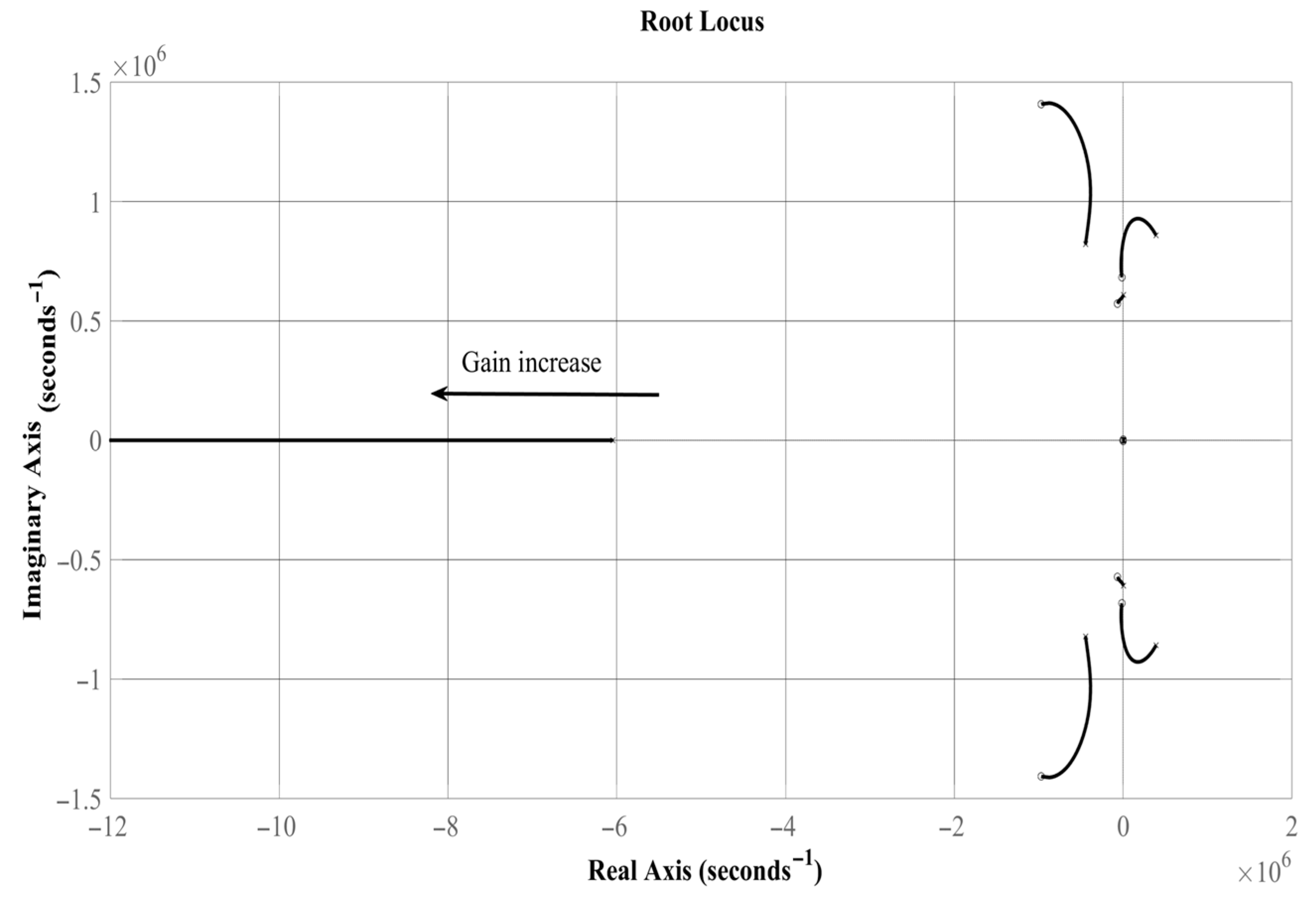
Figure 11 indicates that the root shifts to the left side when the gain increases. In the case of the desired location in Equation (43), the movement of the gain will be extremely slight, causing the root to be located near the desired location. Therefore, to achieve a substantial increase in the gain, the desired location should be chosen according to Equation (44).
p d = 1.1 × 10 6 + j 2.1 × 10 6
The zero and pole of Equation (40) are depicted in Figure 12, and the phase angle can be derived from Equation (45):
a + c b 2 1 = 180 °
where a is the phase angle of the PI zeros when s = a; c is the phase angle of the PI zeros when s = c; b is the phase angle of the plant when s = b; and 1 is the phase angle of the double zero when s = 0.
1 , c , b , and a can be determined from Equation (46).
1 = 180 ° arctan 2.1 × 10 6 1.1 × 10 6 = 117.64 ° b = arctan 2.1 × 10 6 b 1.1 × 10 6 = 23.0095 ° a + c = 2 1 + b 180 ° = 78.3015 °
If we input a = 40 ° and c = 38.3015 ° into Equation (45), the value of a and c can be determined as shown in Equation (47).
tan a = 2.1 × 10 6 a = > a = 3.6027 × 10 6 tan c = 2.1 × 10 6 c = > c =   3.7589 × 10 6
The magnitude of K p i can be calculated by using the magnitude condition at the design point p d = 1.1 × 10 6 + j 2.1 × 10 6 . The value of K p i can be determined from Equation (48).
K p i s = p d = s 2 s + b s + a s + c s = p d K p i = 8.8431 × 10 32
The values of K p 1 , K p 2 , K 2 , K i 1 , and K i 2 are determined from Equation (41), as follows:
K p 1 = 100 K p 2 = 2.037 × 10 30 K 2 = 1 × 10 32 K i 1 = 2.037 × 10 8 K i 2 = 1.131 × 10 37
Therefore, the transfer functions of the voltage and current controllers with the gain of the current controller can be determined from Equation (50).
G v s s = 100 + 2.037 × 10 8 s G c s s = 2.037 × 10 30 + 1.131 × 10 37 s K 2 = 10 32
To clarify the placement of large numerical gains such as K 2 = 1 × 10 32 and their role in the control loop, a block diagram of the digital controller implementation is shown in Figure 13. These large symbolic values arise from mathematical simplification in high-order loop-shaping equations and are not used directly in hardware. Instead, the gain K 2 and related terms are internally scaled to support a fixed-point or floating-point implementation on the STM32 microcontroller. Figure 13 illustrates how these gain terms are mapped into the digital control loop. Furthermore, saturation and quantization effects—such as those introduced by ADC resolution, PWM granularity, and signal limiting—are incorporated into the controller architecture and shown in the diagram for completeness. In practice, all signal pathways are digitally implemented using either 32-bit floating-point or scaled fixed-point arithmetic (e.g., Q15 format). Prior to implementation, symbolic gain values are numerically normalized to lie within the representable range of the microcontroller hardware. Practical limitations are also addressed in the design, including:
  • PWM resolution constraints;
  • ADC quantization affecting control accuracy;
  • Saturation handling (e.g., limiting duty cycles);
  • Rounding and small-signal sensitivity due to digital quantization.
These considerations ensure that the high-level symbolic design is translated into a realizable, numerically stable, and efficient digital controller on the target hardware.
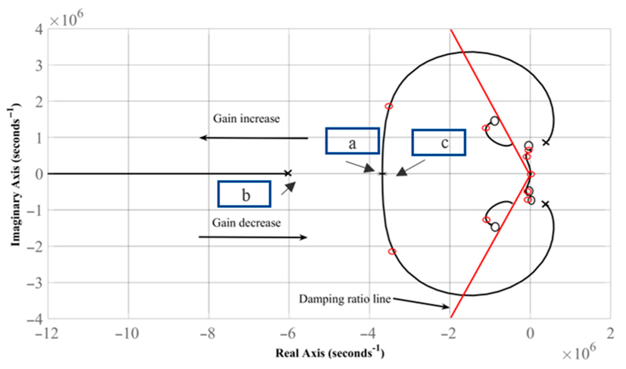
In the plot depicted in Figure 14, the damping ratio is the boundary of the design requirements, and the roots a, b, and c are near the desired location. When the gain increases, the roots will directly move to the left. Conversely, when the gain decreases, the roots directly move to the right, making the closed-loop system unstable. According to the design calculations made for the voltage and current controllers with the gain of current controllers, the roots of the closed-loop system stays on the left side, which satisfies the design requirements.
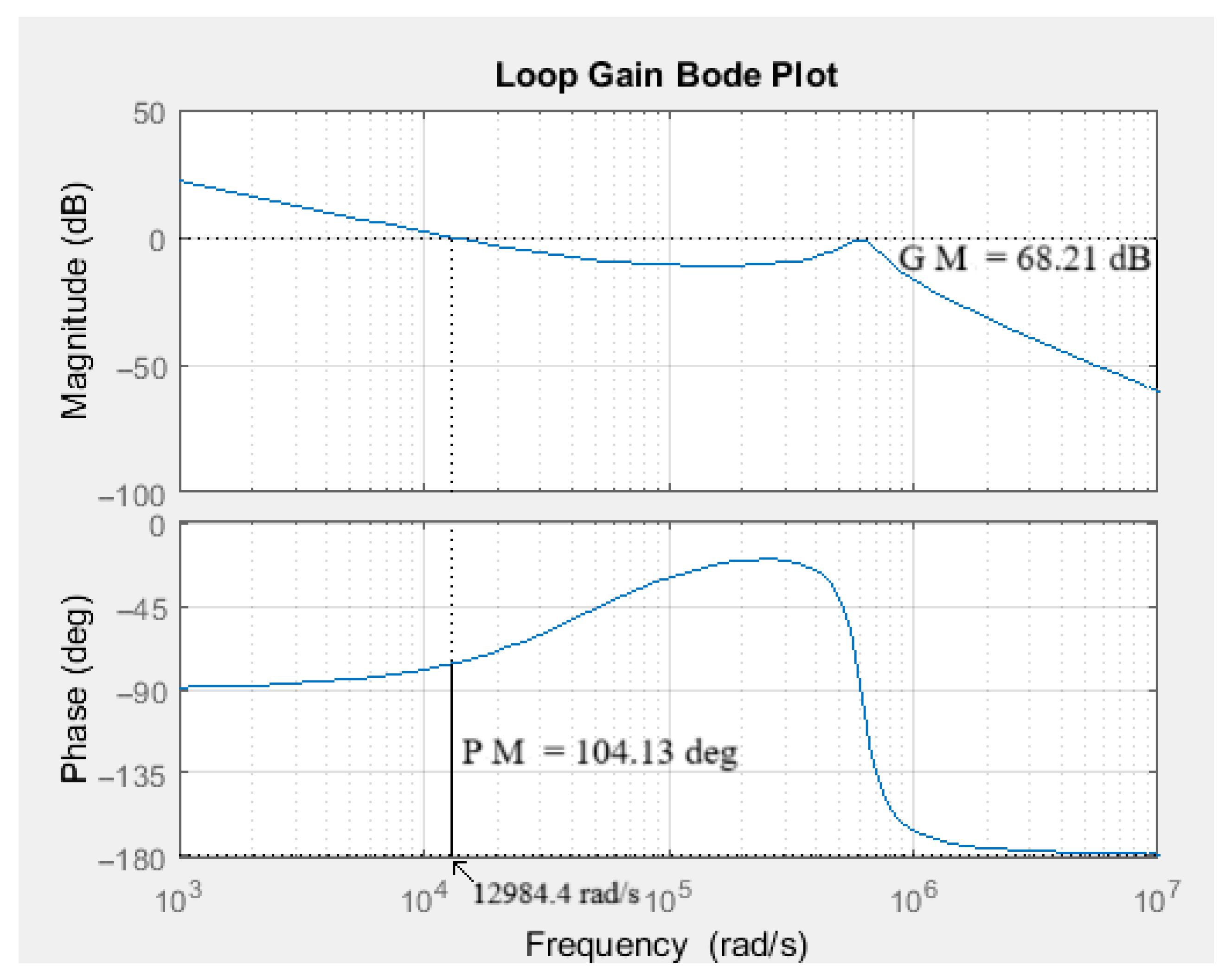
To validate the frequency domain behavior of the proposed digital controller for the bidirectional CLLC converter, the loop gain Bode plot was generated based on the small-signal transfer function derived using the First Harmonic Approximation (FHA). The resulting Bode plot is shown in Figure 15. The open-loop transfer function exhibits a gain margin (GM) of 68.21 dB and a phase margin (PM) of 104.13°, indicating a stable system with good dynamic characteristics. The crossover frequency is approximately 12,984.4 rad/s, which aligns well with the controller’s target bandwidth for electric vehicle applications. This analysis supports the time domain results and confirms that the proposed gain-compensated controller provides both stability and a sufficient phase margin, ensuring robustness under load and line variations.
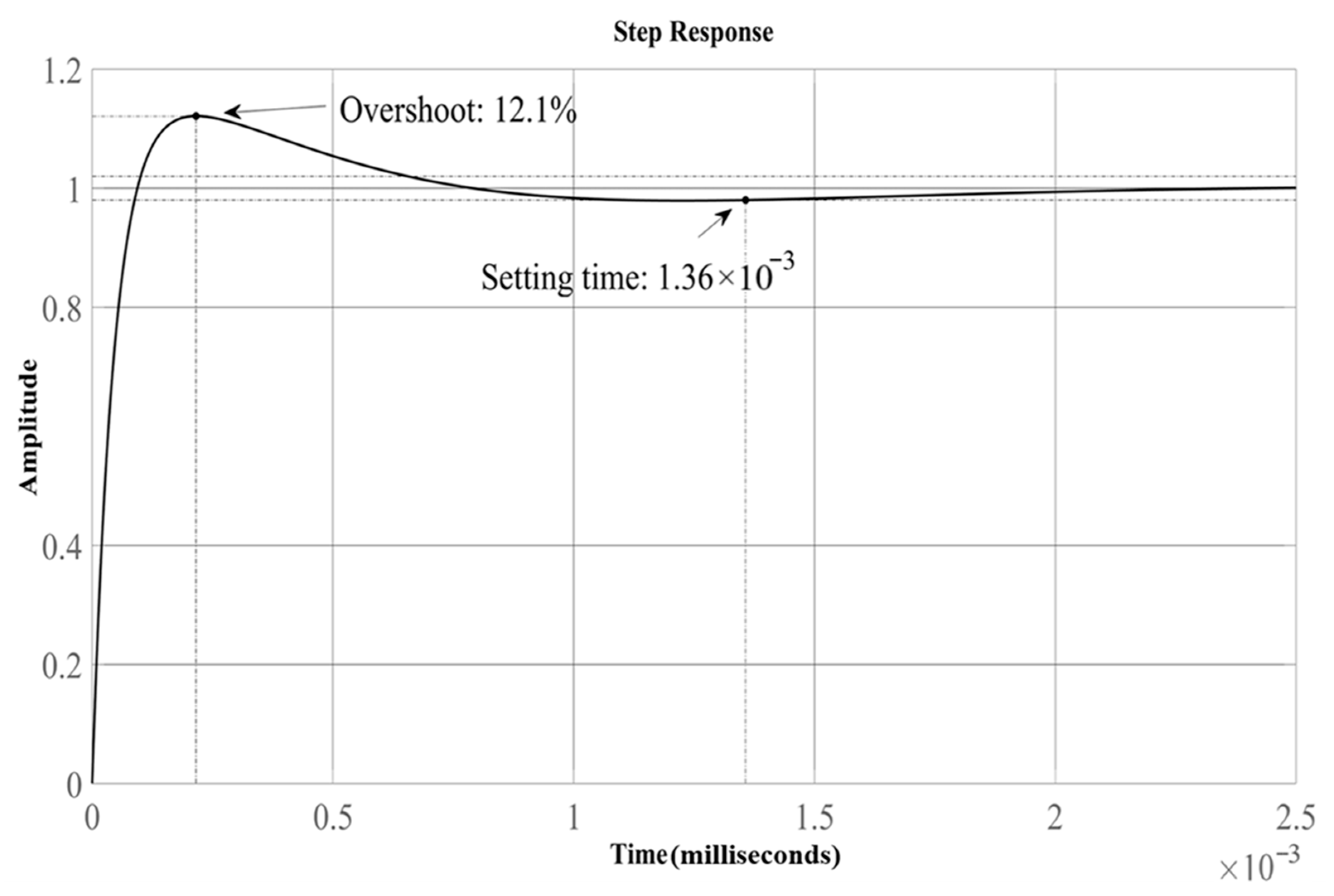
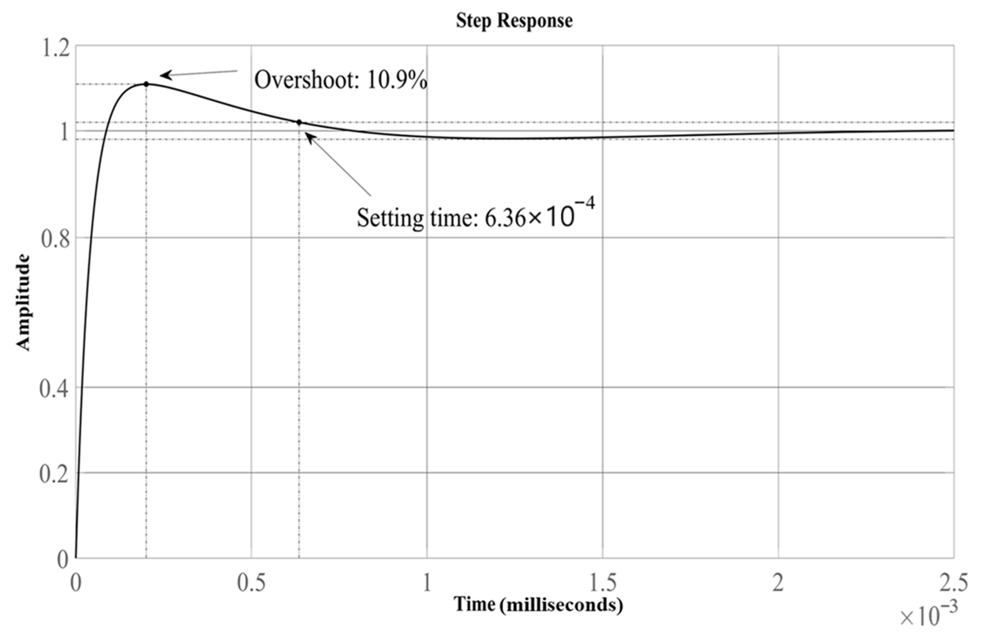
The unit-step response of the CLLC converter with the conventional algorithm features an overshoot of 12.1% and a settling time of 1.36 × 10 3 s (Figure 16), both of which satisfy the design specifications. The unit-step response of the CLLC converter with the proposed algorithm features an overshoot of 10.9% and a settling time of 6.36 × 10 3 s (Figure 17), both of which are better than the corresponding values obtained using the conventional algorithm. The control parameters of the system were determined in this section. The SR module, which increases system efficiency, will be explained and analyzed in the next section.

3.3. Synchronous Rectification (SR)

The power loss with diodes can be expressed as follows:
P l o s s = V d × I o u t
where V d is the voltage drop, and I o u t is the conducting current of the diode. The magnitude of the voltage drop typically ranges from 0.7 to 1.3 V; therefore, the SR is used for reducing the power loss in switches. The power loss with metal–oxide–semiconductor field-effect transistors is expressed as shown in Equation (52):
P l o s s = R d s × I o u t 2
where R d s is the on-state resistance, which is extremely low. Appropriate driving of the metal–oxide–semiconductor field-effect transistor when the body diode is forward-biased can improve the peak efficiency of the system by 3–4%.
The specific SR regulates the switching phase and duty cycle of the gating signals on the secondary side according to the relationship between the switching frequency f s and the first resonant frequency f r 1 . Gating signals corresponding to phase and duty cycle regulation of metal–oxide–semiconductor field-effect transistors on the secondary side under the condition f r 2 < f s < f r 1 can be expressed as shown in Equation (53):
d u t y   c y c l e = T r 1 T s × D r 1
where T r 1 is the switching period at the first resonant frequency, T r 1 = 1 f r 1 ; T s is the switching frequency period on the primary side; and D r 1 is the duty cycle of switches on the primary side.
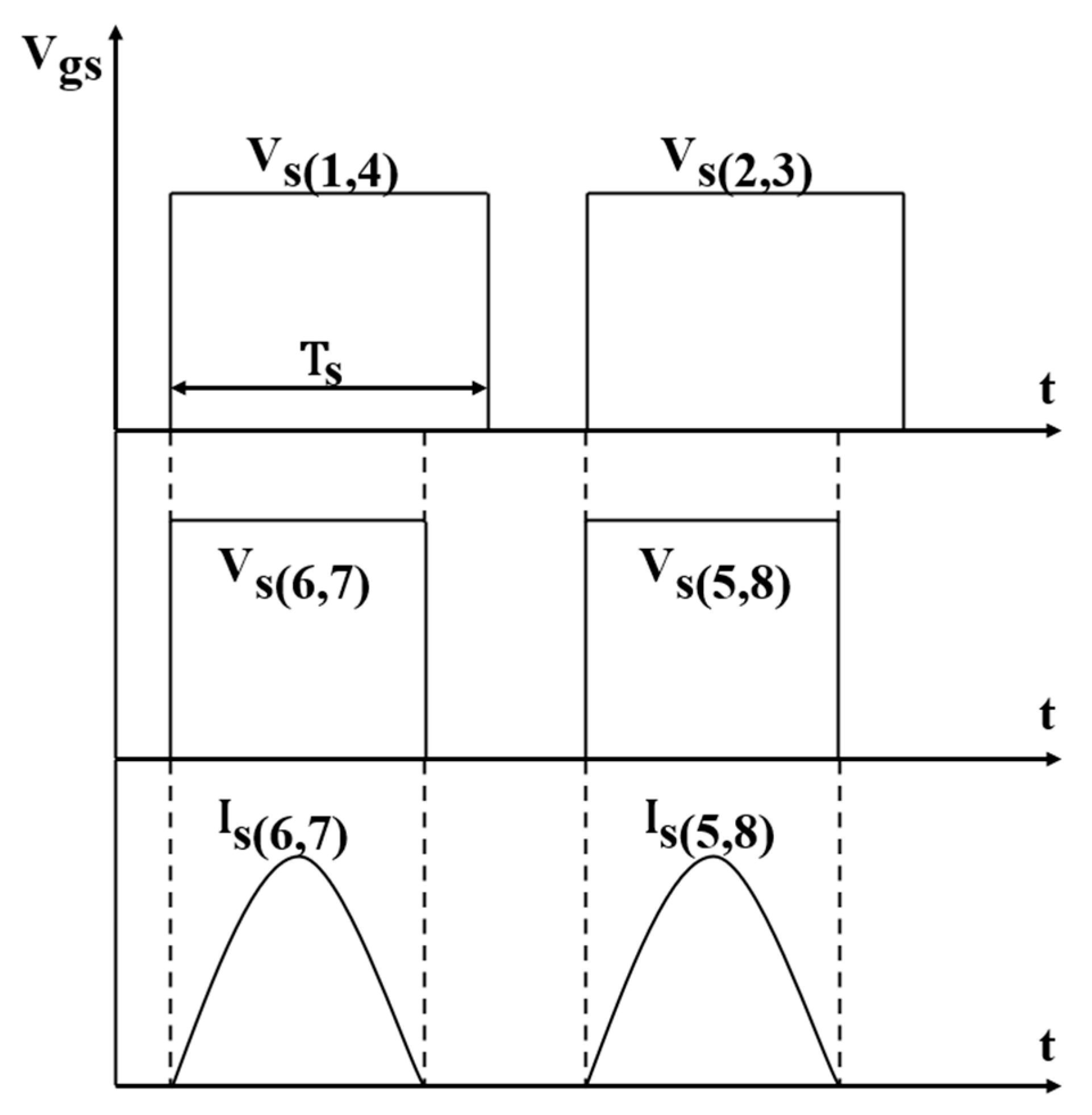
The initial phase of synchronous switching on the secondary side is consistent with that on the primary side. In the plot depicted in Figure 18, the switches S 1 and S 4 are turned on as the current flows through them, and the switches S 6 and S 7 are turned on at the same time. The mathematical expression of the duty cycle is presented in Equation (51).
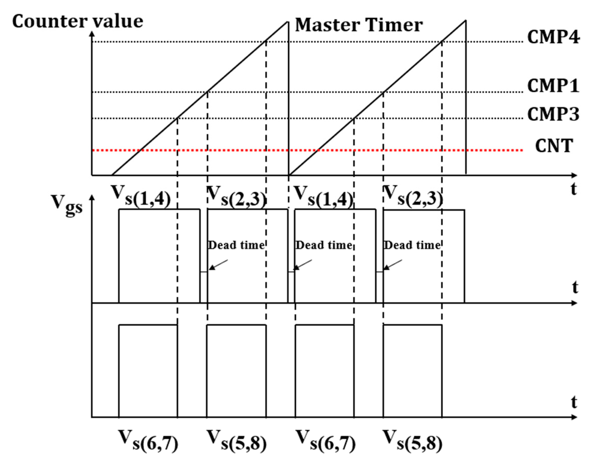
Figure 19 illustrates the control scheme of SR implemented in the microcontroller. Four timers control eight switches of the CLLC converter. The master timer deals with CMP1, CMP3, CMP4, the period, and CNT registers. The operation of the master timer involves the turning on of V s ( 1 , 4 ) and V s 6 , 7 as the CNT starts counting up. V s ( 6 , 7 ) turns off when the value of CNT exceeds that of CMP3, and V s ( 1 , 4 ) turns off when the value of CNT exceeds that of CMP1. The value of CMP1 is calculated assuming a duty cycle of 50%, and the value of CMP3 is calculated from Equation (41). By contrast, V s ( 2 , 3 ) and V s 5 , 8 turn off as the CNT reset. V s ( 5 , 8 ) turns off when the value of CNT exceeds that of CMP3, and V s ( 2 , 3 ) turns off when the value of CNT exceeds that of CMP1. In the next section, the performance of the proposed design in simulations and experiments is presented.

4. Result and Discussion

4.1. Simulation Model

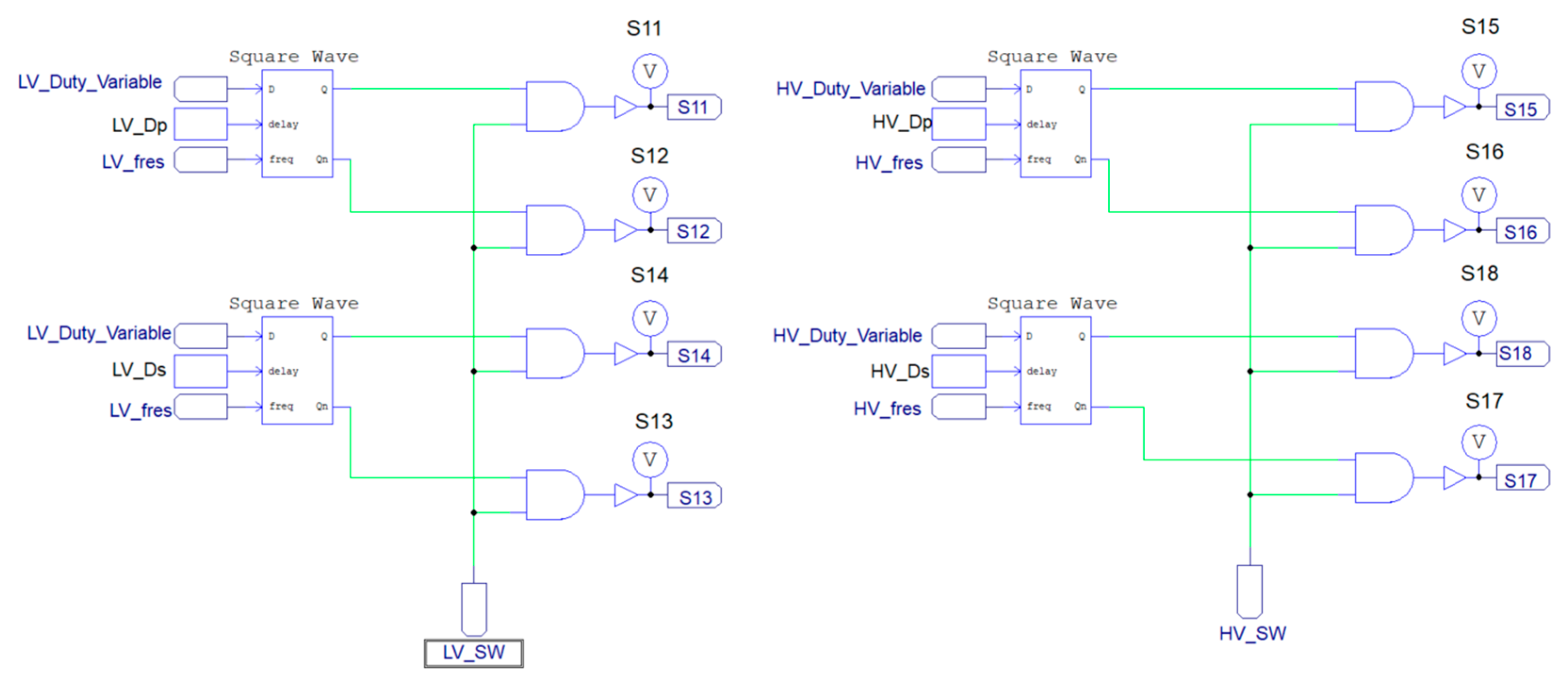
PSIM Professional 2021a.0.5 software was used to simulate the whole system, with a 400 W power rating on both the high- and low-voltage sides. The forward, reverse, and bidirectional modes were simulated using design parameters. The load in the simulation was set to a third of the maximum load. Figure 20 illustrates the model of the bidirectional CLLC resonant converter, constructed based on the theoretical analysis and component values calculated in Section 3.1 and listed in Table 2. The model incorporates all critical elements of the CLLC topology, including two resonant inductors, two resonant capacitors, a high-frequency transformer, input/output filters, and both primary and secondary full-bridge switching networks. Figure 21 presents the simulation model of the gate driver logic, which controls the switching sequences of the MOSFETs on both the high-voltage (HV) and low-voltage (LV) sides. This model generates square-wave gate signals based on frequency variables and ensures the accurate timing and dead-time insertion required for safe and efficient switching. These gate signals are then applied to the main switches to achieve the intended resonant operation and enable zero-voltage switching (ZVS) conditions.

4.2. Experimental Setup

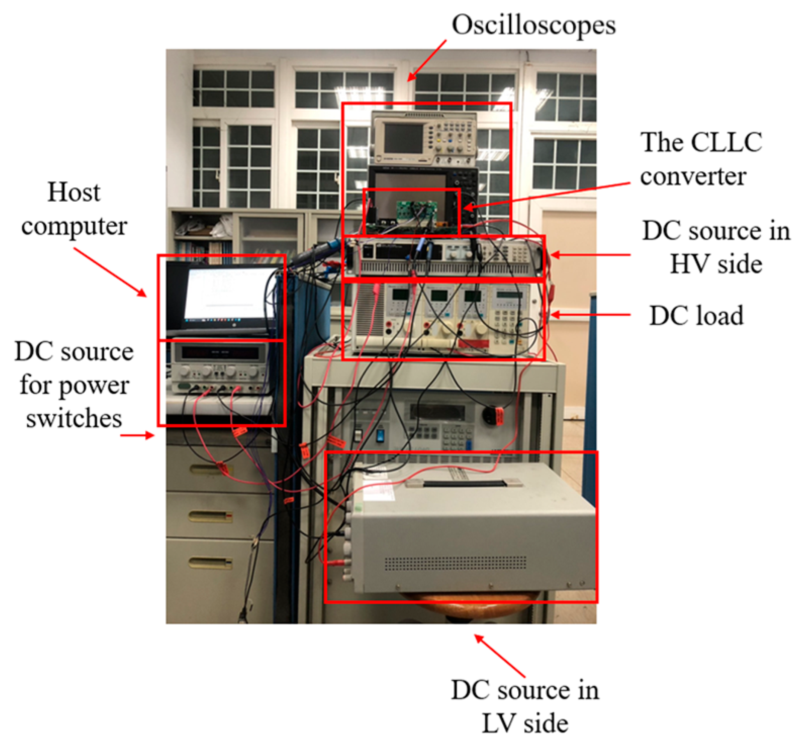
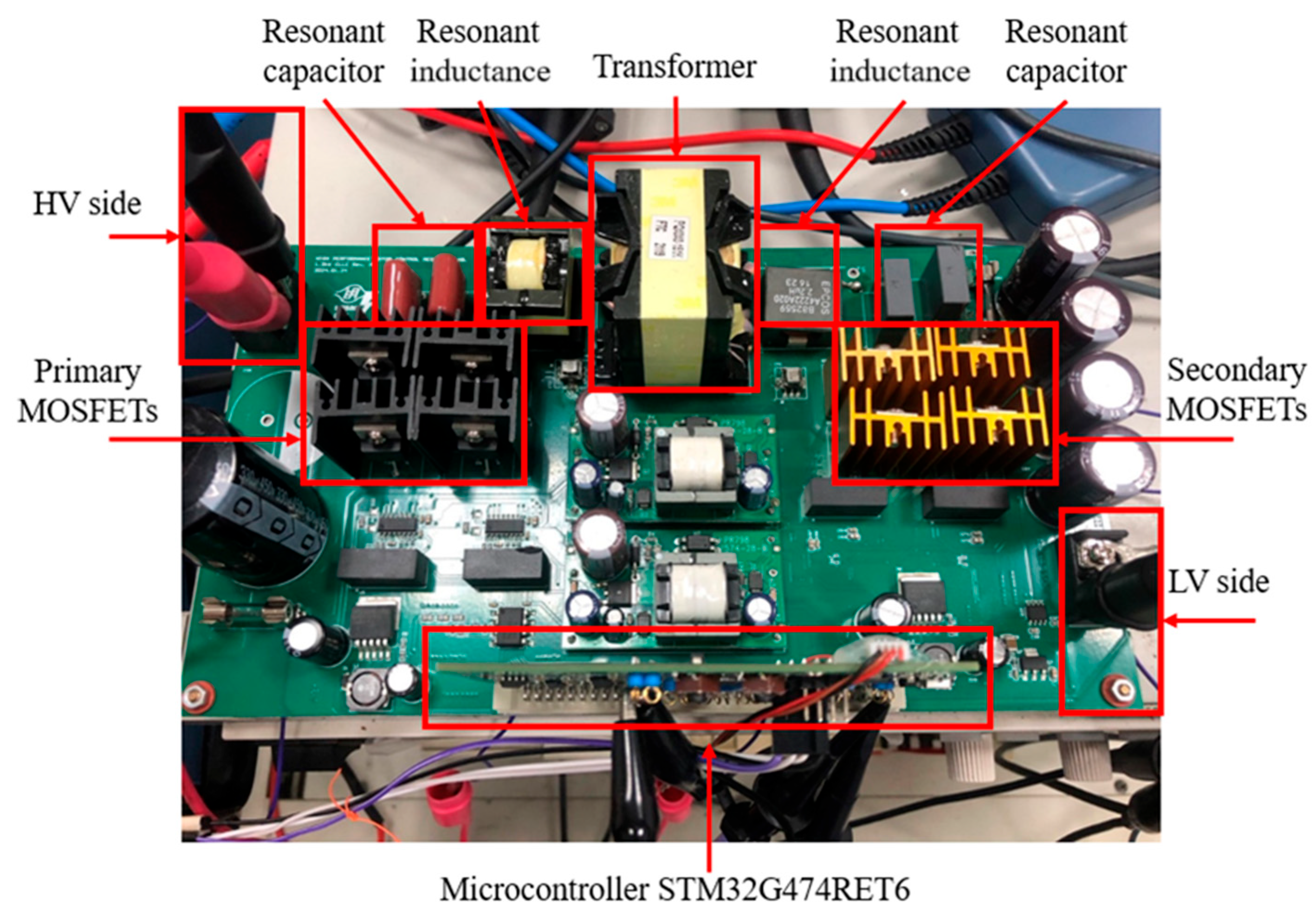
The experimental prototype of the CLLC converter was built based on the simulation model. A 32-bit microcontroller (Arm Cortex, STM32G474RET6, STMicroelectronics, Geneva, Switzerland) was used to serve as the PI voltage and PI current controller. The experimental setup is illustrated in Figure 22.
The prototype of the CLLC converter engineered in this study is displayed in Figure 23. The forward and reverse modes are operated at 400 W with a resonant frequency of 70 kHz . The CLLC converter is designed according to the specifications listed in Table 2.

4.3. Simulation and Experimental Results

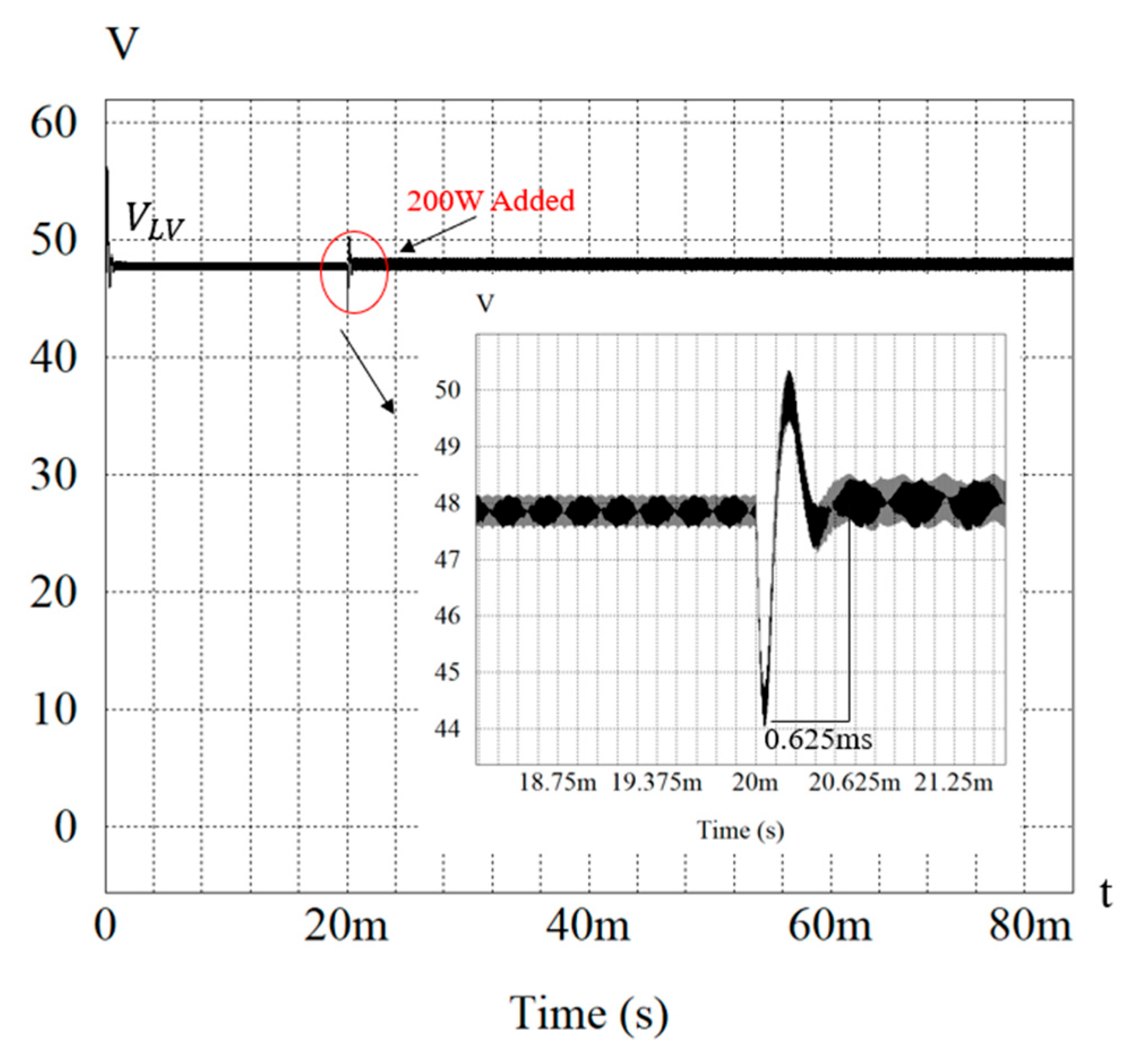
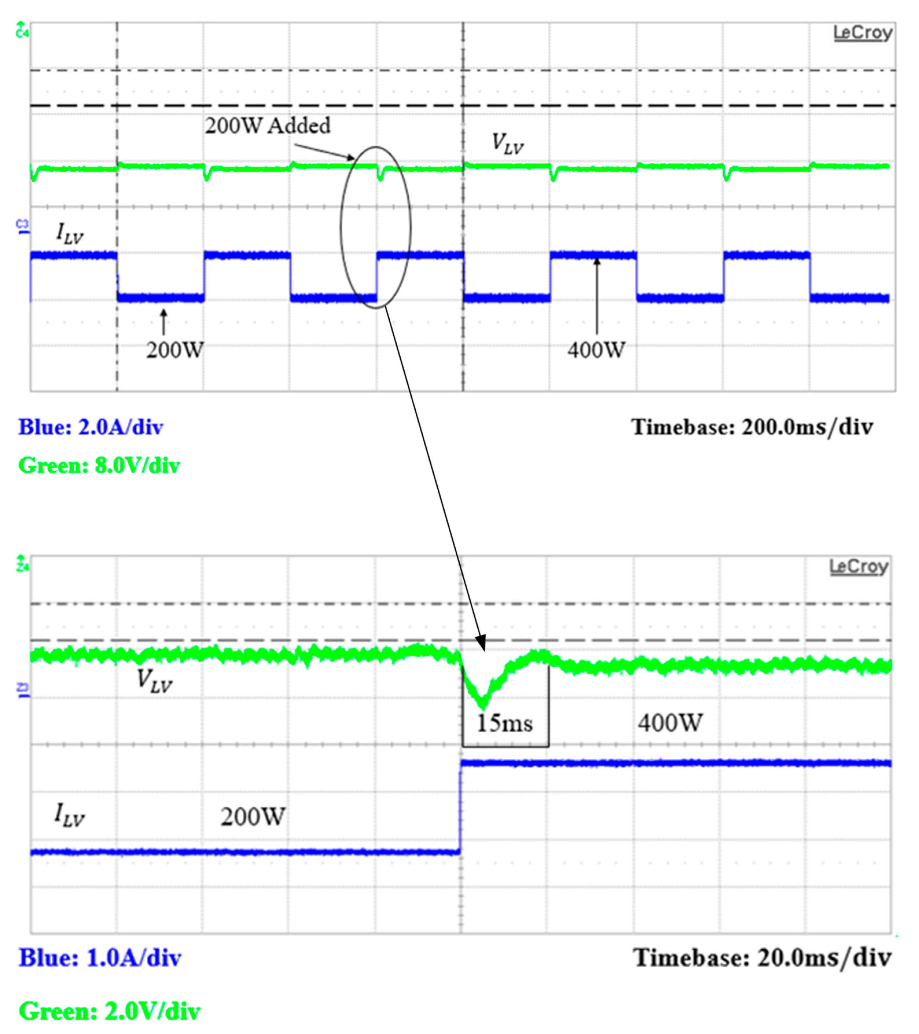
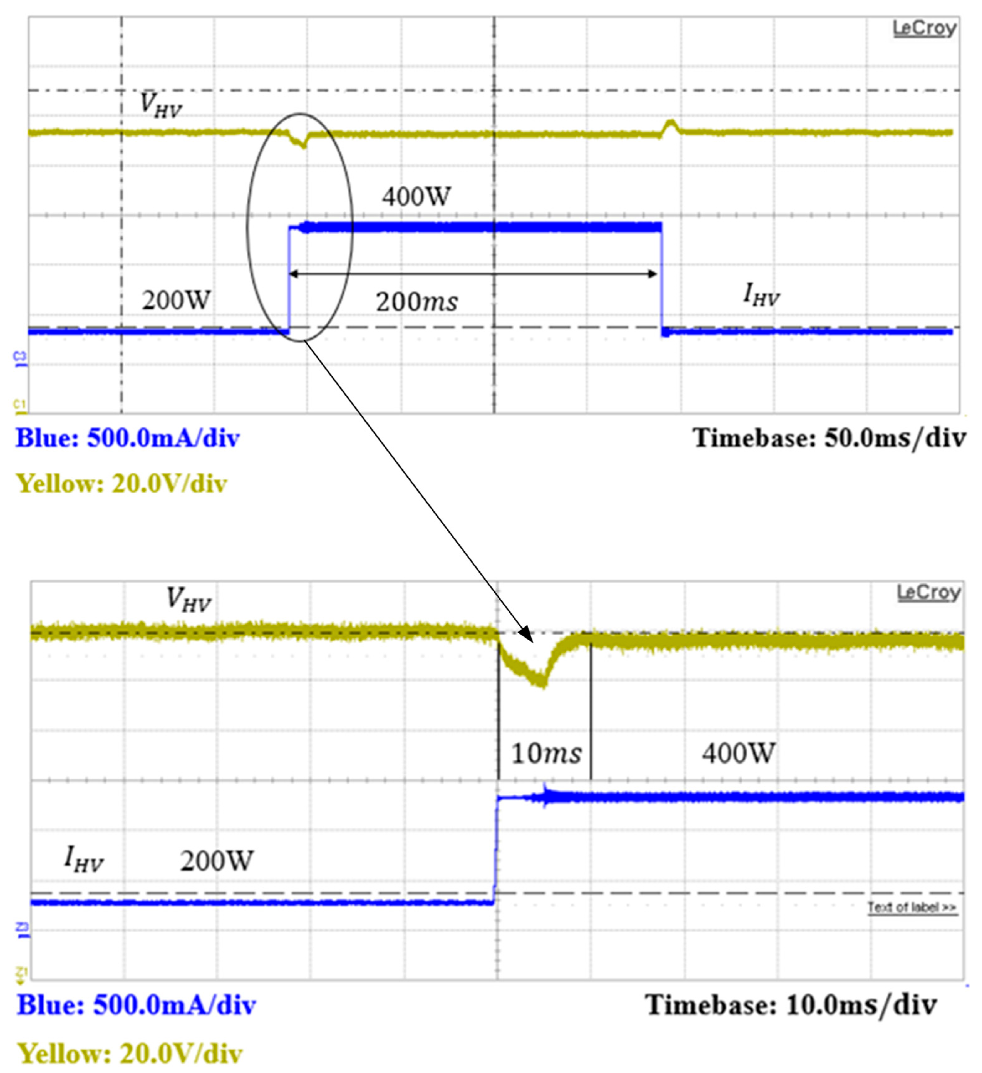
Figure 24 and Figure 25 show the simulation and experimental waveforms of output voltage at 48 V by the proposed algorithm, respectively. In a steady state, the output voltage reaches the reference voltage stably. When the load is increased from 200 W to 400 W, the output voltage drops and then returns to the reference voltage shortly. The simulation and experimental results of settling time are 0.625 ms and 15 ms, respectively. On the contrary, the voltage introduces overshot when the load is taken off, but it also returns to the reference voltage shortly. It is obvious that the settling time determined by using the proposed algorithm is shorter than that by the conventional algorithm.
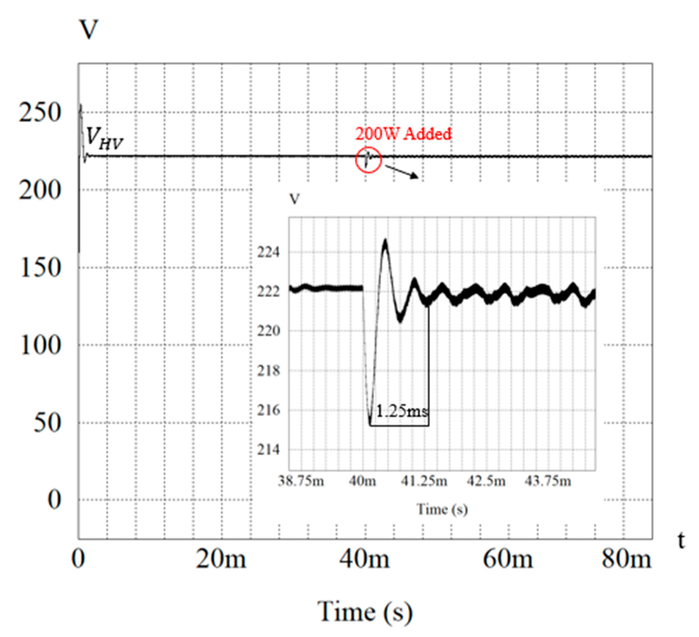
Figure 26 and Figure 27 show the simulation and experimental waveforms of output voltage at 222 V by the proposed algorithm, respectively. In steady state, the output voltage reaches the reference voltage stably. When the load is increased from 200 W to 400 W, the output voltage drops and then returns to the reference voltage shortly. The simulation and experimental results of settling time are 1.25 ms and 10 ms, respectively. It is obvious that the settling time determined by using the proposed algorithm is shorter than that by the conventional algorithm.
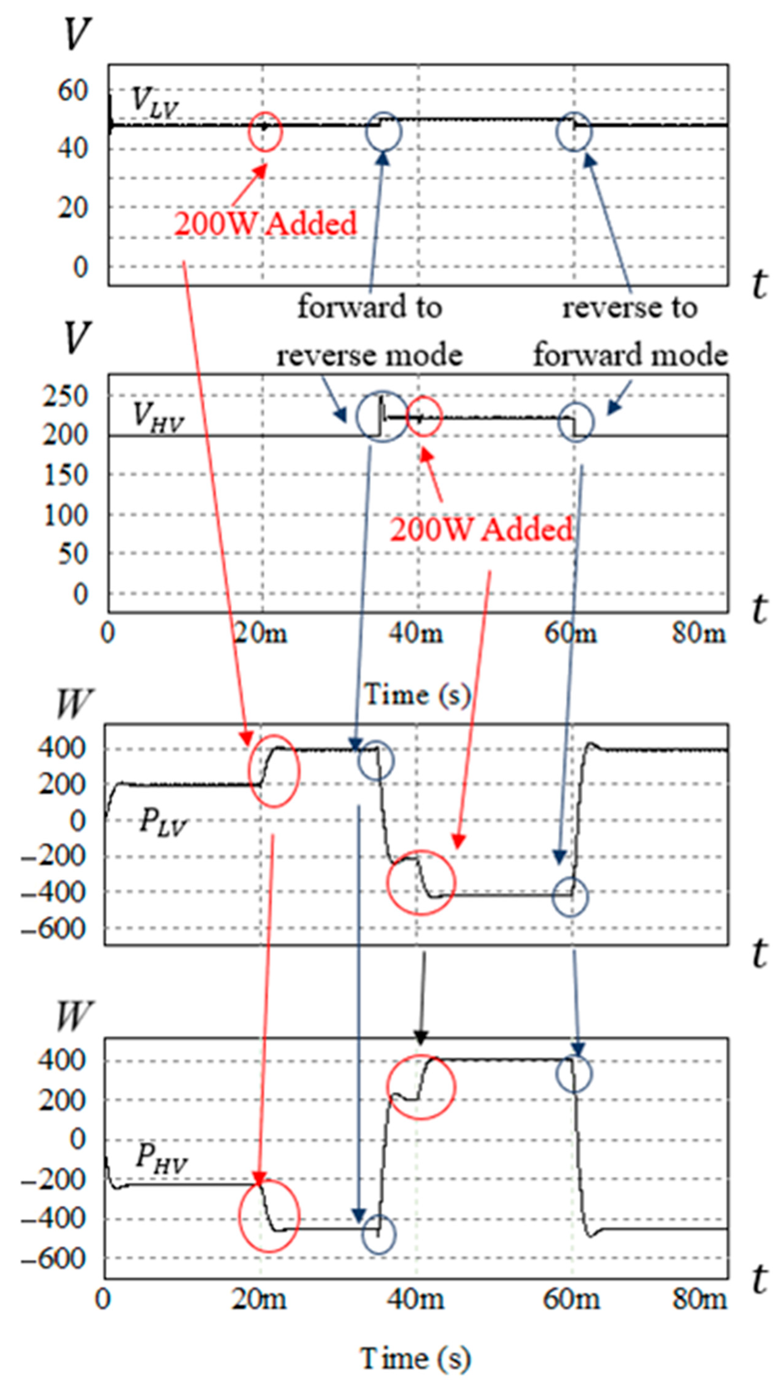
Figure 28 depicts the simulated waveforms of the mode change between the forward and reverse modes. The converter operated in the forward mode from 0 to 0.035 s and from 0.06 to 0.08 s; it operated in the reverse mode from 0.035 to 0.06 s. In the forward mode, the load increased from 200 W to 400 W at 0.02 s, and the output voltage was damp at first but returned to the steady state within a short duration. At 0.035 s, the voltage on the secondary side increased to 58 V, which was higher than the reference voltage of 48 V, prompting the converter to switch to the reverse mode. In the reverse mode, the reference voltage was 215 V, and the load was increased from 200 W to 400 W at 0.04 s. Again, the output voltage was damped at first but returned to the steady state within a short duration. The voltage on the secondary side decreased at 0.06 s, and the DC source on the primary side began to transfer power to the battery on the secondary side; therefore, the converter switched back to the forward mode and continued charging the battery on the secondary side.
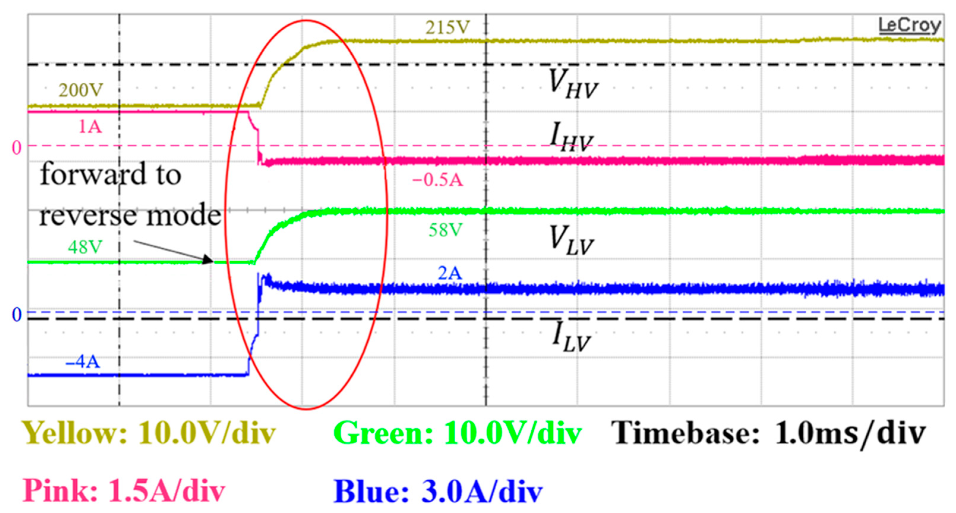
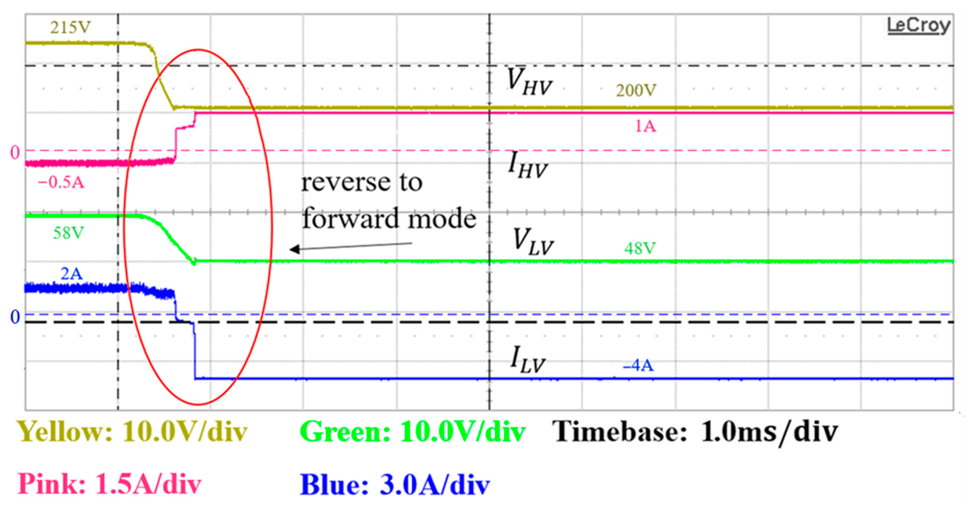
Figure 29 and Figure 30 illustrate the experimental waveforms of voltage and current in the bidirectional mode. When the output voltage on the secondary side exceeded the reference voltage of 48 V, the CLLC converter switched operations from the forward to the reverse mode. At that time point, the current on the secondary side increased, releasing power to the primary side, while the voltage on the primary side increased to the reference voltage of 215 V with a load of 100 W. Conversely, when the voltage on the secondary side was lower than or equal to the reference voltage of 48 V, the CLLC converter switched operations from the reverse to the forward mode. The primary side immediately supplied power to the secondary side, leading to an increase in the current on the primary side.
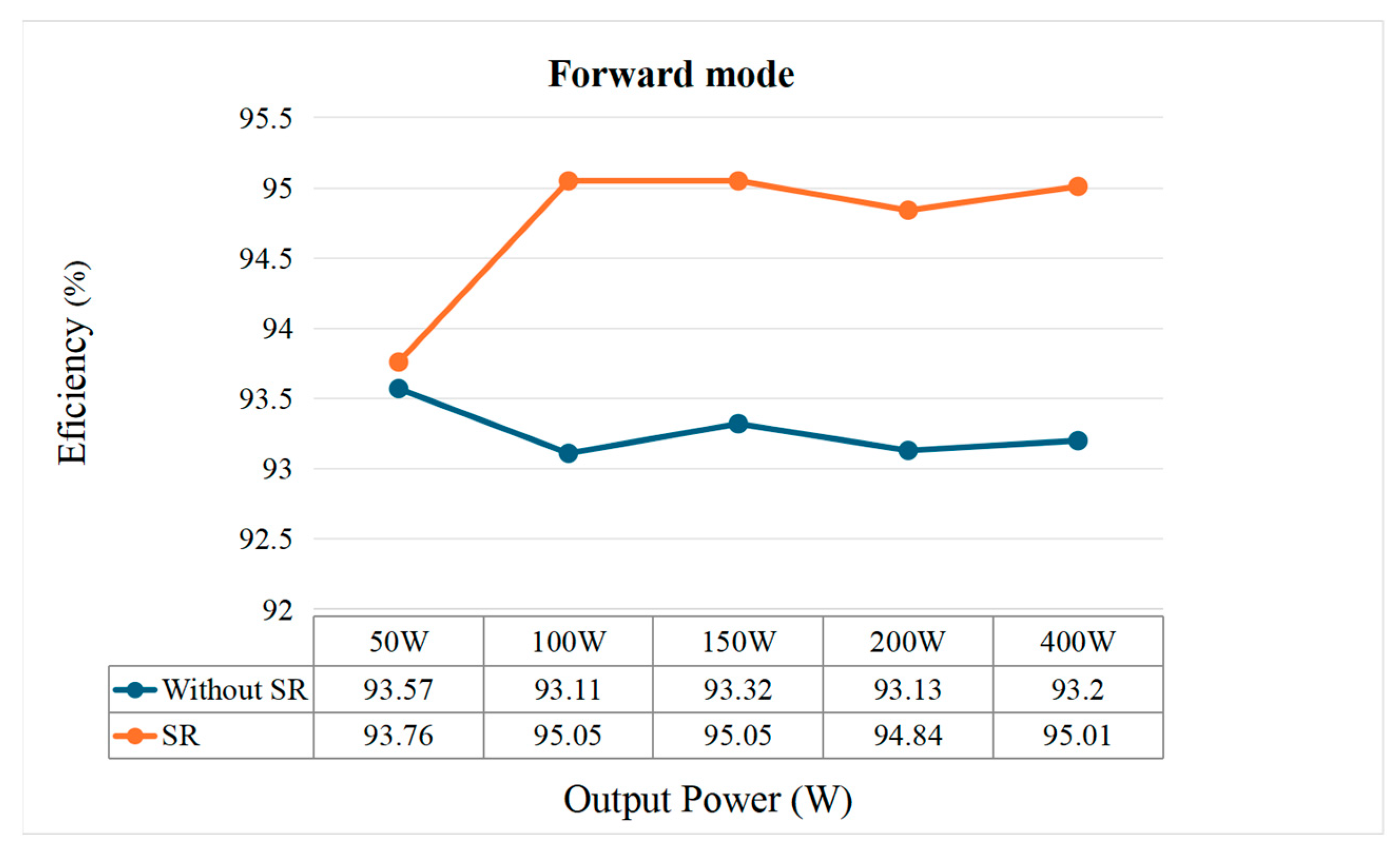
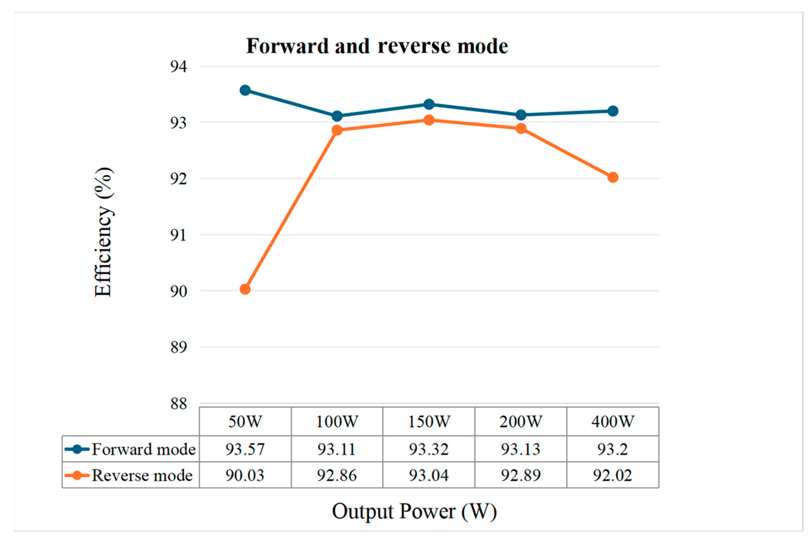
The CLLC converter operated at a power ranging from 50 W to 400 W. The conversion efficiency plots are presented in Figure 31 and Figure 32. Figure 31 depicts the conversion efficiency in the forward and reverse modes without SR. The conversion efficiency peaked at 93.57% in the forward mode and 93.04% in the reverse mode. Figure 32 depicts the conversion efficiency in the forward mode with and without SR. The efficiency was 93.11–93.57% without SR and improved to 93.76–95.05% with SR. The presence of SR significantly enhanced the conversion efficiency in the forward mode. In this implementation, the transformer’s primary side corresponds to the high-voltage side, while the secondary side operates at a lower voltage and therefore carries a higher current. In the forward mode, the resonant tank is located on the primary side, and synchronous rectification on the secondary side—where the current is higher—offers a clear efficiency benefit. However, in the reverse mode, the resonant tank shifts to the secondary side, and the high-voltage primary side carries a lower current. As a result, implementing SR provides limited efficiency gains in the reverse mode.

4.4. Discussion

The simulation and experimental results confirm that the proposed bidirectional CLLC converter achieves fast and stable dynamic responses under various operating conditions. In both forward and reverse modes, the output voltage quickly returns to its reference level following load changes, with overshoot remaining within acceptable limits. Although the experimental settling times are slightly longer than those in the simulation, the overall waveform characteristics—including voltage sag, recovery shape, and steady-state behavior—are closely aligned. The observed delays in the experimental results are attributed to non-ideal factors such as gate driver propagation delays, parasitic effects in the PCB layout, and sampling delays from the microcontroller’s ADC. Despite these real-world limitations, the results validate that the proposed gain-compensated digital control algorithm is not only effective in simulation but also robust in hardware implementation. The close agreement between simulated and measured responses supports the practical viability of the design for EV power systems. The enhanced dynamic performance of the proposed controller ensures that EV power systems can respond more rapidly to transient events such as braking or acceleration. This leads to improved voltage stability and reduced energy loss during frequent mode transitions encountered in real-world EV operations. Moreover, the use of a cost-effective STM32 microcontroller highlights the feasibility of integrating the proposed control solution into commercial on-board chargers and vehicle-to-grid (V2G) applications.

5. Conclusions

This study designed a CLLC converter that operates in the forward, reverse, and bidirectional modes. The study proposes an algorithm that reduces the settling time compared with the conventional algorithm. The optimal topology was explored, and the CLLC converter was found to be suitable for high-efficiency operations with a specific range of resonant frequencies. The operating principle of the converter was analyzed based on its topology. Moreover, the voltage gain, switching frequency, and component parameters were derived through the FHA method. Furthermore, the control block diagram was designed through small-signal analysis. The 400 W CLLC converter was simulated under the forward, reverse, and bidirectional modes of operation. In the forward mode, the proposed algorithm reduced the settling time to 0.625 ms, in contrast to 1.25 ms with a conventional algorithm; in the reverse mode, the proposed algorithm reduced the settling time to 1.25 ms, in contrast to 2.5 ms with a conventional algorithm. A 70 kHz, 400 W prototype was built with a peak conversion efficiency of 95.05% using SR in the forward mode. Without SR, the peak conversion efficiency is 93.57% in the forward mode and 93.04% in the reverse mode. In the forward mode, the proposed algorithm reduced the settling time to 15 ms, in contrast to 40 ms with the conventional algorithm; in the reverse mode, the proposed algorithm reduced the settling time to 10 ms, in contrast to 15 ms with the conventional algorithm. The settling times reported in this study are much shorter than those reported in previous studies that have employed the conventional algorithm and the same values of input voltage, L r 1 , C r 1 , L r 2 , C r 2 , L m , and output power [12].

Author Contributions

Conceptualization, M.-H.C.; Methodology, C.-D.N.; Validation, M.-H.C. and C.-D.N.; Formal Analysis, M.-H.C.; Investigation, M.-H.C. and C.-D.N.; Writing—Original Draft Preparation, C.-D.N.; Writing—Review and Editing, M.-H.C.; Supervision, M.-H.C.; Project Administration, M.-H.C. All authors have read and agreed to the published version of the manuscript.

Funding

This article was subsidized by the Ming Chi University of Technology (MCUT), Taiwan (R.O.C.).

Data Availability Statement

Data are contained within the article.

Conflicts of Interest

The authors declare no conflicts of interest.

References

  1. Gupta, R.; Rathore, A.K.; Bhatnagar, P. A Comprehensive Review of the Bidirectional Converter Topologies for the Vehicle-to-Grid System. Energies 2021, 16, 2503. [Google Scholar]
  2. Zou, S.; Lu, J.; Mallik, A.; Khaligh, A. Bi-Directional CLLC Converter With Synchronous Rectification for Plug-In Electric Vehicles. IEEE Trans. Ind. Appl. 2018, 54, 998–1005. [Google Scholar] [CrossRef]
  3. Wang, L.; Luo, W.; Huang, D. Research on Automotive Bidirectional CLLC Resonant Converters Based on High-Order Sliding Mode Control. Electronics 2022, 11, 2874. [Google Scholar] [CrossRef]
  4. Rashid, R.; Nadarajah, M.; Khan, M. Model Predictive Controller-Based CNN Controller for Optimal Frequency Tracking of Resonant Converter-Based EV Charger. Sustain. Energy Technol. Assess. 2024, 61, 103972. [Google Scholar]
  5. Lee, S.; Kim, Y.; Park, J. Research and Development Review of Power Converter Topologies and Control Strategies for EVs and Their Charging Infrastructure. Electronics 2023, 12, 1581. [Google Scholar]
  6. Zhang, F.; He, Y. Review on Classification of Resonant Converters for Electric Vehicle Fast Charging. Renew. Sustain. Energy Rev. 2021, 147, 111214. [Google Scholar]
  7. Halivor, J.; Chenguang, Y.; Ying, F. Development of Modified Sliding Mode Control of the LCC Series–Parallel Resonant Converter Based on Frequency Variation. Open Sci. J. 2023, 8, 1–17. [Google Scholar]
  8. Chen, J.-Y.; Wu, S.-Y.; Chiou, G.-J.; Juang, F.-S. Reversible Hybrid Control Resonant Converter for EV Battery Charge–Discharge System. J. Eng. 2023, 2023, e12222. [Google Scholar] [CrossRef]
  9. Chen, R.; Wu, B.; Zhou, X. A Bidirectional Half-Bridge Resonant Converter Based on Partial Power Regulation. Electronics 2024, 14, 910. [Google Scholar]
  10. EV Charging Power Topologies Design Guidebook. Available online: https://assets.wolfspeed.com/uploads/2024/01/Wolfspeed_PRD-08367_EV_Charging_Power_Topologies_Design_Guidebook_Application_Note.pdf (accessed on 7 August 2025).
  11. Shen, J.; Wang, K.; Ma, H. Quasi-Resonant Converter for Electric Vehicle Charging Applications. Energies 2024, 17, 815. [Google Scholar] [CrossRef]
  12. Yildiz, A.; de Haan, S. A Reconfigurable Two-stage 11 kW DC-DC Resonant Converter for EV Charging with a 150–1000 V Output Voltage Range. In Proceedings of the 2023 IEEE ECCE Europe, Aalborg, Denmark, 9–13 October 2023. [Google Scholar]
  13. Lu, J.; He, J. Sliding Mode Control of LLC Resonant Converters. In Proceedings of the AIEA 2023 International Conference on Photonic Energy Systems, Palm Springs, CA, USA, 21–25 February 2023. [Google Scholar] [CrossRef]
  14. Buitrago, C.S.; Cobaleda, D.B.; Martinez, W. Dual Active Bridge Converter with Variable Transformer. IEEE Access 2023, 11, 90980–90998. [Google Scholar] [CrossRef]
  15. Gu, J.; Zhang, C.; Xue, L.; Zhao, H. Comparison of Bi-Directional Topologies for On-Board Charger. Energies 2024, 17, 5496. [Google Scholar] [CrossRef]
  16. Wang, L.; Zhao, T.; Xu, J. Deep Reinforcement Learning-Aided Frequency Control of LCC-S Resonant Converters for Wireless Power Transfer Systems. arXiv 2025, arXiv:2505.01850. [Google Scholar]
  17. Tang, H.; Liu, Y.; Zhang, F. Research on Dual-Output Port On-Board Charging System Based on CLLC Resonant Converter. PLoS ONE 2023, 18, e0279558. [Google Scholar] [CrossRef]
  18. Integration of BMS Communication. Available online: https://www.monolithicpower.com/en/learning/mpscholar/battery-management-systems/bms-communication-interface/integration-of-bms-communication (accessed on 7 August 2025).
  19. Zhang, L.; He, Y. Review on Modeling and Control Strategies of DC-DC LLC Converter in Bidirectional EV Charger. Energies 2023, 16, 3946. [Google Scholar] [CrossRef]
  20. Dòria-Cerezo, A.; Boira, P.; Repecho, V.; Biel, D. Implementation of Complex-Valued Sliding Mode Controllers in Three-Phase Power Converters. arXiv 2024, arXiv:2404.03358. [Google Scholar]
Figure 1. Schematic of an electric vehicle system.
Electronics 14 03202 g001
Figure 2. Configuration of the CLLC converter.
Electronics 14 03202 g002
Figure 3. Operating states of the CLLC converter: (a) State 1 [t0t1]; (b) State 2 [t1t2]; (c) State 3 [t2t3]; (d) State 4 [t3t4]; (e) State 5 [t4t5]; and (f) State 6 [t5t6].
Electronics 14 03202 g003
Figure 4. Theoretical waveforms of the CLLC converter.
Electronics 14 03202 g004
Figure 5. Equivalent circuit of the CLLC converter in the forward mode obtained through the FHA method.
Electronics 14 03202 g005
Figure 6. Control scheme with conventional algorithm in the forward mode.
Electronics 14 03202 g006
Figure 7. Control scheme with proposed algorithm in the forward mode.
Electronics 14 03202 g007
Figure 8. Control diagram of the proposed algorithm in the forward mode.
Electronics 14 03202 g008
Figure 9. Equivalent block diagram.
Electronics 14 03202 g009
Figure 10. Block diagram with a filter.
Electronics 14 03202 g010
Figure 11. Zero and pole of the plant.
Electronics 14 03202 g011
Figure 12. Zero and pole of the calculated closed-loop system on the S-plane.
Electronics 14 03202 g012
Figure 13. Block diagram of the digital control system showing the gain locations and numerical scaling.
Electronics 14 03202 g013
Figure 14. Root locus of the proposed algorithm.
Electronics 14 03202 g014
Figure 15. Loop gain Bode plot for the control-to-output transfer function.
Electronics 14 03202 g015
Figure 16. Unit-step response with the conventional algorithm.
Electronics 14 03202 g016
Figure 17. Unit-step response with the proposed algorithm.
Electronics 14 03202 g017
Figure 18. Gating signal of switches for f r 2 < f s < f r 1 .
Electronics 14 03202 g018
Figure 19. Control scheme of SR with microcontroller.
Electronics 14 03202 g019
Figure 20. Simulation model of the CLLC converter.
Electronics 14 03202 g020
Figure 21. Simulation model of the gate driver logic.
Electronics 14 03202 g021
Figure 22. Experimental prototype of the CLLC converter.
Electronics 14 03202 g022
Figure 23. CLLC converter.
Electronics 14 03202 g023
Figure 24. The simulation result of output voltage in the proposed algorithm at forward mode.
Electronics 14 03202 g024
Figure 25. The experimental result of output voltage in the proposed algorithm at forward mode.
Electronics 14 03202 g025
Figure 26. The simulation result of output voltage in the proposed algorithm at reverse mode.
Electronics 14 03202 g026
Figure 27. The experimental result of output voltage in the proposed algorithm at reverse mode.
Electronics 14 03202 g027
Figure 28. Simulated waveforms of input/output voltage and power in the bidirectional mode.
Electronics 14 03202 g028
Figure 29. Experimental waveforms of input/output voltage and current from the forward to the reverse mode.
Electronics 14 03202 g029
Figure 30. Experimental waveforms of input/output voltage and current from the reverse to the forward mode.
Electronics 14 03202 g030
Figure 31. Conversion efficiency in the forward and reverse modes without SR.
Electronics 14 03202 g031
Figure 32. Conversion efficiency in the forward mode with and without SR.
Electronics 14 03202 g032
Table 1. Comparison of control strategies for bidirectional CLLC resonant converters.
Control StrategySpeed (Settling Time)Robustness to Load/Line VariationsImplementation ComplexityRemarks
Proposed Gain-Compensated PI (This work)10–15 msModerate to HighLowSimple to implement on microcontroller; efficient for EV applications
Model Predictive Control (e.g., [3])~5 msHighHighRequires full system modeling and computationally intensive optimization
AI-Based Control (e.g., [4,14])~4–6 msHighVery HighDemands large training datasets and additional hardware resources
Hybrid Control (e.g., [6,11])~6–10 msHighMediumComplex design but offers good trade-off in performance
Table 2. Specifications of the CLLC converter.
The CLLC Converter Parameters
HV side V H V _ m i n = 100   V
V H V _ n o m = 200   V
V H V _ m a x = 220   V
LV side V L V _ m i n = 45   V
V L V _ n o m = 48   V
V L V _ m a x = 60   V
Output power P o = 400   W
Resonant frequency f r = 70   kHz
Switches frequency f s _ m i n = 40   kHz
f s _ m a x = 95   kHz
Disclaimer/Publisher’s Note: The statements, opinions and data contained in all publications are solely those of the individual author(s) and contributor(s) and not of MDPI and/or the editor(s). MDPI and/or the editor(s) disclaim responsibility for any injury to people or property resulting from any ideas, methods, instructions or products referred to in the content.