Abstract
Low-frequency (LF) time code timing technology holds significant importance in civilian applications such as radio-controlled clocks. This study focuses on the design and implementation of a high-precision Binary Phase Code (BPC) LF time code signal generator. A generator system was constructed, demonstrating good stability, superior resolution, and flexible adjustment capabilities for both amplitude and phase. The system employs an ARM + FPGA cooperative architecture: the ARM processor is responsible for parsing and scheduling the time code data, while the FPGA implements carrier wave generation and high-precision digital modulation. This digital processing is combined with analog circuitry to achieve digital-to-analog (D/A) signal conversion. Compared to traditional methods, carrier generation is achieved using Direct Digital Synthesis (DDS) technology. Digital modulation techniques enable the precise control of the modulation depth (adjustable between 70% and 90%) and phase (with a resolution of 1 ns). A sliding window algorithm was utilized for time difference calculation and compensation. Testing confirmed the stability of key signal parameters, including integrity, carrier frequency and modulation depth. These results validate the feasibility and superiority of the digital LF time code generation technology proposed in this study, providing a valuable reference for the development of next-generation timing equipment.
1. Introduction
Low-frequency (LF) time code signals are encoded signals transmitted within the low-frequency range (30 kHz–300 kHz) that carry standard time, date, and related information [1]. BPC LF time code timing technology offers several advantages. From the perspective of signal propagation characteristics, LF signals exhibit superior long-distance transmission capabilities and strong penetration (covering scenarios such as indoor and underground environments). This is due to the favorable reflection properties of LF band electromagnetic waves by the Earth’s surface and the ionosphere. Consequently, LF signals overcome the line-of-sight (LOS) propagation limitations inherent to higher-frequency signals. An LF time code transmission station can cover a radius of 1000 to 3000 km, making it highly suitable for wide-area timing requirements [1,2,3]. Regarding cost, common LF time code system receiving terminals, such as radio-controlled clocks and dedicated receiver modules, are inexpensive. This cost-effectiveness facilitates large-scale popularization. Therefore, LF time code timing technology plays a significant role in civilian timekeeping, power grid management, transportation systems, financial operations, and other fields. It holds particular and irreplaceable importance in the domain of radio-controlled timepieces. Table 1 shows a comparison between low-frequency time code timing technology and other timing technologies.

Table 1.
Comparison between low-frequency (LF) time code timing technology and other timing technologies [4,5,6,7,8,9].
Since the 1950s, with the continuous improvement in atomic clock accuracy and rapid advancements in microelectronics technology, low-frequency time code timing technology has garnered widespread international attention and application. Countries including Germany, the United States, and Japan have successively established LF time code transmission systems. The geographical distribution of global LF time code timing systems is illustrated in Figure 1.
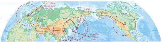
Figure 1.
Global geographical distribution of operational low-frequency (LF) time code timing systems.
According to documented information, the encoding schemes and signal formats adopted for low-frequency (LF) time code systems vary significantly across different nations [10]. The technical parameters of globally major LF timing stations are comparatively presented in Table 2.
Table 2.
Comparative analysis of technical parameters for major low-frequency (LF) time code timing stations.
The frame lengths of low-frequency time code transmitting stations abroad are generally long. Most of them still use AM, with relatively long frame lengths (about 60 s), and lack effective error correction methods. This article is based on the BPC encoding system, compressing the frame length to 20 s, which is conducive to rapid clock adjustment, and the BPC signal adopts the amplitude modulation technology of pulse width, making reception and demodulation more convenient.
China’s low-frequency time code transmission station was commissioned in 2007, emitting BPC-format signals at 68.5 kHz with 100 kW transmitter power. Research advancements in BPC signal processing include Bai Yan et al.’s development of high-precision receiver timing techniques. Their numerical approach utilizes spline interpolation and least squares fitting to identify second-pulse reference markers, elevating BPC receiver timing accuracy to the tens-of-microseconds range [11]. Luo Xinyu et al. incorporated a weighted algorithm for BPC signal reception, proposing a detection method that integrates signal average power and carrier power metrics [12]. This innovation effectively resolves interference detection challenges in LF time code systems while enhancing robustness against high-power jamming sources. Further extending the theoretical frontier, however, these studies mainly focus on enhancing accuracy at the receiving end, with few studies conducted at the transmitting end. In this paper, the accuracy at the transmitting end is improved by enhancing the control mode and introducing the sliding window algorithm, which makes up for the deficiency of the transmitting end’s accuracy.
Feng Ping, Huang Luxi and others have studied the system and timing system of BPC signals. These studies have focused on and investigated the coding method, carrier, modulation method, signal evaluation and other aspects of BPC low-frequency time code timing signals [13]. Based on these studies, this paper determines the optimal transmission and modulation methods for BPC signals and then conducts complete hardware implementation based on digital means. This research can be used as a platform to conduct more convenient experimental verification of the theory.
Current research indicates that the transmitter of BPC low-frequency time code signals significantly impacts the signal quality and timing precision of the entire LF timing system. Deviations in key transmitter parameters—including carrier frequency, modulation depth, and phase—become amplified during propagation via skywave and groundwave paths. This directly compromises receiver-side performance metrics, ultimately degrading overall signal integrity and timing accuracy. Consequently, a highly stable and fine-resolution BPC LF signal generator is essential for transmission systems.
This paper presents an ARM-FPGA-based LF time code generator with adjustable phase and amplitude. Laboratory testing demonstrates its exceptional stability in maintaining carrier frequency, phase jitter, and modulation depth while successfully synchronizing radio-controlled clocks under controlled conditions. The design employs Direct Digital Synthesis (DDS) technology combined with phase-locked loops to generate 68.5 kHz carrier signals. Compared to legacy equipment relying on 68.5 kHz crystal oscillators, this approach achieves superior frequency accuracy. Additionally, the output signal’s adjustable amplitude and programmable phase provide greater adaptability and operational flexibility across diverse scenarios, substantially enhancing practical utility.
2. Module Design for BPC Low-Frequency Time Code Signal Generator
2.1. Time Code Generation Module Design
The BPC low-frequency time code generator system accepts inputs of a standard time source signal along with a precise 1PPS (Pulse Per Second) signal and frequency reference. It outputs a modulated BPC signal at 68.5 kHz. The generation process is illustrated in Figure 2.
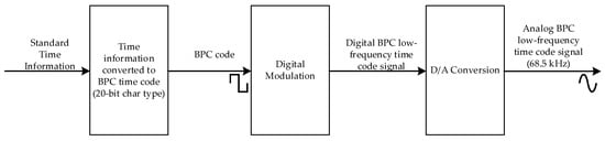
Figure 2.
BPC low-frequency time code signal generation process.
The standard time source is typically an external atomic clock or another high-precision time reference, generally provided in the Time of Day (TOD) message format. The structure of a received TOD message is assumed to follow the specifications shown in Table 3.
Table 3.
TOD message and explanation.
To distinguish TOD time-encoded information from interference at the serial input port, we require a processor chip with serial port functionality and multi-threading capability to construct the time code generation module and design peripheral analog circuits. Consequently, we implemented the time code generation module using an ARM architecture chip [14,15].
The STM32F107 chip, an ARM-based microcontroller from STMicroelectronics, features six UART/USART serial ports capable of receiving external standard time information and control commands via serial communication. With its wide operating temperature range, excellent electromagnetic compatibility, and cost-effectiveness, this device operates at 2.0 V to 3.6 V supply voltage and incorporates a 72 MHz Cortex-M3 core—specifications fully adequate for BPC time code generation and control tasks.
The time encoding generation module based on ARM design has two Usart serial ports. One Usart serial port can receive standard TOD time information from an external time source or an upper computer, update the local time (Localtime), and convert Localtime into 20 char-type BPCs according to the BPC encoding format. Another Usart serial port sends different information to the outside (for details, see the relevant content in Section 2.1). In addition, the ARM chip also has a set of 8-bit address/data multiplexing lines and three control lines to communicate with the signal generation module. Table 4 presents the updated LocalTime information based on the data shown in Table 3 [13,16].
Table 4.
Updated LocalTime information.
2.2. Signal Generation Module Design
The generated BPCs are transmitted to the signal generation module, where they are digitally synthesized with a 68.5 kHz carrier signal to produce the digital-format BPC time code. A complete BPC signal frame has a duration of 20 s. As shown in Figure 3, the beginning time segment τ of each integer second contains a negative pulse signal with an amplitude lower than that of the nominal carrier signal. The negative pulse amplitude is adjustable, typically set to 10–30% of the standard carrier amplitude. The pulse duration varies between 100 ms, 200 ms, 300 ms, and 400 ms intervals. The waveform schematic of the low-frequency time code signal is illustrated in Figure 3.
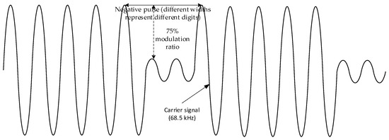
Figure 3.
BPC low-frequency time code signal waveform diagram.
The duration of the negative pulse at the beginning of each integer second corresponds to its represented meanings as seen in Table 5.
Table 5.
The duration of negative pulses and their corresponding meanings.
Next, I will derive the time-domain and frequency-domain expressions of a frame of a BPC low-frequency time code signal and draw its spectrogram. By doing so, the frequency-domain measurement result images in Section 4.2 can be directly compared with this image to verify the correctness of this design.
If τ = 1, it indicates the current second is the frame start second. The baseband signal within a complete 1 s BPC signal can be expressed as follows:
where k is the modulation index (the ratio of negative pulse amplitude to nominal signal amplitude), and represents a rectangular function with width and amplitude k:
When τ takes the value , the signal for that second can be expressed as follows:
Performing Fourier transform on Equation (3) yields its frequency-domain representation as follows:
Here, the definition of the function sa () is as follows: .
However, in practical scenarios, perfect rising/falling edges do not exist. Assuming actual edges exhibit smooth slopes with duration Δ, the negative pulse within each second transforms into a trapezoidal signal with high-level edges of duration , as illustrated in Figure 4.
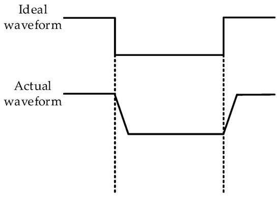
Figure 4.
Comparison diagram of ideal signal and actual signal.
Next, we will make a slight modification to Formula (3) to represent the actual situation where the signal edge is a steep slope shape:
The Fourier transform of Formula (5) now becomes the following:
When takes the value , equals . A 20 s BPC baseband signal frame can be regarded as a linear combination of 20 baseband signals with different a values and time-shifted by 0 to 20 s in the time domain. Therefore, the complete frame signal can be expressed as
After modulating a cosine carrier signal of 68.5 kHz into Equation (7), the frequency-domain representation is as follows:
MATLAB (version 23.2.0.2365128, R2023b) simulations of the BPC low-frequency time code generation process (based on Table 3) are shown in Figure 5 and Figure 6.
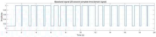
Figure 5.
Time-domain signal simulation schematic of BPC LF time code signal.
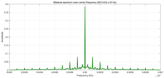
Figure 6.
BPC LF time code signal spectrum near carrier frequency (68.5 KHz).
It can be observed that the baseband signal spectrum is concentrated in the low-frequency range. The aperiodic pulse train results in a continuous (non-harmonic) spectral distribution. Furthermore, due to the combination of varying duty cycles in the time-domain signal, complex sideband structures are generated around the center frequency. From a phase perspective, continuous phase variation occurs near the carrier frequency, while phase jumps may appear at frequency points corresponding to pulse edges. Through the analysis and simulation of the BPC low-frequency time code generation process, we can understand its time-domain, frequency-domain, and phase characteristics. This facilitates the further optimization of the signal generator design and simplifies signal evaluation and monitoring.
To convert the BPC time code in the format of Equation (6) into the modulated signal of Equation (8), a signal generation module must be designed. This module performs frequency synthesis and high-precision timing functions, requiring communication with the time code generation module via RAM bus to receive BPCs while simultaneously acquiring external standard 10 MHz frequency and 1PPS signals through serial interfaces [16]. Considering that this design can be transformed into a BPC signal receiver and tested in modules without changing the hardware, the SoC chip is not considered for the design for the time being.
The module employs DDS (Direct Digital Synthesis) and PLL (Phase-Locked Loop) technologies to synthesize required frequencies such as 68.5 MHz and 68.5 kHz. Additionally, it synchronizes and calibrates local time based on the external 1PPS signal. These processes involve extensive digital computations, necessitating hardware implementation on an FPGA chip. The SPARTAN-6 XC6SLX9 chip from Xilinx, a cost-effective and low-power FPGA, features 102 user I/O pins and 576 Kb of RAM, making it fully capable of supporting the aforementioned computational tasks.
2.3. Design of Peripheral Analog Circuit Module
To power the system and enable signal D/A conversion, the peripheral analog circuit must meet the following power requirements for the core chips. Table 6 shows the power supply requirements of the chips.
Table 6.
Chip power supply requirements.
The system employs an external power supply of ±12 V and 5 V, along with voltage regulators LM317AEMP, AMS1117-3.3, and AMS1117-1.2. Two LM317AEMP regulators step down +12 V to +6 V and −12 V to −6 V, respectively. The AMS1117-3.3 and AMS1117-1.2 regulators convert 5 V to 3.3 V and 1.2 V, powering the ARM and FPGA chips while driving LED indicators.
The DAC module is responsible for converting the 12-bit digital BPC low-frequency time code signal into an analog output with adjustable amplitude. The AD5445 chip is a high-bandwidth and high-precision multiplicative digital-to-analog converter. It features 12-bit resolution, fully matching the requirements of BPC signal generation. Meanwhile, its high bandwidth and fast parallel interface meet the transmission needs of high-frequency waveform generation. In terms of cost, it is also relatively low compared to other chips. For this reason, the AD5445 chip is selected, working in conjunction with external operational amplifiers to achieve the D/A conversion function [17].
The overall system block diagram of the BPC low-frequency time code signal generator is shown in Figure 7, and the physical implementation of the module on the PCB is presented in Figure 8.
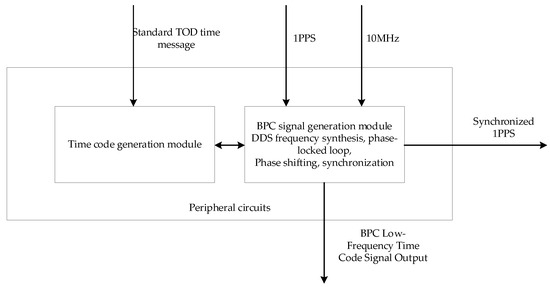
Figure 7.
BPC low-frequency time code signal generator system block diagram.
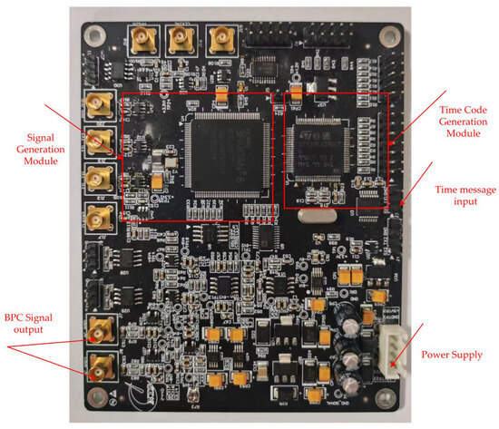
Figure 8.
PCB schematic diagram of BPC low-frequency time code signal generator.
3. Algorithm Design for BPC Low-Frequency Time Code Generator
3.1. BPC Signal Generation Algorithm Design
The signal generation algorithm is mainly divided into two parts: the ARM chip algorithm and the FPGA algorithm. The ARM chip is developed on the Keil μVision5 platform using C and C++ programming languages. The software flowchart is shown in Figure 9. The software part of the ARM chip is primarily divided into three threaded operations, ordered by priority from highest to lowest: the interruption triggered by TOD standard time data from USART1 serial port, the interruption triggered by the IRQ second signal, and the interruption triggered by the status IRQ second signal. After being powered on, the program automatically performs initialization. Once initialization is complete, the program enters the main loop and begins detecting the three interrupt signals.
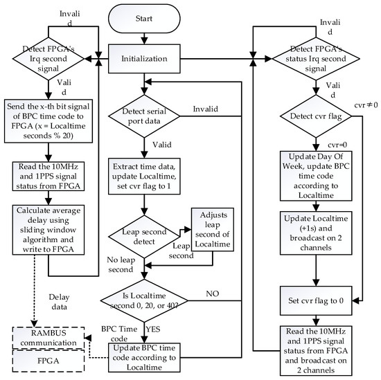
Figure 9.
Algorithm flowchart of time code generation module.
When valid USART1 serial data is detected, the program extracts the time information and updates all fields of the system’s local time, Localtime, except for the day of the week. It then sets the cvr flag to 1. The purpose of the cvr flag is to distinguish between internal and external time sources and prevent duplicate updates of Localtime. The program then checks for leap seconds and adjusts Localtime accordingly. Finally, the program updates the BPC time code array composed of 20 char-type variables based on Localtime. Note that the BPC time code is only updated when the Localtime second value is 0, 20, or 40, because the BPC low-frequency time code signal has a frame duration of 20 s and only starts at the 0th, 20th, or 40th second of each minute.
When the program detects the IRQ second signal, it initiates RAM bus communication with the FPGA via address mapping. First, it sends the x-th BPC time code, where x denotes the Localtime second value modulo 20. This ensures that when the BPC time code is continuously and cyclically transmitted, the normal timing of Localtime remains unaffected. The program then reads the delay measurement between the local and external 1PPS signals from the FPGA, calculates the average rate of change cntMean of adjacent measurements using a sliding window algorithm, and writes the compensated delay value to the FPGA. Additionally, this section includes a fault detection feature. By setting a watchdog counter for the communication interface, the program will issue a fault alarm signal if communication fails for a certain period [18,19,20].
When the program detects the status IRQ second signal, it checks the value of the cvr flag. If cvr = 0, it indicates that the external time has not yet updated Localtime, and the program will automatically update Localtime (typically by adding 1 s) before setting the cvr flag to 0. Furthermore, this section reads the difference between the 10 MHz clock and the 1PPS signal from the FPGA and broadcasts it externally (to the host computer or display) via a dual-channel interface [11].
The FPGA chip algorithm part is developed on the ISE14.7 platform using the Verilog language. The main modules are shown in Figure 10 and divided into four parts: 1PPS signal processing, clock signal processing, BPC signal generation, and the RAM bus communication module. The system uses an external standard 10 MHz clock as the main clock and an onboard 25 MHz crystal oscillator as the backup clock. The onboard 25 MHz crystal oscillator is synchronized and multiplied to generate a local 100 MHz clock source. This local clock source provides clock services for two Verilog modules: second signal synchronization monitoring and RAM bus communication. It also serves as a backup when the external 10 MHz signal fails, ensuring normal system operation. After the external 10 MHz differential clock signal is input, it is synthesized into a 68.5 MHz clock through DDS and then divided into different frequencies such as 100 MHz and 68.5 kHz through a PLL phase-locked loop, providing clock services for other Verilog modules [21].
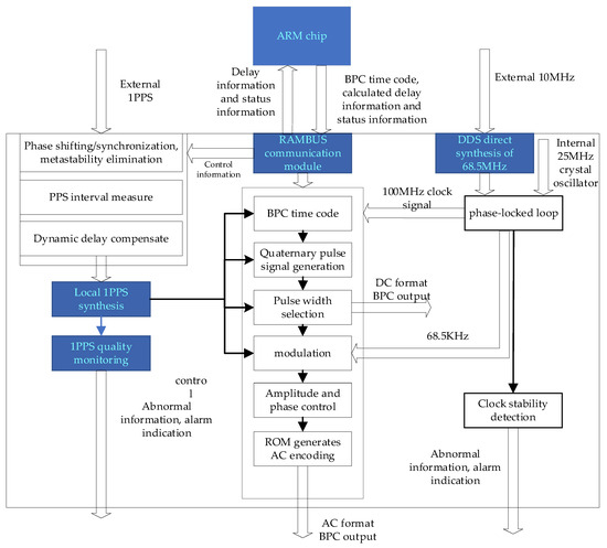
Figure 10.
Software architecture diagram of BPC signal generation module.
The 1PPS processing module receives the external standard 1PPS signal and also generates a local 1PPS signal based on the 100 MHz clock. After delay compensation with the external clock and metastability elimination, the local clock signal provides synchronous control signals for BPC signal generation and Localtime, ensuring the accuracy of local time and the synchronization of BPC signal generation [22,23].
The structure of the RAM bus communication module is illustrated in Figure 11. It adopts an address/data multiplexing mode to achieve bidirectional communication between the ARM and FPGA. The BPC time code generation module produces multiple negative pulse signals with varying pulse widths, selecting the corresponding output based on data received from the ARM. At this stage, the generated BPC signal is in DC format. By superimposing a 68.5 kHz carrier wave, the AC-format BPC signal is generated for output. During modulation, the ARM can send control signals to adjust the amplitude and phase of the BPC signal, with an amplitude resolution of 0.1 V and a phase resolution of 1 ns. Figure 11 shows the communication module structure of RAMBUS.
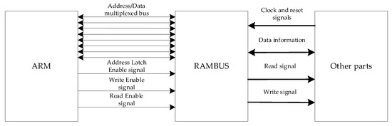
Figure 11.
RAMBUS communication module structure.
3.2. Other Algorithm Designs
3.2.1. Time Delay Calibration Algorithm Design
Since the internal 1PPS signal is generated using a counter, it exhibits significant errors without external calibration. Therefore, it is necessary to measure the time difference between the internal 1PPS and the external standard source and perform negative feedback adjustment compensation through calculation to ensure the accuracy of the internal 1PPS. This is shown in Figure 12.
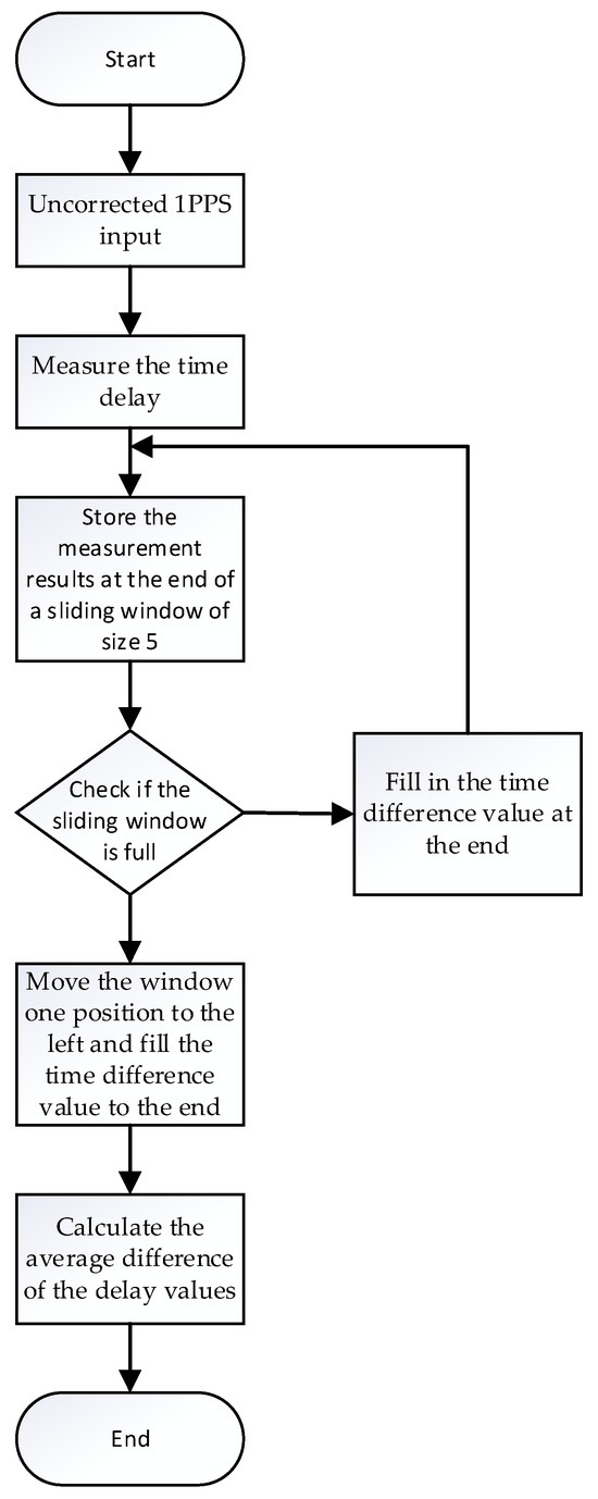
Figure 12.
Time delay calibration algorithm flowchart.
The time difference calculation employs a sliding window algorithm with a window size of 5. The window stores 1PPS time difference measurements read from the FPGA as x [0] to x [4]. By traversing adjacent time difference values within the window, the differential x [i + 1] – x [i] is computed and summed to obtain the total differential sum. Dividing this sum by the window length minus 1 yields the average time difference change rate, cntMean, which is used to predict the next time difference. Finally, the current measured value PpsDelayMeasure is added to the mean cntMean to derive the corrected time difference PpsDelayMeasureTmp, which is sent back to the FPGA.
This sliding window algorithm draws inspiration from the flow control mechanism of the TCP sliding window protocol [24]. By calculating the mean of multiple data points within the window, it smooths out instantaneous measurement errors, enhancing the stability of time difference measurements. It achieves high-precision time difference measurement and dynamic correction, making it suitable for hardware timing control systems with stringent real-time requirements. Figure 13 shows the effect of time delay calibration. Figure 14 shows the comparison of time delay variation before and after using sliding window algorithm.
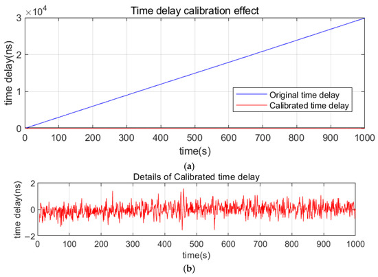
Figure 13.
(a) Time delay calibration effect using sliding window algorithm. (b) Details of calibrated time delay variation.
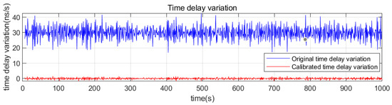
Figure 14.
Comparison of time delay variation before and after using sliding window algorithm.
3.2.2. DDS Algorithm Design
The design of the traditional BPC low-frequency time code signal generator is based on analog signals. In this paper, when synthesizing the 68.5 kHz signal, the method based on the on-board crystal oscillator was adopted. The 68.5 kHz frequency was synthesized through PLL, but the frequency switching speed was relatively slow and the frequency resolution was low. Therefore, this design adopts Direct Digital Synthesis (DDS) to generate a frequency of 68.5 MHz and then divides it to 68.5 kHz through PLL. The main process is as Figure 15.
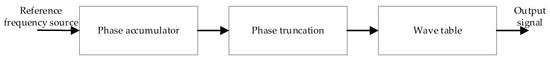
Figure 15.
DDS process flow diagram.
Compared with the traditional methods, its main advantages are shown in Table 7.
Table 7.
A comparison of the advantages of the two methods.
The function of the phase accumulator is to accumulate the frequency tuning word (FTW) under clock drive, where
where N denotes the bit width of the phase accumulator, typically set to 32 bits.
The truncated phase value (taking the first M bits) is input to the waveform lookup table (LUT), which retrieves and outputs the stored waveform samples (generally sinusoidal). The relationship between the DDS input clock frequency (f_clk) and output frequency (f_out) is given by the following:
The frequency resolution is as follows:
In FPGA, the DDS IP core can be invoked to flexibly generate high-precision frequency signals, offering advantages such as simplified design, high frequency resolution, and minimal frequency deviation compared to traditional architectures. For generating digital-format carrier signals, this design incorporates amplitude control parameters and a delay module [25,26]. The amplitude control parameters digitally regulate the 12-bit output signal, supplemented by an analog adjustment method using variable resistors in the D/A module to achieve precise signal amplitude control. The delay module receives phase modulation parameters from the ARM, enabling the accurate phase control of the output signal. Figure 16 shows BPC low-frequency time code signals with different amplitudes and modulation ratios synthesized using DDS.
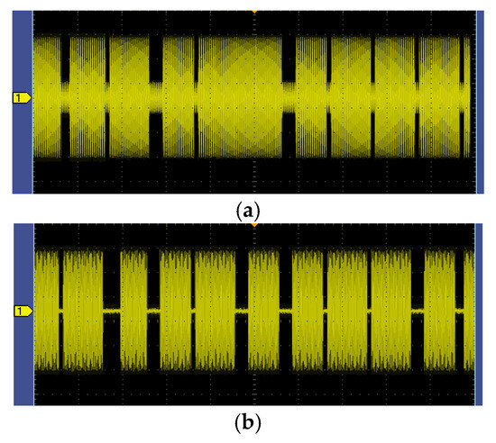
Figure 16.
DDS modulated waveform effect: (a) 10 V, 25% modulation depth; (b) 5 V, 10% modulation depth.
4. Testing BPC Low-Frequency Time Code Signal Generator
4.1. Test Methods and Test Indicators
Since the BPC low-frequency time code signal generator was designed with its potential use as a receiver in mind, its hardware design allows for bidirectional signal flow. Without modifying the hardware, the device can be converted into a BPC low-frequency time code signal receiver for signal transmission and reception testing by making software adjustments and integrating a demodulation module. Figure 17 shows a schematic diagram of the test system structure. The generator is externally connected to the standard time source, standard 1PPS signal, and standard 10 MHz clock signal source from the National Time Service Center of the Chinese Academy of Sciences. The transmitting and receiving antennas are placed approximately 3 m apart. The AC-to-DC module performs envelope detection on the received AC-format BPC signal, converting it into a DC-format BPC signal. The DC signal processing module then carries out time synchronization and signal decoding, using the received 1PPS signal as a reference to calibrate the local 1PPS signal. A counter converts the DC-format BPC signal into the corresponding BPC time code. This part of the design is based on the generator’s FPGA module and transmits the data to the ARM chip via the RAM bus. The ARM chip translates the quaternary BPC time code into time information and outputs it to the PC host software (SSCOM, v5.13.1). Given the importance of BPC signals in the field of radio-controlled clocks, the generator’s signal can be directly transmitted to commercial radio-controlled clocks to verify its actual timekeeping performance [27,28].
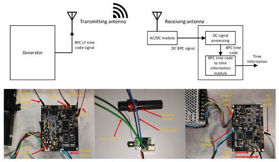
Figure 17.
Test system structure diagram.
The signal quality evaluation of low-frequency time code timing signals primarily consists of four levels of indicators, ranked by priority as follows: carrier frequency, negative pulse duration validity, signal field strength, and modulation depth. These four evaluation metrics reflect both the correctness and acceptability of the transmitted low-frequency time code timing signal. Since this study focuses only on the laboratory testing of the generator, the field strength indicator is not considered for now. Table 8 shows the variation ranges and evaluation criteria for each parameter. Here, σ represents the standard deviation of n data points within the sampling period, where , and k denotes a control parameter set to 3. Negative pulse duration validity refers to the duration of the demodulated low-level signal, which must be one of the following values: 0.1 s, 0.2 s, 0.3 s, or 0.4 s.
Table 8.
Signal quality evaluation parameter table [27,29].
4.2. Test Results and Analysis
The Shangqiu BPC low-frequency time code transmission station operates from 9:00 to 17:00 and 21:00 to 5:00. To avoid interference from Shangqiu’s signals and other electromagnetic disturbances affecting this experiment, the tests were conducted from 5:30 to 8:30 on the early morning of 3 May 2025 Beijing time, evaluating the signal integrity, carrier frequency, phase, and modulation depth of the generated signals.
The BPC low-frequency time code signal generator produced both AC and DC format BPC signals. Oscilloscope measurements of a complete frame of the BPC signal are shown in Figure 18a,b. As mentioned in Section 2.2, since real-world signal generation cannot achieve perfect rising/falling edges, the negative pulse edges inevitably exhibit a steep slope-like structure. Figure 18c illustrates this slope characteristic.
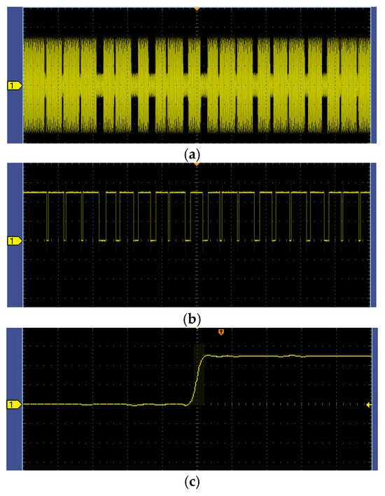
Figure 18.
One frame of BPC low-frequency time code signal: (a) AC-format BPC signal measured diagram, (b) DC-format BPC signal measured diagram, (c) steep edge structure of negative pulse.
A spectrum analysis of the BPC signal was performed using the oscilloscope’s FFT function, with results consistent with Equations (6) and (9), and the simulation outcomes, as shown in Figure 19.
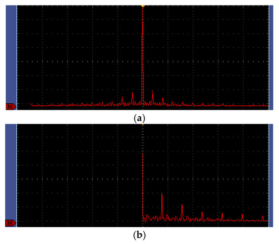
Figure 19.
BPC signal spectrum analysis diagram: (a) AC-format BPC signal measured spectrum diagram near 68.5 KHz; (b) DC-format BPC signal measured spectrum diagram near 0 Hz.
This study analyzed the selected 3 h low-frequency time code signal by grouping it into 5 min intervals, calculating the average values of carrier frequency and modulation depth across 61 groups, and recording phase variations. The results are shown in Figure 20. We simultaneously monitor the number of received time messages to verify the integrity of the time code and the effectiveness of the negative pulse duration validity. The results are shown in Table 9 and Table 10.
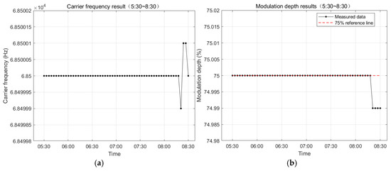
Figure 20.
Signal quality evaluation results: (a) carrier frequency result; (b) modulation depth result.
Table 9.
Time message monitoring results.
Table 10.
Signal quality evaluation result.
Regarding the abnormal fluctuations in carrier frequency and modulation depth observed around 8:15–8:30, several hypotheses are proposed: 1. temperature rise due to continuous system operation; 2. potential adjacent noise from laboratory LED drivers (switching frequency: 50 kHz–1 MHz); and 3. noise induced by power line communication (50 kHz–150 kHz). Overall, the generated signals demonstrate integrity, with carrier frequency, phase, and modulation depth all falling within valid ranges, indicating satisfactory performance [12].
Figure 21 shows the results of adjusting a radio-controlled clock to a specific time using time-source information sent from the host computer. The radio-controlled clock was developed by the National Time Service Center of the Chinese Academy of Sciences. The radio-controlled clock successfully received the BPC low-frequency time code timing signal generated by the transmitter and was successfully calibrated. This confirms the practical applicability of the BPC low-frequency time code signal generator in laboratory environments.
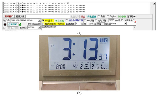
Figure 21.
Test results of BPC LF time code signal reception by radio-controlled clock in laboratory environment. (a) Time information sent by host computer. (b) Radio-controlled clock receiving BPC LF time code signal and calibration results (“下午”: afternoon; “上午”: morning; “月”: month; “日”: day; “温度”: temperature).
5. Conclusions
This study analyzed the generation process of BPC low-frequency time code timing signals and implemented a BPC low-frequency time code timing signal generation system based on the ARM-FPGA architecture from both hardware and software aspects. Compared with the traditional BPC low-frequency time code timing system based on analog circuits, this system is implemented in a digital way. It has independent modules, convenient maintenance and testing, adjustable indicators such as leap second, output signal amplitude, output signal modulation depth, etc. Meanwhile, the sliding window delay calibration method is used to increase the second signal delay to about 1 ns. The DDS technology was adopted in frequency generation, resulting in a more stable and accurate 68.5 kHz signal.
The test results show that the system has good stability in terms of carrier frequency, phase, modulation depth and other indicators and can successfully synchronize the radio control clock, which proves the practical value of the system and lays a foundation for subsequent field tests.
This research not only implemented the BPC low-frequency time code timing generator in hardware, providing a platform for subsequent signal system research, but also reduced the delay at the transmitting end and optimized the overall effect of the low-frequency time code signal timing system.
The experimental results reveal some problems existing in the system, such as being vulnerable to electromagnetic interference from various environmental sources when the transmission power is weak.
In addition, since the only LF BPC time code timing station in China is currently in normal operation, using it for testing will have a significant impact on the timing effect. Therefore, we are temporarily unable to conduct large-scale tests on the generator. However, in the future, we will improve the experimental methods and strive to conduct experiments with higher transmission power under conditions that cause more severe electromagnetic interference to the generator.
Author Contributions
Conceptualization, H.C.; Methodology, H.C. and K.Y.; Software, H.C., X.G., Z.Z. and Y.L.; Validation, Z.Z.; Formal analysis, H.C. and Z.Z.; Investigation, Y.X. and K.Y.; Resources, X.G.; Data curation, X.G.; Writing—original draft, H.C.; Writing—review & editing, J.W., X.G., D.Z. and Y.X.; Visualization, H.C. and Y.L.; Supervision, J.W. and D.Z.; Project administration, J.W. and D.Z.; Funding acquisition, J.W. All authors have read and agreed to the published version of the manuscript.
Funding
This research received no external funding.
Data Availability Statement
All the necessary data are included in the article.
Conflicts of Interest
The authors declare no conflicts of interest.
References
- Wang, X.; Li, B.; Zhao, F.; Luo, X.; Huang, L.; Feng, P.; Li, X. Variation of Low-Frequency Time-Code Signal Field Strength during the Annular Solar Eclipse on 21 June 2020: Observation and Analysis. Sensors 2021, 21, 1216. [Google Scholar] [CrossRef]
- Zhao, F.; Feng, P.; Qi, Z.; Cheng, L.; Wang, X.; Huang, L.; Liu, Q.; Chen, Y.; Ren, X.; Hua, Y. Investigation on the Impact of the 2022 Luding M6.8 Earthquake on Regional Low-Frequency Time Code Signals in Northern China. Atmosphere 2024, 15, 1419. [Google Scholar] [CrossRef]
- Cheng, W.; Xu, W.; Gu, X.; Wang, S.; Wang, Q.; Ni, B.; Lu, Z.; Xiao, B.; Meng, X. A Comparative Study of VLF Transmitter Signal Measurements and Simulations during Two Solar Eclipse Events. Remote Sens. 2023, 15, 3025. [Google Scholar] [CrossRef]
- Yin, K.; Wu, J.; Ning, R.; Chen, Y.; Liu, Q.; Wang, K. Preliminary Evaluation and Analysis of Differential Technology Performance of eLoran Timing System. Electronics 2025, 14, 789. [Google Scholar] [CrossRef]
- Xu, W.; Zhang, P.; Wang, L.; Yan, C.; Chen, J. Performance Assessment of Undifferenced GPS/Galileo Precise Time Transfer with a Refined Clock Model. Remote Sens. 2025, 17, 1910. [Google Scholar] [CrossRef]
- Lee, D.; Hwang, S.S. Enhanced Real-Time Onboard Orbit Determination of LEO Satellites Using GPS Navigation Solutions with Signal Transit Time Correction. Aerospace 2025, 12, 508. [Google Scholar] [CrossRef]
- Jin, X.; Hua, Y. Application of PN Code in Time Delay Measurement of Telephone Network. Sensors 2025, 25, 241. [Google Scholar] [CrossRef] [PubMed]
- Guo, Y.; Gao, S.; Pan, Z.; Wang, P.; Gong, X.; Chen, J.; Song, K.; Zhong, Z.; Yue, Y.; Guo, L.; et al. Advancing Ultra-High Precision in Satellite–Ground Time–Frequency Comparison: Ground-Based Experiment and Simulation Verification for the China Space Station. Remote Sens. 2023, 15, 5393. [Google Scholar] [CrossRef]
- Tu, R.; Zhang, P.; Zhang, R.; Liu, J.; Lu, X. Modeling and Assessment of Precise Time Transfer by Using BeiDou Navigation Satellite System Triple-Frequency Signals. Sensors 2018, 18, 1017. [Google Scholar] [CrossRef]
- Huang, L.; Qi, Z.; Shi, S.; Chen, Y.; Zhao, F.; Wang, X.; Zhu, F.; Li, X.; Feng, P. Study on the Impact of C-Class Solar Flares on Low-Frequency Signal Propagation and Ionospheric Disturbances. Atmosphere 2025, 16, 154. [Google Scholar] [CrossRef]
- Bai, Y.; Wu, G.; Xu, L. A Study of Low Frequency Time-code Receiver High Precision Timing. J. Electron. Meas. Instrum. 2006, 20, 102–105. [Google Scholar] [CrossRef]
- Luo, X.; Feng, P. Research on Low Frequency Time Code Interference Detection Based on Weighted Detection. J. Time Freq. 2023, 46, 298–307. [Google Scholar] [CrossRef]
- Feng, P. Study on the Additional Spread Spectrum Modulation Technique in Low-Frequency Time-Code Timing Service System; University of Chinese Academy of Sciences: Beijing, China, 2008. [Google Scholar]
- Susa, H.; Mori, K.; Sugawara, M.; Matsuzawa, A. SWA: SoftWare for Analog Design Automation. Chips 2024, 3, 379–394. [Google Scholar] [CrossRef]
- Zagan, I.; Găitan, V.G. BIoT Smart Switch-Embedded System Based on STM32 and Modbus RTU—Concept, Theory of Operation and Implementation. Buildings 2024, 14, 3076. [Google Scholar] [CrossRef]
- Huang, L. Research on Key Technology for the Design of Low-Frequency Time-Code Time Signal Structure; University of Chinese Academy of Sciences: Beijing, China, 2023. [Google Scholar]
- Lim, X.Y.; Teo, B.C.T.; Navaneethan, V.; Lim, W.C.; Siek, L. Design and Analysis of a Novel 12-Bit Current-Steering–Capacitive Digital-to-Analog Converter. J. Low Power Electron. Appl. 2025, 15, 9. [Google Scholar] [CrossRef]
- Lai, W.; Li, S. Design of BPM HF signal based on DDS. GNSS World China 2021, 46, 16–21. [Google Scholar] [CrossRef]
- Cui, H.; Wang, K.; Wu, J. Design and implementation of second pulse phase shifter based on DP83640. Navig. Position. Timing 2024, 11, 133–142. [Google Scholar] [CrossRef]
- Liu, Z. The Research on Applying Virtual Instrument Technology to Measure and Monitor Low-Frequency Time-Codes Time Service Signal; University of Chinese Academy of Sciences: Beijing, China, 2007. [Google Scholar]
- Tang, S.; Ke, J.; Wang, T.; Deng, Z. Development of a Miniaturized Frequency Standard Comparator Based on FPGA. Electronics 2019, 8, 123. [Google Scholar] [CrossRef]
- Yan, F. Design and Realization of Precise Time Interval Counter Based on FPGA and TDC-GPX2; University of Chinese Academy of Sciences: Beijing, China, 2018. [Google Scholar]
- Shen, C.-H.; Wu, Y.-H.; Chen, S.-J.; Yu, C.-Y. High-Speed-Recognition Artificial Intelligence Chip Based on ARM+FPGA Platform. In Proceedings of the 2024 IEEE 6th Eurasia Conference on IoT, Communication and Engineering, Yunlin, Taiwan, China, 15–17 November 2024; p. 33. [Google Scholar]
- Prajapati, J.I.; Das, R. Sliding Window-Based Randomized K-Fold Dynamic ANN for Next-Day Stock Trend Forecasting. Computation 2025, 13, 141. [Google Scholar] [CrossRef]
- Zhou, K.; Xu, Q.; Zhang, T. Optimized Design of Direct Digital Frequency Synthesizer Based on Hermite Interpolation. Sensors 2024, 24, 6285. [Google Scholar] [CrossRef] [PubMed]
- Xing, X.; Melek, W.; Wang, W. A Recursive Trigonometric Technique for Direct Digital Frequency Synthesizer Implementation. Electronics 2024, 13, 4762. [Google Scholar] [CrossRef]
- Wang, X. Research on Monitoring and Assessment Method of Low-Frequency Time-Code Signal Quality and Timing Performance; University of Chinese Academy of Sciences: Beijing, China, 2023. [Google Scholar]
- Guo, Y.; Rao, Y.; Wang, X.; Zou, D.; Shi, H.; Ji, N. Carrier Characteristic Bias Estimation between GNSS Signals and Its Calibration in High-Precision Joint Positioning. Remote Sens. 2023, 15, 1051. [Google Scholar] [CrossRef]
- Lin, D.; Yang, C.; Li, S. Analysis of the influence of modulation ratio on the transmission performance of low-frequency time code signals. Electron. Des. Eng. 2023, 31, 26–29. [Google Scholar] [CrossRef]
Disclaimer/Publisher’s Note: The statements, opinions and data contained in all publications are solely those of the individual author(s) and contributor(s) and not of MDPI and/or the editor(s). MDPI and/or the editor(s) disclaim responsibility for any injury to people or property resulting from any ideas, methods, instructions or products referred to in the content. |
© 2025 by the authors. Licensee MDPI, Basel, Switzerland. This article is an open access article distributed under the terms and conditions of the Creative Commons Attribution (CC BY) license (https://creativecommons.org/licenses/by/4.0/).