
High-Performance All-Optical Logic Gates Based on Silicon Racetrack and Microring Resonators


Abstract
1. Introduction
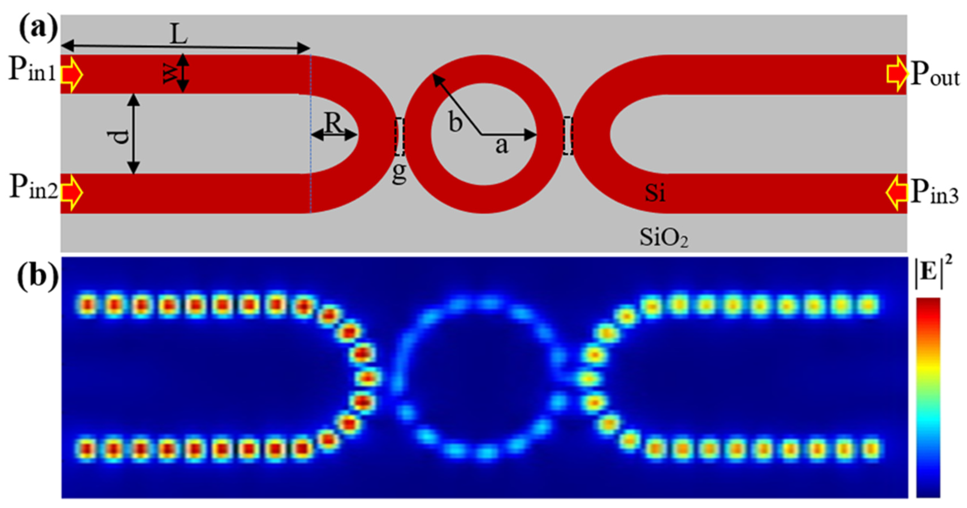
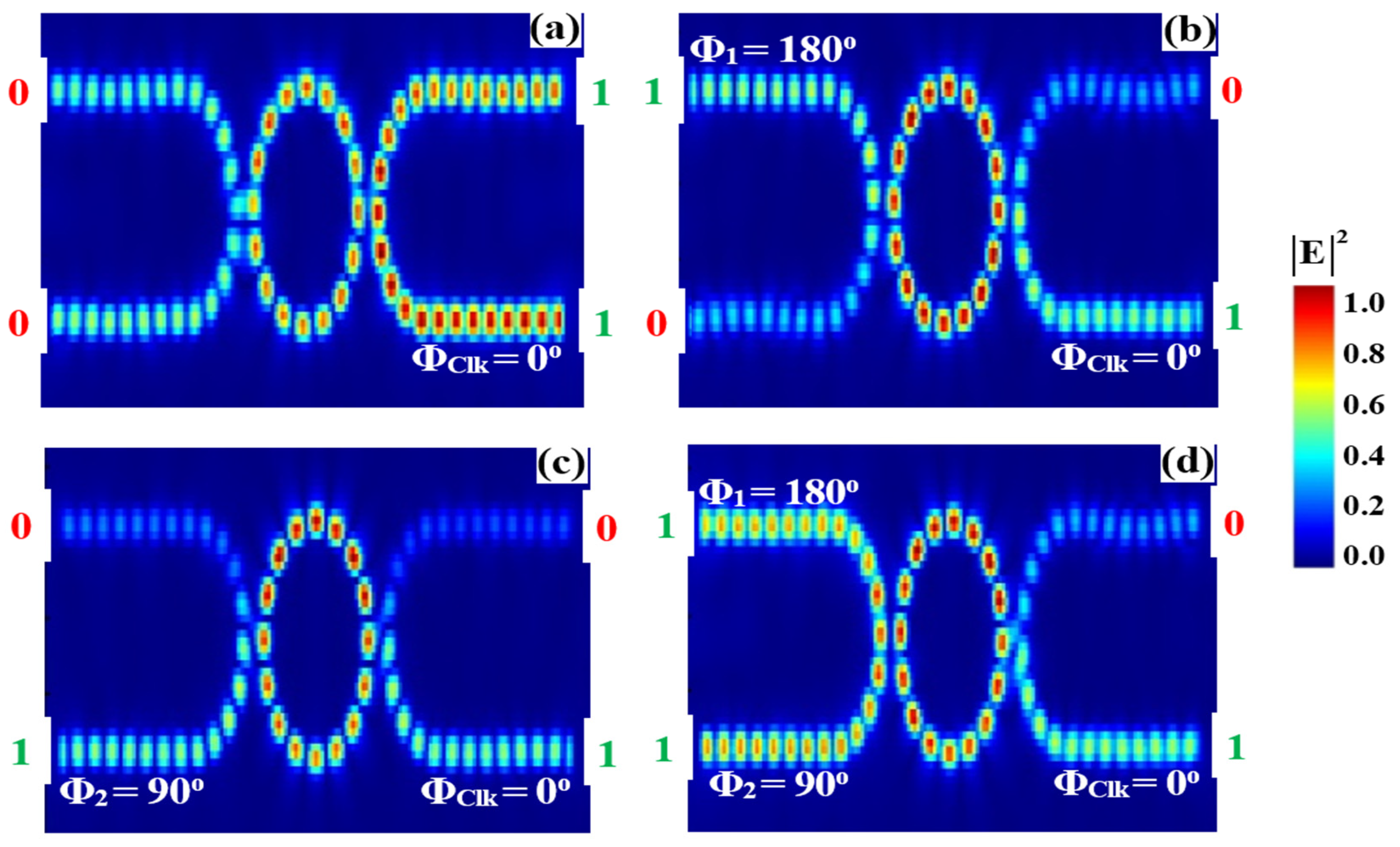
2. Racetrack–Ring Resonator Configuration
3. Implementation of Logic Gates
3.1. XOR
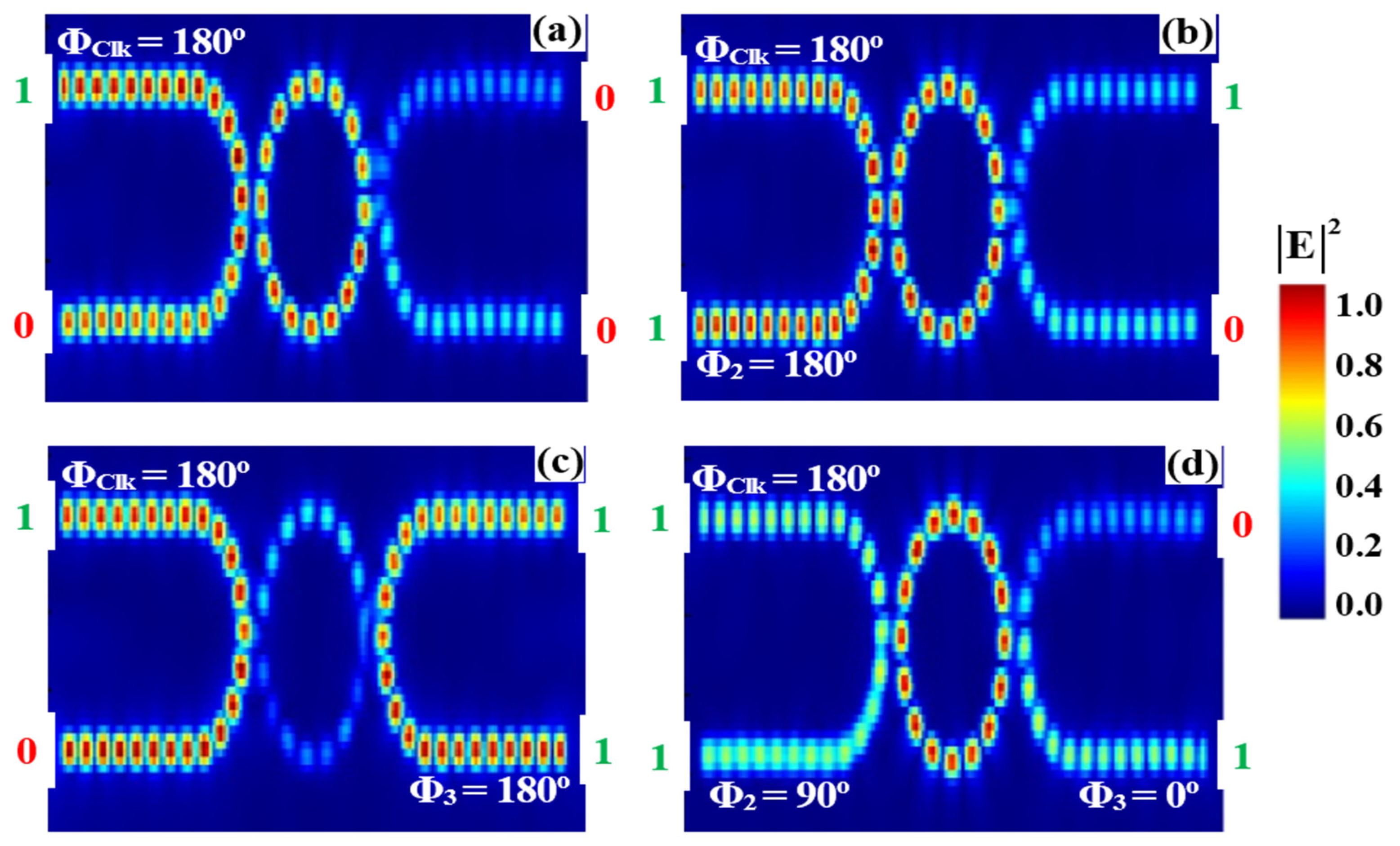
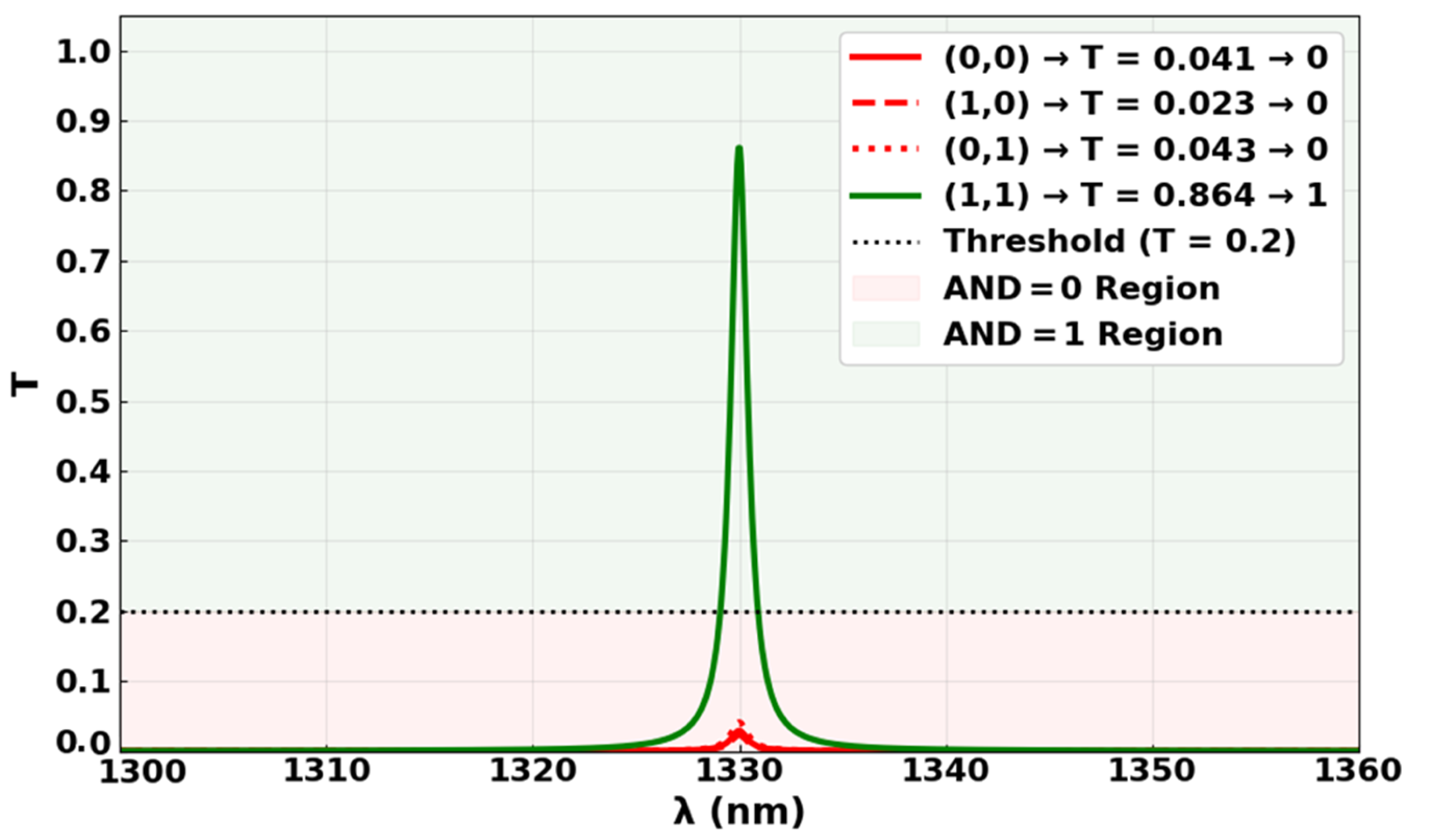
3.2. AND
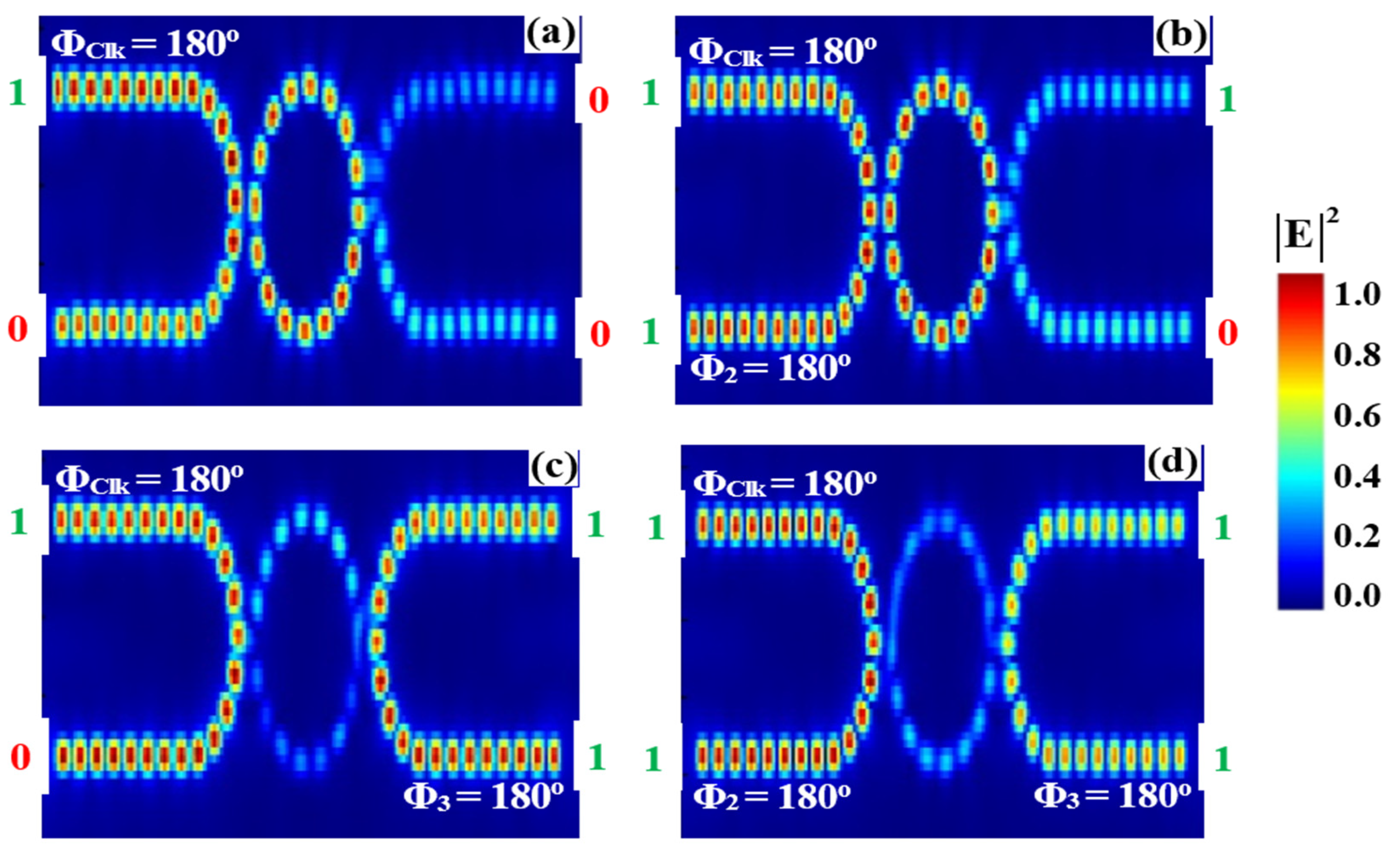
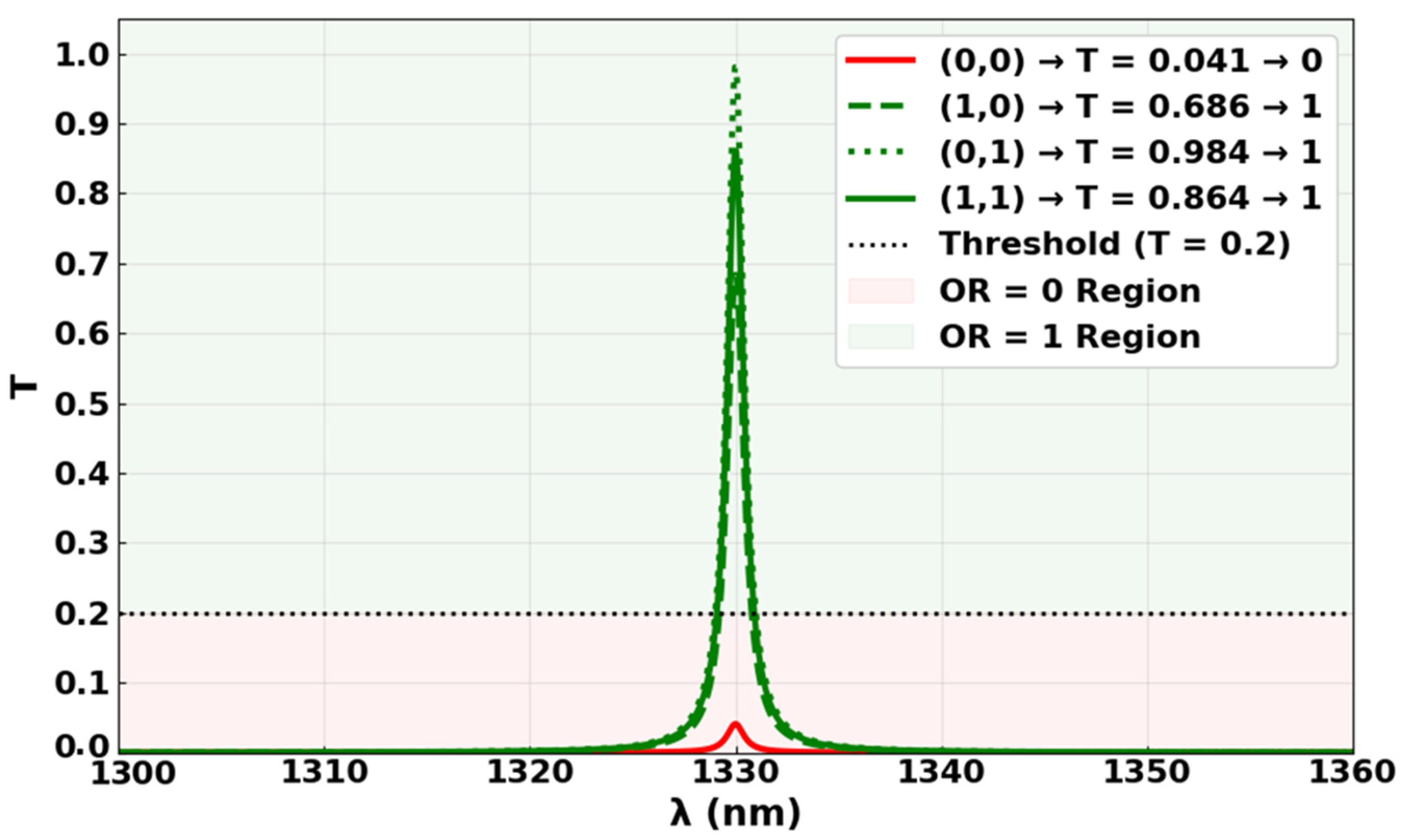
3.3. OR
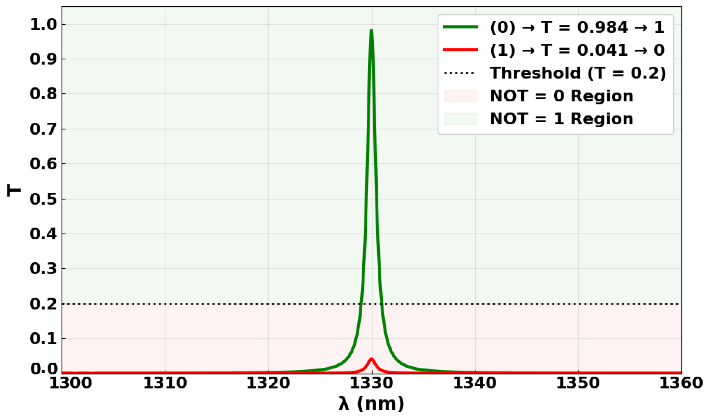
3.4. NOT
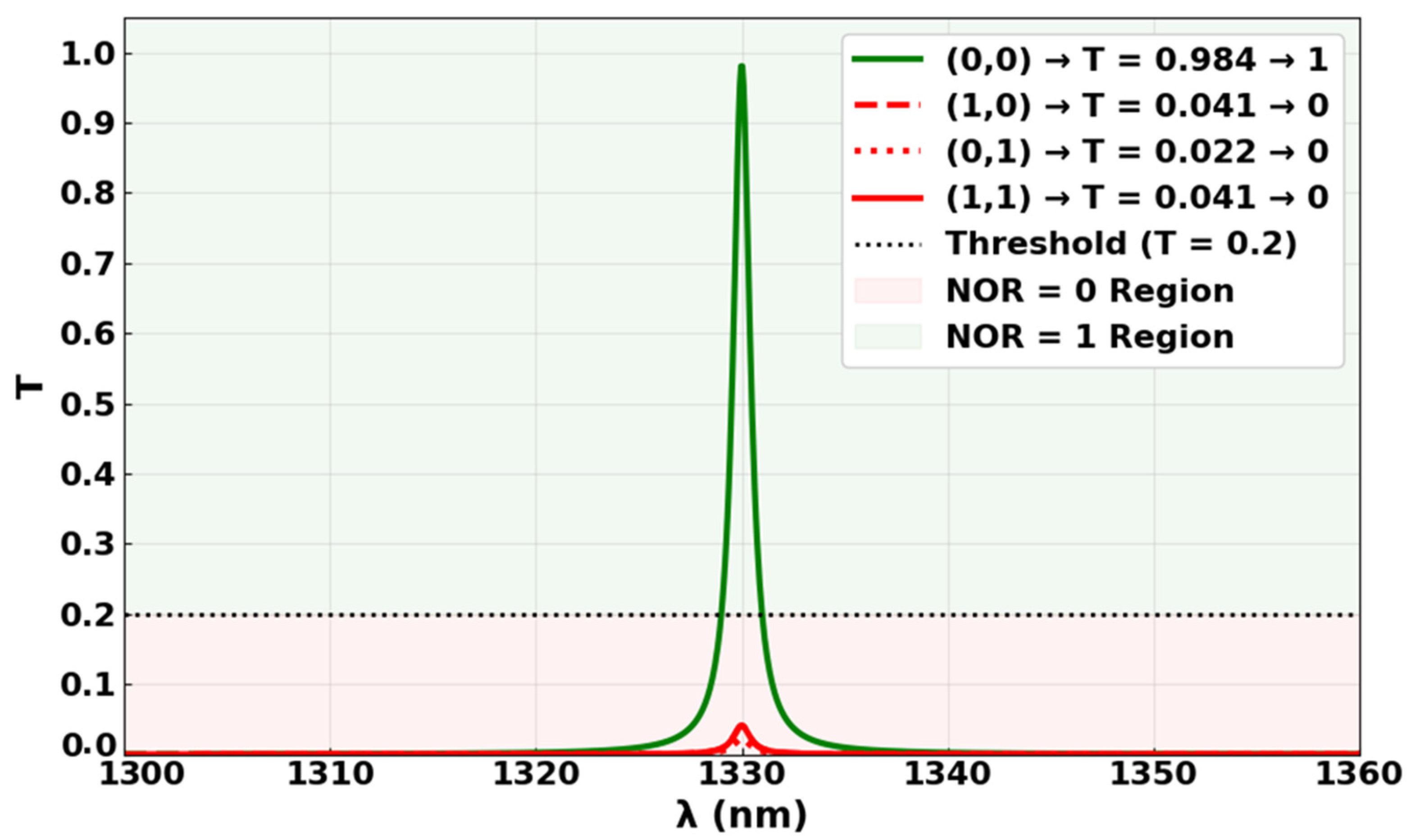
3.5. NOR
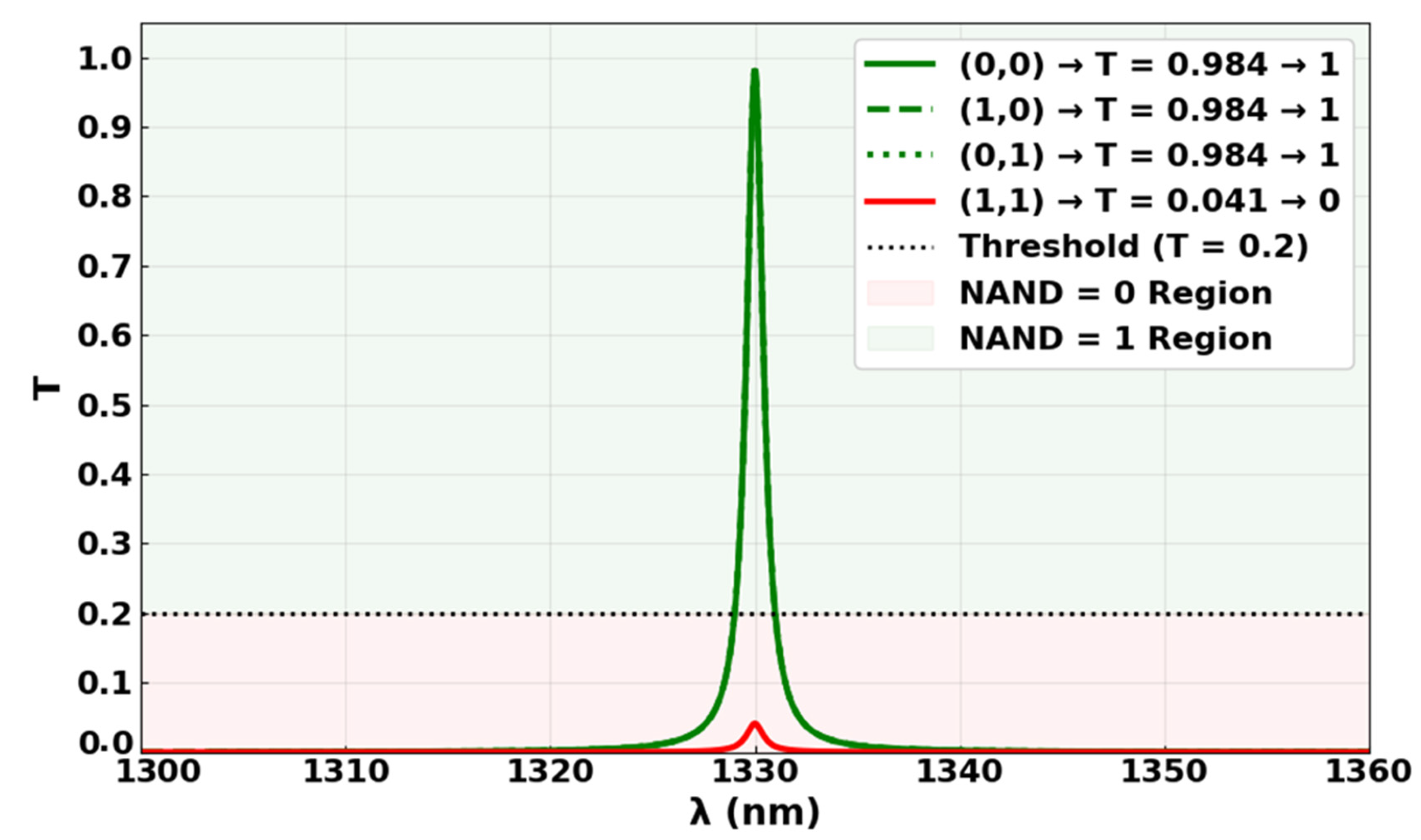
3.6. NAND
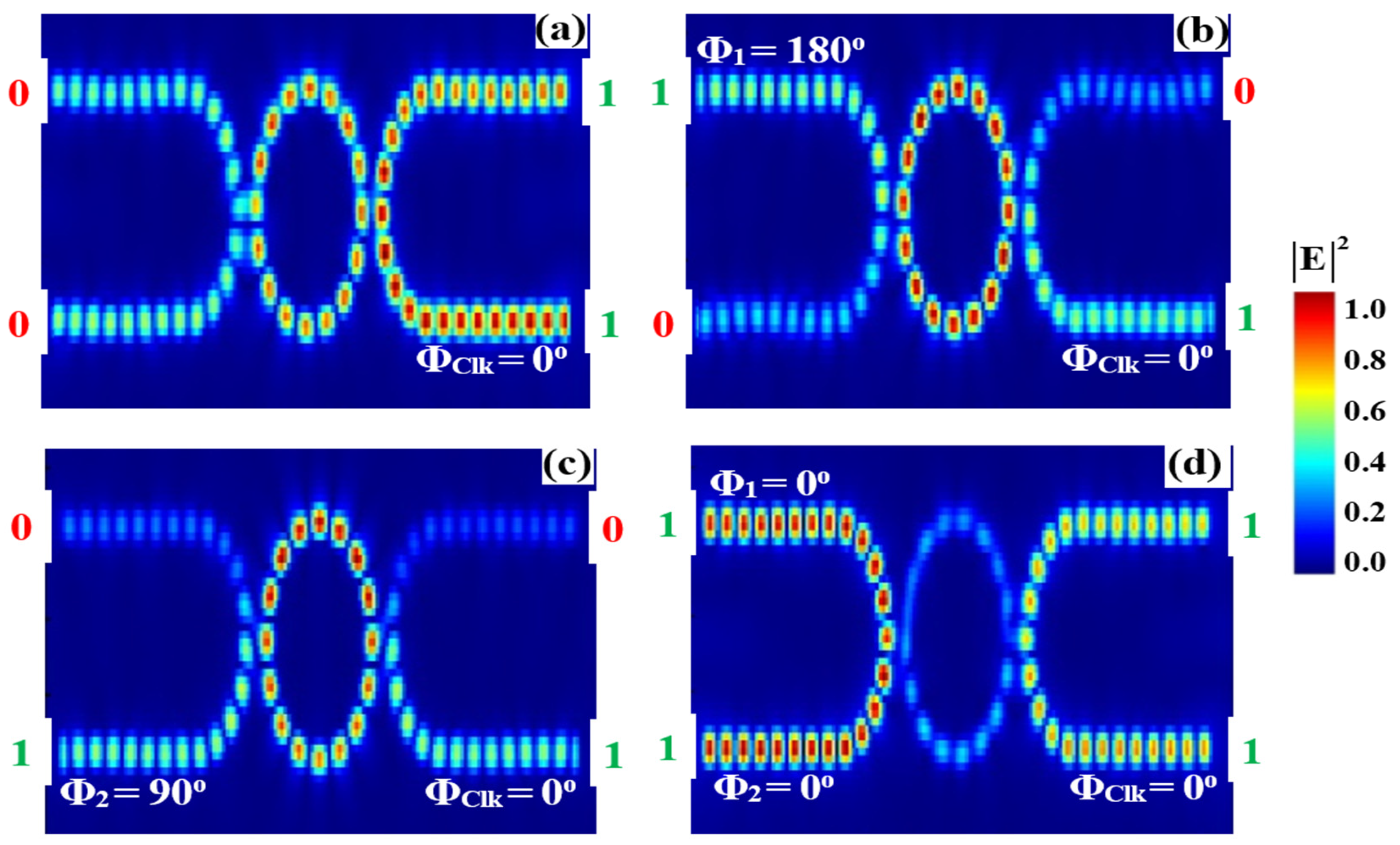
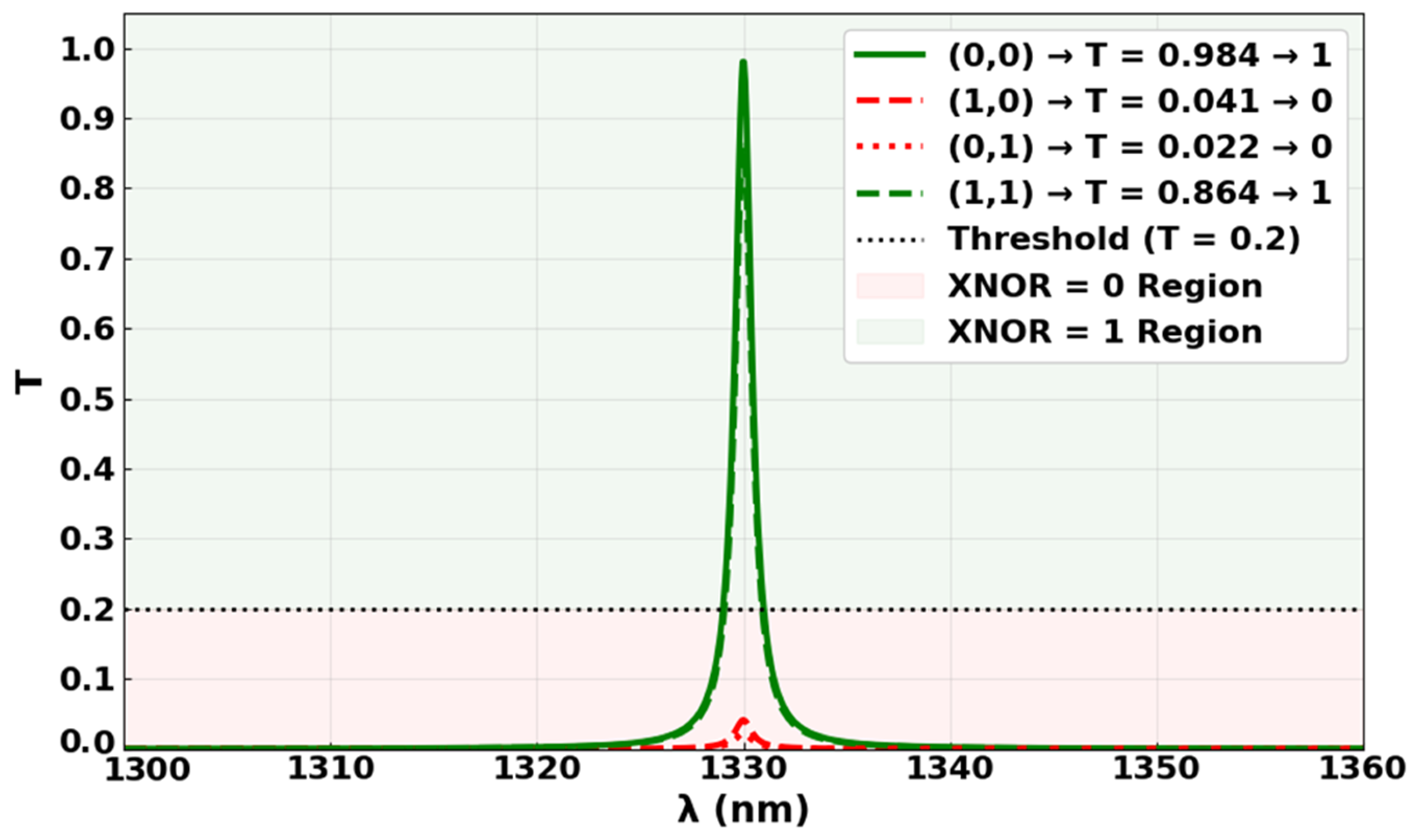
3.7. XNOR
4. Performance Comparison
- It achieves higher speed than most experimentally validated photonic gates, without compromising on CR.
- It avoids the metal losses and fabrication complexities associated with plasmonic platforms.
- It is fabrication-friendly, leveraging standard silicon photonic processes (e.g., SOI platforms), unlike inverse-designed or PhC-based devices requiring more exotic patterning.
- The racetrack-coupled microring structure provides enhanced resonant control and mode confinement, ensuring reliable, repeatable logic behavior with minimal design complexity.
5. CMOS-Compatible Fabrication and Logic Gate Performance
6. Conclusions
Author Contributions
Funding
Data Availability Statement
Conflicts of Interest
Abbreviations
| FDTD | finite-difference time domain |
| AOLGs | all-optical logic gates |
| CR | contrast ratio |
| Si | silicon |
| SiO2 | silicon dioxide |
| CMOS | complementary metal–oxide–semiconductor |
| T | normalized transmission |
| Q | quality factor |
| TE | transverse electric mode |
| b | ring outer radius |
| a | ring inner radius |
| w | ring width |
| R | bend radius |
| g | coupling gap |
| Clk | clock signal |
| CI | constructive interference |
| DI | destructive interference |
| τp | photon lifetime |
| λ | operating wavelength |
| FWHM | full width at half maximum |
| DUV | deep ultraviolet |
| ICP-RIE | inductively coupled plasma–reactive ion etching |
| PECVD | plasma-enhanced chemical vapor deposition |
References
- Zhang, F.; He, L.; Zhang, H.; Kong, L.-J.; Xu, X.; Zhang, X. Experimental realization of topologically-protected all-optical logic gates based on silicon photonic crystal slabs. Adv. Photonics Res. 2023, 17, 2200329. [Google Scholar] [CrossRef]
- He, L.; Zhang, F.; Zhang, H.; Kong, L.-J.; Zhang, W.; Xu, X.; Zhang, X. Topology-optimized ultracompact all-optical logic devices on silicon photonic platforms. ACS Photonics 2022, 9, 597–604. [Google Scholar] [CrossRef]
- Ono, M.; Hata, M.; Tsunekawa, M.; Nozaki, K.; Sumikura, H.; Chiba, H.; Notomi, M. Ultrafast and energy-efficient all-optical switching with graphene-loaded deep-subwavelength plasmonic waveguides. Nat. Photonics 2020, 14, 37–43. [Google Scholar] [CrossRef]
- Lipson, M. The revolution of silicon photonics. Nat. Mater. 2022, 21, 974–975. [Google Scholar] [CrossRef] [PubMed]
- Dai, D.; Liang, D.; Cheben, P. Next-generation silicon photonics: Introduction. Photon. Res. 2022, 10, NGSP1–NGSP3. [Google Scholar] [CrossRef]
- Baets, R.; Van Thourhout, D.; Bienstman, P.; Roelkens, G.; Dumon, P.; Bogaerts, W. Silicon photonics: Opportunities and challenges. In Asia Optical Fiber Communication and Optoelectronic Exposition and Conference; OSA Technical Digest (CD); Optica Publishing Group: Washington, DC, USA, 2008; p. SaH1. [Google Scholar]
- Jalali, B.; Fathpour, S. Silicon photonics. J. Light. Technol. 2006, 24, 4600–4615. [Google Scholar] [CrossRef]
- Li, F.; Chen, F.; Zhou, S.; Liu, J.; Yu, X.; Xia, Y.; Chen, Q.; Sui, X. Bit-scalable optical logic gates based on directed logic and micro-ring resonators. Opt. Commun. 2025, 587, 131901. [Google Scholar] [CrossRef]
- Kotb, A.; Wang, Z.; Chen, W. High-contrast and high-speed optical logic operations using silicon microring resonators. Nanomaterials 2025, 15, 707. [Google Scholar] [CrossRef] [PubMed]
- Kotb, A.; Zoiros, K.E.; Guo, C. High-performance all-optical logic operations using Ψ-shaped silicon waveguides at 1.55 μm. Micromachines 2023, 14, 1793. [Google Scholar] [CrossRef] [PubMed]
- Ji, X.; Roberts, S.; Corato-Zanarella, M.; Lipson, M. Methods to achieve ultra-high quality factor silicon nitride resonators. APL Photonics 2021, 6, 071101. [Google Scholar] [CrossRef]
- Xu, Q.; Lipson, M. All-optical logic based on silicon micro-ring resonators. Opt. Express 2007, 15, 924–929. [Google Scholar] [CrossRef] [PubMed]
- Kita, S.; Nozaki, K.; Takata, K.; Shinya, A.; Notomi, M. Ultrashort low-loss Ψ gates for linear optical logic on Si photonics platform. Commun. Phys. 2020, 3, 33. [Google Scholar] [CrossRef]
- Butt, M.A. Racetrack ring resonator-based on hybrid plasmonic waveguide for refractive index sensing. Micromachines 2024, 15, 610. [Google Scholar] [CrossRef] [PubMed]
- Al-Musawi, H.K.; Al-Janabi, A.K.; Al-abassi, S.A.W.; Abusiba, N.A.H.A.; Al-Fatlawi, N.A.H.Q. Plasmonic logic gates based on dielectric-metal-dielectric design with two optical communication bands. Optik 2020, 223, 165416. [Google Scholar] [CrossRef]
- Taengnoi, N.; Bottrill, K.R.H.; Thipparapu, N.K.; Umnikov, A.A.; Sahu, J.K.; Petropoulos, P. WDM transmission with in-line amplification at 1.3 μm using a Bi-doped fiber amplifier. J. Light. Technol. 2019, 37, 1826–1830. [Google Scholar] [CrossRef]
- Hazari, A.; Hsiao, F.C.; Yan, L.; Heo, J.; Millunchick, J.M.; Dallesasse, J.M. 1.3 μm optical interconnect on silicon: A monolithic III-nitride nanowire photonic integrated circuit. IEEE J. Quantum Electron. 2017, 53, 6300109. [Google Scholar] [CrossRef]
- Riechert, H.; Ramakrishnan, A.; Steinle, G. Development of InGaAsN-based 1.3 μm VCSELs. Semicond. Sci. Technol. 2002, 17, 892. [Google Scholar] [CrossRef]
- Wang, L.V.; Hu, S. Photoacoustic tomography: In vivo imaging from organelles to organs. Science 2012, 335, 1458–1462. [Google Scholar] [CrossRef] [PubMed]
- Smith, A.M.; Mancini, M.C.; Nie, S. Second window for in vivo imaging. Nat. Nanotechnol. 2009, 4, 710–711. [Google Scholar] [CrossRef] [PubMed]
- Agrawal, G.P. Fiber-Optic Communication Systems, 4th ed.; Wiley-Interscience: Hoboken, NJ, USA, 2010. [Google Scholar]
- Rani, P.; Kalra, Y.; Sinha, R.K. Design of all-optical logic gates in photonic crystal waveguides. Optik 2015, 126, 950–955. [Google Scholar] [CrossRef]
- Rachana, M.; Swarnakar, S.; Krishna, S.V.; Kumar, S. Design and analysis of an optical three-input AND gate using a photonic crystal fiber. Appl. Opt. 2022, 61, 77–83. [Google Scholar] [CrossRef] [PubMed]
- Priya, N.H.; Swarnakar, S.; Krishna, S.V.; Kumar, S. Design and analysis of a photonic crystal-based all-optical 3-input OR gate for high-speed optical processing. Opt. Quantum Electron. 2021, 53, 720. [Google Scholar] [CrossRef]
- Rao, D.G.S.; Swarnakar, S.; Palacharla, V.; Raju, K.S.R.; Kumar, S. Design of all-optical AND, OR, and XOR logic gates using photonic crystals for switching applications. Photonic. Netw. Commun. 2021, 41, 109–118. [Google Scholar] [CrossRef]
- Mostafa, T.S.; Mohammed, N.A.; El-Rabaie, E.M. Ultra-high bit rate all-optical AND/OR logic gates based on photonic crystal with multi-wavelength simultaneous operation. J. Mod. Opt. 2019, 66, 1005–1016. [Google Scholar] [CrossRef]
- Pan, D.; Wei, H.; Xu, H. Optical interferometric logic gates based on metal slot waveguide network realizing whole fundamental logic operations. Opt. Express 2013, 21, 9556. [Google Scholar] [CrossRef] [PubMed]
- Bian, Y.; Gong, Q. Compact all-optical interferometric logic gates based on one-dimensional metal-insulator-metal structures. Opt. Commun. 2014, 313, 27–35. [Google Scholar] [CrossRef]
- Alali, M.J.; Raheema, M.N.; Alwahib, A.A. Nanoscale plasmonic logic gates design by using an elliptical resonator. Appl. Opt. 2023, 62, 4080–4088. [Google Scholar] [CrossRef] [PubMed]
- Neseli, B.; Yilmaz, Y.A.; Kurt, H.; Turduev, M. Inverse design of ultra-compact photonic gates for all-optical logic operations. J. Phys. D Appl. Phys. 2022, 55, 215107. [Google Scholar] [CrossRef]
- Xu, Q.; Schmidt, B.S.; Pradhan, S.; Lipson, M. Micrometre-scale silicon electro-optic modulator. Nature 2005, 435, 325. [Google Scholar] [CrossRef] [PubMed]
- Vlasov, Y.A.; McNab, S.J. Modal engineering in ultra-compact photonic cavities. Opt. Express 2004, 12, 1622–1631. [Google Scholar] [CrossRef] [PubMed]
- Chen, L.; Preston, K.; Manipatruni, S. Optimized racetrack resonators for CMOS photonics. Opt. Lett. 2018, 43, 2208–2211. [Google Scholar]
- Sun, C.; Wade, M.T.; Lee, Y. High-density optical interconnects using subwavelength resonators. Science 2021, 373, 95–98. [Google Scholar]
- Oulton, R.F.; Sorger, V.J.; Zentgraf, T. Hybrid plasmonic nanocavities for enhanced light-matter interaction. Nature 2009, 461, 629–632. [Google Scholar] [CrossRef] [PubMed]
- Piggott, A.Y.; Lu, J.; Lagoudakis, K.G. Inverse-designed photonic components for ultra-compact systems. Nat. Photonics. 2017, 11, 374–379. [Google Scholar]
- Preble, S.F.; Xu, Q.; Schmidt, B.S.; Lipson, M. Ultrafast all-optical modulation on a silicon chip. Opt. Lett. 2005, 30, 2891–2893. [Google Scholar] [CrossRef] [PubMed]


| Logic Gate | Input Signals | Output Logic | Metrics | ||||
|---|---|---|---|---|---|---|---|
| Pin1 (Clk) | Pin2 | Pin3 | Pout | Pout (mW) | T | CR (dB) | |
| XOR | 1 | 0 | 0 | 0 | 0.0246 | 0.041 | 13.09 |
| 1 | 1 | 0 | 1 | 0.4116 | 0.686 | ||
| 1 | 0 | 1 | 1 | 0.5904 | 0.984 | ||
| 1 | 1 | 1 | 0 | 0.0246 | 0.041 | ||
| Logic Gate | Input Signals | Output Logic | Metrics | ||||
|---|---|---|---|---|---|---|---|
| Pin1 (Clk) | Pin2 | Pin3 | Pout | Pout (mW) | T | CR (dB) | |
| AND | 1 | 0 | 0 | 0 | 0.0246 | 0.041 | 13.84 |
| 1 | 1 | 0 | 0 | 0.0138 | 0.023 | ||
| 1 | 0 | 1 | 0 | 0.0258 | 0.043 | ||
| 1 | 1 | 1 | 1 | 0.5184 | 0.864 | ||
| Logic Gate | Input Signals | Output Logic | Metrics | ||||
|---|---|---|---|---|---|---|---|
| Pin1 (Clk) | Pin2 | Pin3 | Pout | Pout (mW) | T | CR (dB) | |
| OR | 1 | 0 | 0 | 0 | 0.0246 | 0.041 | 13.14 |
| 1 | 1 | 0 | 1 | 0.4116 | 0.686 | ||
| 1 | 0 | 1 | 1 | 0.5904 | 0.984 | ||
| 1 | 1 | 1 | 1 | 0.5184 | 0.864 | ||
| Logic Gate | Input Signals | Output Logic | Metrics | |||
|---|---|---|---|---|---|---|
| Pin1 | Pin3 (Clk) | Pout | Pout (mW) | T | CR (dB) | |
| NOT | 0 | 1 | 1 | 0.5904 | 0.984 | 13.80 |
| 1 | 1 | 0 | 0.0246 | 0.041 | ||
| Logic Gate | Input Signals | Output Logic | Metrics | ||||
|---|---|---|---|---|---|---|---|
| Pin1 | Pin2 | Pin3 (Clk) | Pout | Pout (mW) | T | CR (dB) | |
| NOR | 0 | 0 | 1 | 1 | 0.5904 | 0.984 | 14.53 |
| 1 | 0 | 1 | 0 | 0.0246 | 0.041 | ||
| 0 | 1 | 1 | 0 | 0.0132 | 0.022 | ||
| 1 | 1 | 1 | 0 | 0.0246 | 0.041 | ||
| Logic Gate | Input Signals | Output Logic | Metrics | ||||
|---|---|---|---|---|---|---|---|
| Pin1 | Pin2 | Pin3 (Clk) | Pout | Pout (mW) | T | CR (dB) | |
| NAND | 0 | 0 | 1 | 1 | 0.5904 | 0.984 | 13.80 |
| 1 | 0 | 1 | 1 | 0.5904 | 0.984 | ||
| 0 | 1 | 1 | 1 | 0.5904 | 0.984 | ||
| 1 | 1 | 1 | 0 | 0.0246 | 0.041 | ||
| Logic Gate | Input Signals | Output Logic | Metrics | ||||
|---|---|---|---|---|---|---|---|
| Pin1 | Pin2 | Pin3 (Clk) | Pout | Pout (mW) | T | CR (dB) | |
| XNOR | 0 | 0 | 1 | 1 | 0.5904 | 0.984 | 14.67 |
| 1 | 0 | 1 | 0 | 0.0246 | 0.041 | ||
| 0 | 1 | 1 | 0 | 0.0132 | 0.022 | ||
| 1 | 1 | 1 | 1 | 0.5184 | 0.864 | ||
| Logic Gates | Waveguide | Materials | Size (µm2) | Speed (Gb/s) | λ (nm) | Metric (dB) | Exp./Sim. | Ref. |
|---|---|---|---|---|---|---|---|---|
| XOR, AND, OR, NOT, NOR, XNOR, NAND | Silicon microrings waveguide | Si/SiO2 | 1.30 × 1.35 | 199.80 | 1550 | CR = 12.02–15.85 | Sim. | [9] |
| AND, NAND | Silicon micro-ring resonators | Si/SiO2 | 5 µm radius | 0.310 | 1550.7 | ER ~ 10 | Exp. | [12] |
| AND, NOR, XNOR | Si photonics platform | Si | 3 µm long | 20 | 1550 | CR > 10 | Exp. | [13] |
| NOT, OR, AND, NOR, NAND, XOR, XNOR | Dielectric–metal–dielectric plasmonic waveguide | Silver/Teflon | - | - | 900–1330 | ER > 20 | Sim. | [15] |
| AND, XOR, OR, NOT, NAND, NOR, XNOR | PhC waveguides | Si/Air | 5.28 × 5.28 | 976 | 1550 | CR = 5.42–9.59 | Sim. | [22] |
| AND, XOR, XNOR | T-shaped PhC waveguides | Si/Air | 8.4 × 5.4 | >30,000 | 1550 | CR = 8.29–33.05 | Sim. | [23,24,25] |
| AND, OR | 2D PhC design | Si/Air | 19.8 × 12.6 | >4740 | 1520 | CR = 9.74 and 17.95 | Sim. | [26] |
| NOT, XOR, AND, OR, NOR, NAND, XNOR | Metal slot waveguide | Silver/SiO2 | 1.5 × 2.36 | - | 632.8 | CR = 6–16 | Exp. | [27] |
| NOT, XOR, AND, OR, NOR, NAND, XNOR | Metal–insulator–metal structures | Air/Silver | 5.33 × 0.42 | - | 632.8 | CR = 15 | Sim. | [28] |
| AND, NAND, OR, XOR, NOR, XNOR, NOT | Plasmonic logic gate design | Silver/SiO2 | 0.25 × 0.25 | - | 850 | CR = 4.14–14.46 | Sim. | [29] |
| AND, OR, NOT, NAND | Inverse design on silicon platforms | Si/SiO2 | 1.0 × 1.5 | - | 1300 | CR = 0.5–5.79 | Sim. | [30] |
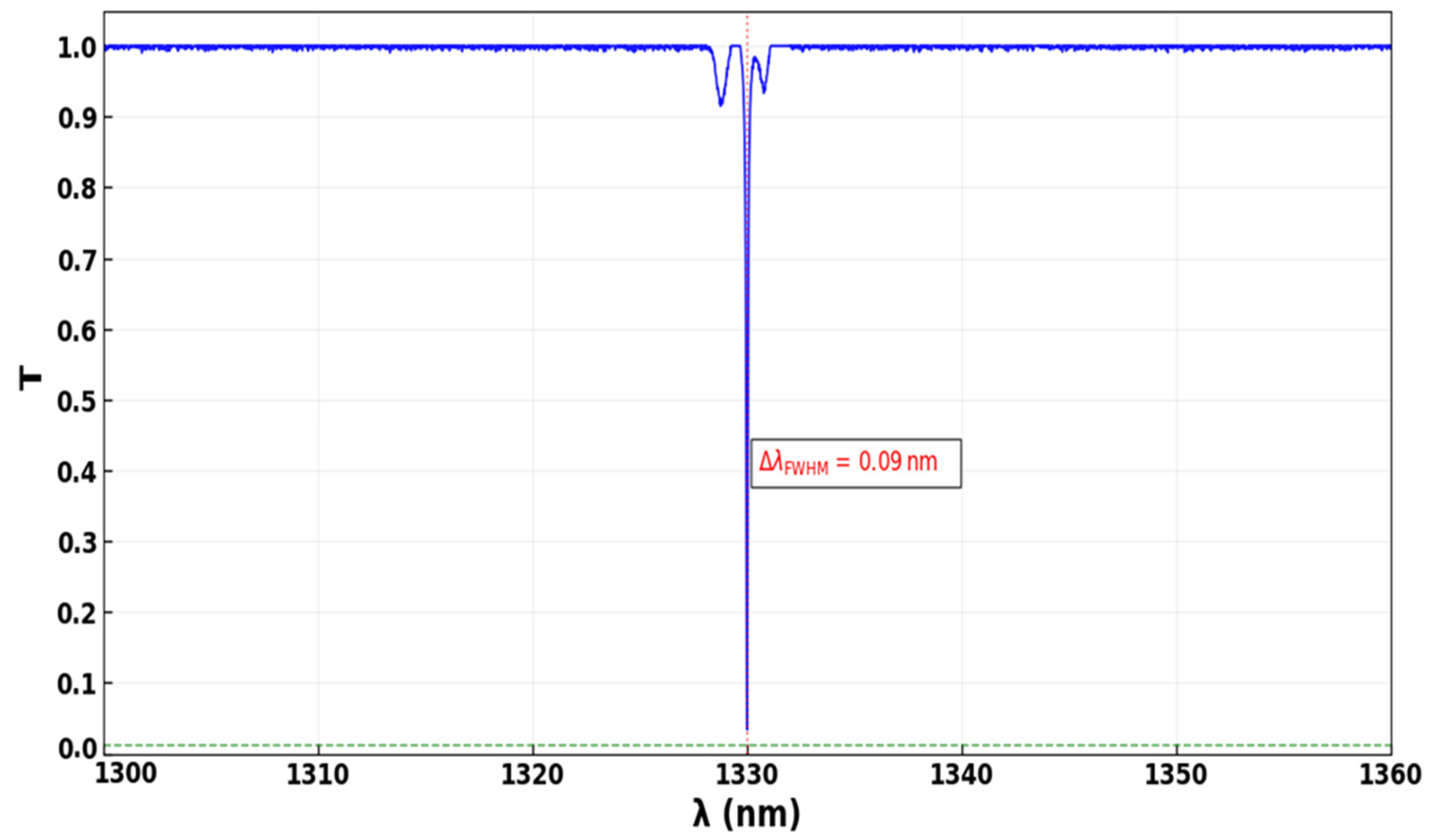
| XOR, AND, OR, NOT, NOR, XNOR, NAND | Silicon racetrack and ring resonator | Si/SiO2 | 7.24 × 1.5 | 47.94 | 1330 | CR = 13.09–14.67 | Sim. | This work |
Disclaimer/Publisher’s Note: The statements, opinions and data contained in all publications are solely those of the individual author(s) and contributor(s) and not of MDPI and/or the editor(s). MDPI and/or the editor(s) disclaim responsibility for any injury to people or property resulting from any ideas, methods, instructions or products referred to in the content. |
© 2025 by the authors. Licensee MDPI, Basel, Switzerland. This article is an open access article distributed under the terms and conditions of the Creative Commons Attribution (CC BY) license (https://creativecommons.org/licenses/by/4.0/).
Share and Cite
Kotb, A.; Wang, Z.; Zoiros, K.E. High-Performance All-Optical Logic Gates Based on Silicon Racetrack and Microring Resonators. Electronics 2025, 14, 2961. https://doi.org/10.3390/electronics14152961
Kotb A, Wang Z, Zoiros KE. High-Performance All-Optical Logic Gates Based on Silicon Racetrack and Microring Resonators. Electronics. 2025; 14(15):2961. https://doi.org/10.3390/electronics14152961
Chicago/Turabian StyleKotb, Amer, Zhiyang Wang, and Kyriakos E. Zoiros. 2025. "High-Performance All-Optical Logic Gates Based on Silicon Racetrack and Microring Resonators" Electronics 14, no. 15: 2961. https://doi.org/10.3390/electronics14152961
APA StyleKotb, A., Wang, Z., & Zoiros, K. E. (2025). High-Performance All-Optical Logic Gates Based on Silicon Racetrack and Microring Resonators. Electronics, 14(15), 2961. https://doi.org/10.3390/electronics14152961