Abstract
In the last decade, countries have experienced increased solar radiation, leading to an increase in the use of solar photovoltaic (PV) systems to boost renewable energy generation. However, the high solar penetration into these systems can disrupt the normal operation of the distribution grid. Thus, a major concern is the impact of these units on power quality indices. To improve these units, one approach is to design more efficient power inverters. This study introduces a pulse width modulation (PWM) technique for multilevel power inverters, employing a sine wave as the carrier wave and an amplitude over-modulated triangular wave as the modulator (PSTM-PWM). The proposed technique improves the waveform quality and increases the AC voltage output of the multilevel inverter compared with that from conventional PWM techniques. In addition, it ensures compliance with the EN50160 standard. These improvements are achieved with a lower modulation order than that used in traditional techniques, resulting in reduced losses in multilevel power inverters. The proposed approach is then implemented using a five-level cascaded H-bridge inverter. In addition, a comparative analysis of the efficiency of multilevel power inverters was performed, contrasting classical modulation techniques with the proposed approach for various modulation orders. The results demonstrate a significant improvement in both total harmonic distortion (THD) and power inverter efficiency.
1. Introduction
In recent years, the increasing reliance on fossil fuels and the continuous rise in their costs, alongside their detrimental environmental impact, have driven the development and implementation of alternative energy sources [1]. Among these sources, renewable energy plays a pivotal role, with PV solar energy emerging as one of the most rapidly expanding sectors [2,3]. However, the widespread integration of power electronic devices, such as power inverters employed in PV power plants, can significantly affect voltage levels and contribute to current distortion [4].
The selection of an appropriate inverter necessitates the consideration of several factors, including the power rating, efficiency, voltage range, current limitations, power factor, compatibility, cost, warranty provisions, local market certification, and harmonic distortion performance [5,6]. The optimal design of renewable energy grids, particularly in hybrid generation systems integrating photovoltaic and wind power, requires a balanced phase system and minimized harmonic content [7].
These technical challenges may restrict the capacity of the system to support additional PV integration if not adequately addressed. In networks where multiple small-scale PV installations are interconnected, grid quality can become a primary concern. At elevated penetration levels, the prevalence of power quality issues is expected to increase significantly [8]. Consequently, many countries have implemented stringent regulations regarding harmonic penetration from renewable energy sources, particularly photovoltaics, due to the high volume of distributed microgeneration [9].
In PV solar energy systems, solar radiation is converted into electrical energy by photovoltaic panels. These panels are widely adopted due to their clean, renewable nature and low maintenance requirements. To ensure efficient grid integration, power converters must be employed. These devices serve two key functions: First, they enable the solar panels to operate at their maximum power point (MPPT) [10,11,12]. Second, they convert the direct current (DC) generated by the panels into alternating current (AC) for grid feeding. Typically, two power conversion devices are utilized [13,14,15]. The first is a DC/DC converter, which facilitates operation at the maximum power point, while the second is a DC/AC converter that connects the PV system to the grid. The latter stage of energy conversion is conventionally achieved through the use of a three-phase voltage source inverter, either in a classical three-level or single-phase configuration [16,17,18]. However, alternative approaches have been proposed, with multilevel converter topologies representing a particularly promising option. These converters offer several advantages over conventional three-level inverters, including a reduced switching frequency, significantly lower output voltage distortion, and decreased dv/dt stress [19,20,21]. As a result, numerous multilevel power inverter topologies have been applied in PV systems [22,23].
Various configurations exist for photovoltaic systems [24]. The centralized configuration involves a single inverter that is responsible for converting the DC output from multiple panels into AC for grid integration. String technology connects panels sequentially, such that the electrical current generated by each panel is cumulatively added along the string. This configuration enhances the total voltage output, improving system efficiency and facilitating compliance with voltage requirements. Multi-string technology represents an advanced approach, integrating multiple strings of panels that are connected in both series and parallel configurations within a PV system. This methodology optimizes energy efficiency and system performance, particularly in large-scale installations. In a multi-string system, solar panels are arranged into distinct strings, each comprising several panels that are connected in serial connection. These strings are subsequently linked in parallel, leveraging the advantages of both configurations. The present work is oriented towards this latter configuration.
From a topological perspective, multilevel inverters can be categorized into three principal types: neutral point clamped (NPC), flying capacitor (FC), and cascaded H-bridge (CHB) multilevel inverters [25,26].
CHB multilevel converters are regarded as the most suitable topology for the next generation of PV plant converters due to their ability to operate with multiple independent low-voltage DC power supplies, which are readily available in PV systems [27,28,29]. These inverters consist of multiple H-bridge cells that are connected in series. Figure 1 illustrates a schematic of a cascaded H-bridge multilevel inverter integrating solar panels.
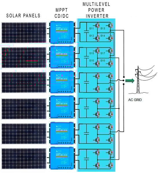
Figure 1.
Photovoltaic plant connected to a multilevel H-bridge inverter.
Each string of the PV array is interfaced with a DC/DC converter incorporating an MPPT algorithm. As multilevel inverters inherently generate higher output voltages than conventional three-level inverters, this topology presents a compelling solution for advanced PV power conversion systems.
Power inverters are non-linear elements that introduce harmonics into the electrical grid, potentially leading to temperature increases within the electrical system and a reduction in the residual lifespan of insulation [30]. In contemporary electrical distribution networks, there has been a significant rise in non-linear loads, including computers, fluorescent lighting, variable-speed electric motor drives, and power converters. These loads draw non-sinusoidal currents from the power grid, resulting in distortions in the sinusoidal current and voltage waveforms, commonly referred to as “harmonics” [31].
If the short-circuit power of the system is insufficient, these non-linear loads contribute to distortions in both current and voltage waveforms. Consequently, the waveforms deviate from their sinusoidal form and contain a certain number of harmonic components [31]. Since electrical system components are designed to operate under nominal frequency and standard conditions, the presence of harmonics induces several issues within the distribution network, including power losses, transformer and electrical machine overheating, increased neutral currents, erratic relay operation, and resonance phenomena.
Ensuring satisfactory power quality is a shared responsibility between the electricity supplier and the end user. According to the EN50160 standard [32], the supplier is the entity that is responsible for delivering electricity through a public distribution system, whereas the user is the customer who purchases electricity from the supplier. The user has the right to receive an adequate level of power quality from the supplier. In practice, power quality is determined by an agreement between both parties. The measurement and assessment of power quality should be conducted at the point of consumption. However, evaluating power quality is complex, as both the supplier and the user—whose sensitive electrical equipment may also generate disturbances—approach the issue from different perspectives. The EN50160 standard specifies the primary voltage parameters and their permissible deviation limits at the customer’s common coupling point within public low (LV) and medium (MV) voltage distribution networks under normal operating conditions. In this context, LV refers to a nominal phase-to-phase Root Mean Square (RMS) voltage not exceeding 1 kV, whereas MV encompasses nominal phase-to-phase RMS voltages ranging between 1 kV and 35 kV.
The EN50160 standard regulates the maximum permissible harmonic content that an electrical system can introduce into the grid. The standard specifies the percentage of each harmonic—both even and odd—as well as the maximum allowable waveform distortion, defined by the total harmonic distortion (THD) [33,34].
Multilevel inverters function by synthesizing a desired output voltage from multiple discrete DC voltage levels. As the number of input sources to a multilevel inverter increases, the resulting stepped waveform more closely approximates a sinusoidal output. Due to their low harmonic distortion and reduced switching requirements, multilevel inverters are highly suitable for DC/AC conversion applications. Its key features include the following:
- The ability to achieve higher output voltages with fewer switching devices compared with those from conventional inverters, where each switch only needs to block the voltage corresponding to a single DC level, mitigating the challenges associated with static and dynamic balancing in series-connected electronic devices.
- Increased inverter power capacity through higher voltage operation without needing an increase in current, thereby reducing conduction losses and enhancing inverter efficiency [35,36], where in this study, efficiency is defined as the minimization of power dissipation in inverter transistors relative to the delivered power.
- Finally, in multilevel inverters, the voltage THD levels, referred to in the EN50160 standard, remain approximately constant in the event of changes in the power delivered to the grid [37].
Power inverter control is achieved through pulse width modulation (PWM), a technique that can be adapted for multilevel inverters with certain modifications. For an N-level inverter, this strategy necessitates N-1 triangular carrier signals with identical frequencies and amplitudes. The fundamental concept involves comparing a sinusoidal reference wave with each carrier wave to generate the required switching pulses.
The control signals derived from the comparison of the modulator and carrier waves must meet specific criteria to preserve the symmetry of the waveforms as much as possible. The sine and triangular waveforms must be synchronized, starting symmetrically. To maintain an acceptable harmonic content, the carrier signal must have the highest possible frequency. However, as the carrier frequency increases, the switching frequency of the semiconductor devices also increases, which increases the thermal stress on the switching devices. This effectively limits the number of switches per cycle. The frequency modulation index is usually around 15 to achieve a standard-compliant THD level, which allows for commercial application. This study proposes a different approach using the PWM technique on a scale model to generate a modulated waveform with as reduced a modulation index as possible to, thus, comply with the EN50160 standard. It is implemented with only seven pulses per bridge in a five-level power inverter, whereas the alternative techniques compared require higher modulation rates to comply with the standard. The results are presented for modulation indices higher than 7, showing that the THD level is always lower in the proposed technique.
Section 2 presents the problem of classical PWM with respect to short-duration pulses that do not provide quality modulated waves, with modification to a discontinuous modulation proposed in the Proposed Phase Shift Triangle Modulator (PSTM) Technique subsection, which reduces the number of pulses and concentrates them in intervals with greater-slope modulator waves. The corresponding formulation and the results of the simulations in terms of THD and amplitude of the obtained modulated waveform are provided.
Section 3 shows the experimental implementation with a comparison between several classical techniques and the proposed techniques, showing oscillograms with the waveforms and the THD and amplitude levels of the modulated wave obtained in a multilevel inverter with nine-level (line-to-line) IGBT-type switches. The scale model implemented in the lab starts from the DC-Link voltages that would appear in a typical string of a PV array. All of these voltages feed the multilevel power inverter so that the three-phase AC output voltage will be applied to a three-phase load.
Section 4 presents a discussion of the results and summarizes the most relevant conclusions.
2. PWM Techniques
Figure 2 illustrates a sinusoidal PWM signal, demonstrating that, as the instantaneous value of the modulator (sinusoidal) wave increases, the instantaneous switching frequency of the transistors also rises. Consequently, the number of pulses per cycle must be reduced to prevent overheating of the circuit breakers. Unwanted harmonic content emerges at the carrier frequency, with sidebands diminishing in amplitude as they move away from the carrier frequency.
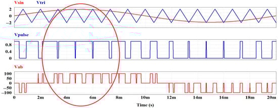
Figure 2.
PWM signals. Vsin, Vtri, Vpulse, Vab: modulator, carrier, modulated, and output waves.
If the number of cycles is low, the first unwanted harmonics will occur at lower frequencies. Therefore, it is advisable to maximize the number of cycles to ensure that unwanted harmonics are shifted to higher frequencies. Additionally, as the carrier frequency increases and the instantaneous value of the modulator wave approaches the carrier frequency, the switching frequency of the transistors also increases.
Ideally, modulation should be minimized or eliminated in the region where the modulator and carrier values coincide. This would prevent excessive switching, thereby maintaining a consistent number of pulses per period. In this context, achieving an optimal balance between modulation order and carrier frequency is crucial. A higher modulation order elevates the frequency of the first unwanted harmonics, considering that the EN50160 standard only applies up to the 25th harmonic. However, an increased carrier frequency also leads to higher transistor switching activity, thereby exacerbating switching losses.
The technical literature presents several conventional PWM control methods for multilevel inverters, including amplitude shift PWM (LS-PWM) [38], phase shift PWM (PS-PWM) [39], and harmonic injection phase shift PWM (HPS-PWM) techniques. This paper presents the PSTM-PWM technique to improve these techniques both in terms of inverter output quality and efficiency.
On the other hand, the reliability and lifespan of power semiconductors are critical parameters for assessing power electronic systems, particularly in renewable energy generation, electric vehicles, and aerospace applications [40]. These sectors operate in harsh environmental conditions, which can induce thermo-mechanical stress, leading to wear, ageing, and degradation.
Calculating losses in a multilevel inverter is a complex task, significantly more challenging than in conventional two-level inverters. This complexity arises due to the varying current distribution across different power switches. Several methods have been proposed in the literature to evaluate power loss in multilevel inverters. Some approaches rely on online calculations from simulated circuits, while others are based on detailed mathematical analyses and computations [41]. A purely experimental approach, as proposed in this study, involves measuring the continuous power input and the active power output from the H-bridges. These measurements will be conducted using both the proposed and conventional techniques for various modulation orders (M). For this evaluation, a fundamental harmonic RMS voltage of 220 V was used uniformly across all techniques.
Power losses (PCT) in semiconductor components can be categorized into three types: conduction losses (Pc), switching losses (Psw), and blocking losses (Pb), the latter of which is typically negligible [42]:
Proposed Phase Shift Triangle Modulator (PSTM) Technique
The Proposed Phase Shift Triangle Modulator (PSTM) technique is a specialized form of pulse width modulation (PWM) that differs from conventional approaches by using a sinusoidal waveform as the carrier signal and a triangular waveform as the modulator signal—effectively inverting the traditional PWM structure.
In this modulation scheme, the triangular wave possesses a peak amplitude that exceeds that of the sinusoidal carrier. This configuration has a significant impact on the system’s switching behavior. Specifically, as the peak value of the triangular modulator increases, there are extended intervals during which the triangular wave does not intersect the sinusoidal carrier. These non-intersecting periods correspond to segments of the waveform where no modulation—and thus no switching—occurs.
This phenomenon results in what is known as an over-modulated signal, characterized by long sections of constant output (flat-top or flat-bottom waveforms), which deviate from the ideal PWM shape. While this can help reduce the number of switching transitions and, therefore, lower switching losses, it can also introduce waveform distortion and affect output fidelity if not properly managed.
To mitigate the undesirable side effects of over-modulation and to preserve a consistent number of switching events per period, it is essential to dynamically adjust the carrier frequency (fp) in response to variations in the modulator’s peak amplitude (triangular wave). By doing so, the system maintains a constant effective modulation order, denoted as M, which is defined by the ratio (M = fp/fm), where fm is the frequency of the triangular modulator waveform.
Maintaining a constant modulation index M ensures that the system’s switching behavior remains predictable and that the harmonic profile of the output does not deteriorate due to inconsistent modulation.
Figure 3 illustrates this principle, showing how varying the peak of the triangular modulator while compensating through adjustments in the carrier frequency allows the PSTM method to retain a stable modulation order and prevent excessive signal distortion. This balance is crucial for achieving both high efficiency and acceptable output quality in power electronic applications.
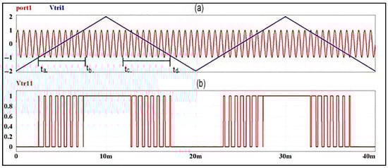
Figure 3.
PSTM technique: (a) carrier and modulator waves and (b) modulated waves for M = 15.
To obtain the carrier frequency, the sine wave carrier is compared with the half-period of a triangular modulator waveform, which gives us the equation of a value line:
where V is the peak value of the modulator wave. The modulation will only occur for t, with t = tb − ta, if the maximum value of the sine is 1; then,
where ta is the beginning of modulation in the first half-period of the modulated wave and tb is the instant when modulation ends. Likewise, tc and td are for the second half-period.
Then, the period during which the modulation lasts (subtracting tb from ta) is
Between ωmta and ωmtb, M/2 switches must be present (where M is the actual modulation order), and between ωmtc and ωmtd, other M/2 switches must be present. The carrier frequency can be calculated by knowing how many pulses must be present in half a period of the modulator, i.e., how many pulses are in π. The total number of pulses in half a period is, therefore,
The number of pulses in 2 π radians is doubled:
Using Equations (5) and (6), we obtain
where Mt is the theoretical modulation order because the modulation is discontinuous. This indicates that the carrier will have to have a pulsation MV times that of the modulator wave:
As an example, the carrier frequency for a modulation order of 15 pulses, a peak voltage of 2 V for a triangular signal, a 1 V peak voltage for the modulator signal and a frequency of 50 Hz should be 1500 Hz.
As mentioned above, increasing the number of switchovers per period heats the circuit breakers and decreases the efficiency of the inverter. It is, therefore, desirable to work with as low a modulation order M as possible. For the PSTM-PWM technique, a modulation order M = 7 has been chosen, which complies with the EN50160 standard. Furthermore, the choice of M = 7 implies that the switching losses are lower and, therefore, the efficiency of the multilevel power inverter higher, as shown in the experimental results.
To determine which peak values are the most suitable for the intended purpose, i.e., low THD and high RMS values for the fundamental voltage, a sweep of the peak voltage of the triangular modulator was carried out to determine which value reduces the THD by the most and has the highest RMS of the fundamental voltage, all this with a modulation order of M that equals 7.
Figure 4a shows the THD value as a function of the peak value of the triangular modulator with a real modulation order M of 7. The maximum value of the carrier was kept at 1 V. Minimum THD values were obtained for modulator peak voltages of 1.4 V and 3.5 V. Figure 4b shows how the RMS value of the fundamental term varies as a function of the modulator peak voltage. Additionally, with a sinusoidal carrier voltage of 1 V, for the 3.5 V peak voltage, we obtain a higher RMS value for the fundamental voltage.
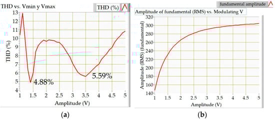
Figure 4.
(a) THD versus modulator waveform peak voltage. (b) Amplitude of fundamental versus modulator waveform peak voltage.
3. Experimental Investigation of the Proposal
To contrast the simulations, a scale model was assembled in the laboratory, in which the following blocks were used:
To emulate the photovoltaic panels, a 100 V DC-Link was used, as a total of 24 panels were required. For the multilevel inverter, six H-bridges were mounted. The control consisted of a PC with a National Instruments™ (Austin, TX, USA) card. In addition, a variable resistive load was employed to accurately measure the THD value of the waveform to be fed into the grid. The different modules are detailed below in Figure 5.
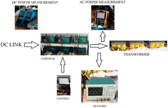
Figure 5.
Experimental model. Control, multilevel inverters, transformers, and measurement equipment.
The H-bridge was assembled using GPT-IGBT (GUASCHS™, Barcelona, Spain) modules. This module enables the construction of an H-bridge using insulated gate bipolar transistors IGBTs LUH100G1204 (SEMIKRON™, Munich, Germany) 1200 V, 100 A, a rise time (tr) of 60 ns, and a fall time (tf) of 200 ns for a DC-Link voltage of 600 V. It incorporates a three-phase bridge rectifier, a capacitor bank, IGBTs with a forced air-cooled heat sink, opto-coupled drivers, output phase current sensors, a DC-Link current sensor, and a DC-Link voltage sensor. The primary electrical specifications are as follows: the maximum voltage applied to the DC-Link is 750 V, and the maximum output current per phase is 32 A. The technical data of ISF-245 panels were used [43].
National Instruments hardware, specifically the NI9154 card, was employed to generate control signals for the inverter stages. A LabVIEW™ (2020 version, Austin TX, USA)-based platform was developed to facilitate the implementation of various PWM techniques. Voltage harmonics at the inverter output were measured using three-phase power analyzers, while power quality was evaluated using a C.A 8336 (Chauvin ArnouxTM Asnières-sur-Seine, France) capable of measuring the first 50 harmonics. The DC supply voltage (Uc) powering the H-bridges was 100 V.
Experimental Investigation of the Proposed Phase Shift Triangle Modulator (PSTM) Technique
The control waveform for the power transistors was generated by comparing the modulator signals, which have a 120-degree phase shift, with the carrier signals, which exhibit a 90-degree phase shift. The modulators operated within a three-phase system, with each modulator being phase-shifted by 120 degrees relative to the others. Similarly, the sinusoidal carrier signals were also phase-shifted but, in this case, by 90 degrees. This phase relationship between the modulator and carrier signals is crucial for achieving precise and efficient modulation. To prevent the introduction of second-order harmonics, the waveforms must be symmetrical with respect to one-quarter of a period.
Figure 6a illustrates the comparison between the triangular modulator waveform and the sinusoidal carrier signals for a multilevel H-bridge inverter. The figure demonstrates that the triangular modulator waveform attains a peak value of 1.4 V. This comparison process is fundamental for generating accurate control signals, which are subsequently applied to the gate terminals of the IGBT transistors.
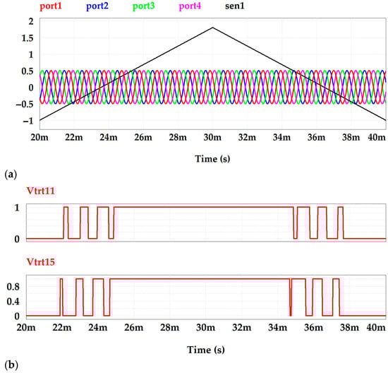
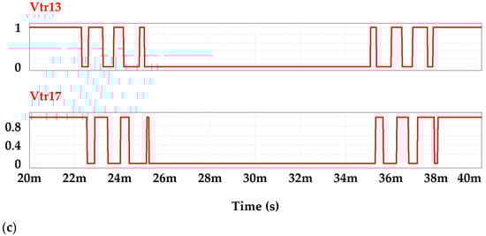
Figure 6.
(a) Carriers and modulator waves for multilevel inverters. (b,c) Generated control signals.
The control signals generated through this modulation approach are depicted in Figure 6b.
Figure 7 presents the relationship between the control signals and one of the phases corresponding to two H-bridges, which is directly correlated with Figure 6b. These signals—Vtr11, Vtr13, Vtr15, and Vtr17—controlled transistors S11, S13, S15, and S17, respectively. Furthermore, transistors S12, S14, S16, and S18 were driven by the inverted versions of Vtr11, Vtr13, Vtr15, and Vtr17. The remaining two phases were generated in a similar manner, employing triangular modulators that were phase-shifted by 120 and 240 degrees, respectively. Figure 7b shows the input signals Vtr11 and Vtr13 attacking the IGBT transistors S11 and S13 with an offset of 270º using the technique PSTM-PWM V = 1.4. The 90º phase shift occurred in the sequential order of S11, S15, S17, and S13. As can be seen, the shortest pulse duration applied to the IGBTs transistor was 0.24 ms—Figure 7b—compared to the tr and tf times; the smaller pulse width was an order of magnitude three times larger.
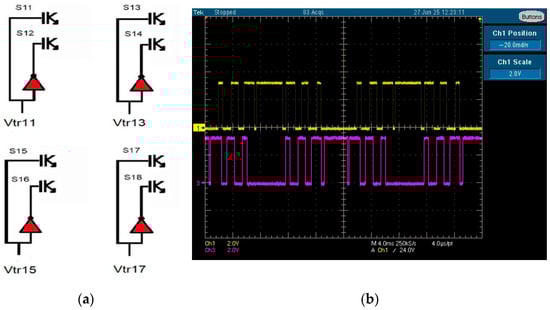
Figure 7.
(a) Distribution of control signals on a phase. (b) Vtr11 and Vtr13 input signals to IGBT transistors M = 7 PSTM-PWM V = 1.4.
Figure 8 shows the maximum permissible amplitudes of the harmonics corresponding to the EN50160 standard in percent. Figure 9 shows the oscillograms and spectra of the classical PWM techniques: Figure 9a,b, LS-PWM; Figure 9c,d, PS-PWM; and Figure 9e,f, PS-PWMHI. Figure 10 shows the oscillograms and spectra of the proposed PWM technique for two V values: Figure 10a,b, PSTM-PWM, V = 1.4; Figure 10c,d, PSTM-PWM, V = 3.5. For a comparison of the techniques, the same modulation order M = 7 and a supply voltage of 100 V DC were used. To measure the line-to-line voltage of the three-phase system, a probe (Mark) with a gain of ×200 was used. The experiment was carried out at an ambient temperature of 25 °C, with 15 measurements of voltage and power for each technique implemented, of which the arithmetic mean value was used for comparison.
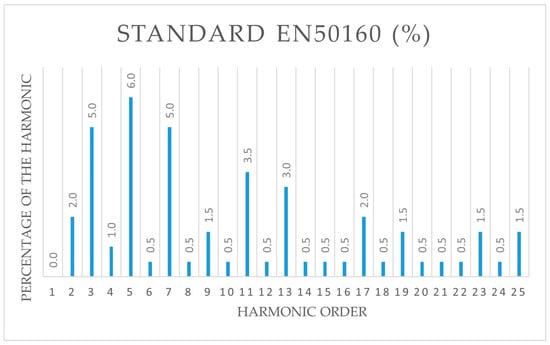
Figure 8.
Maximum harmonic amplitudes permitted by the EN50160 standard in percentages.
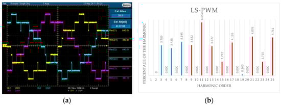
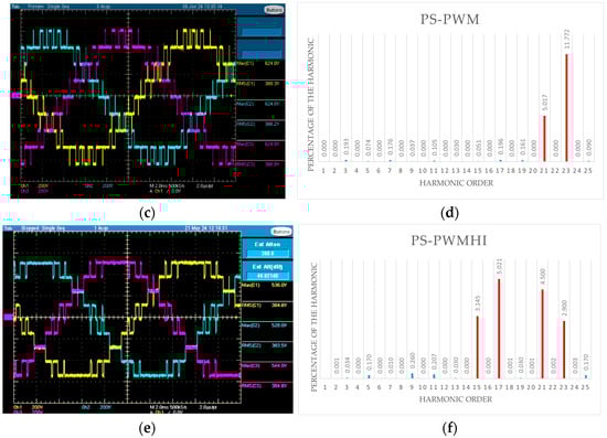
Figure 9.
Oscillograms and spectra of classical PWM techniques: (a,b) LS-PWM; (c,d) PS-PWM; (e,f) PS-PWMHI.
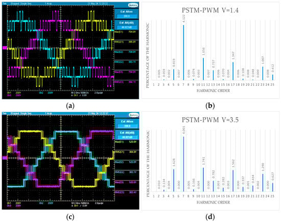
Figure 10.
Oscillograms and spectra of the proposed PWM technique: (a,b) PSTM-PWM, V = 1.4; (c,d) PSTM-PWM, V = 3.5.
In the spectra, the harmonics that do not comply with the EN50160 standard are shown in red. The proposed techniques were found to comply with this standard better than the classical techniques, which contain harmonics that do not comply with the standard.
Figure 11 shows the THD of these techniques, where those that do not comply with the admissible THD of the EN50160 standard are shown in red. In the aforementioned comparison conditions, the proposed technique already complies with the requirements established by the EN50160 standard, while the others do not comply because the harmonic values exceed the maximum limits allowed by the standard.
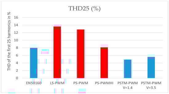
Figure 11.
THD of the first 25 harmonics for each PWM technique.
As a resume, Table 1 presents the values of the harmonics of the techniques that do not comply with the aforementioned standard, as well as the different THD.

Table 1.
Harmonic terms (%) non-compliant with EN50160 for different modulation techniques with multilevel inverter and M = 7. Values in red do not meet the standard.
In summary, the presented figures provide a comprehensive analysis of the derivation of control signals for this modulation technique and their correlation with the output voltages. This technique was compared with traditional modulation methods used in H-bridge multilevel inverters, including amplitude shift modulation (LS-PWM), phase shift modulation (PS-PWM), and phase shift modulation with harmonic injection (HPS-PWM). The results correspond to a modulation order of M = 7 and a DC supply voltage of Uc = 100 V. Under these conditions, the proposed technique already meets the requirements set by the EN50160 standard, whereas the other methods fail to comply due to harmonic values exceeding the maximum limits allowed by the standard. Additionally, it should be noted that none of the three conventional techniques satisfy the total harmonic distortion (THD) factor required by the standard.
Moreover, when a peak voltage of 3.5 V is applied in the modulator, the RMS value of the fundamental voltage increases by 5% compared with that of the best conventional technique: PS-PWM with harmonic injection, as shown in Figure 12. Although this classical method is the closest to compliance with the standard, the proposed technique outperforms it in both signal quality and voltage amplitude.
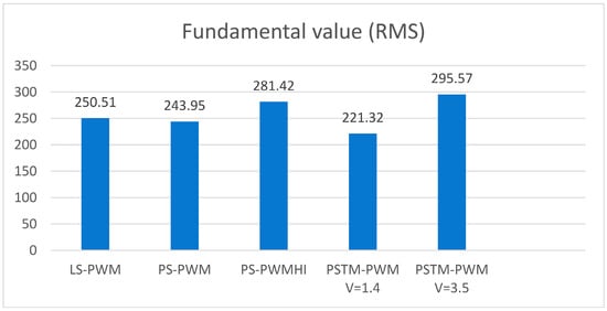
Figure 12.
Fundamental value (RMS) for each PWM technique.
This increase in RMS value of the fundamental voltage is particularly important, as it enhances power conversion efficiency, minimizing losses and improving the overall performance of the multilevel inverter. The ability of the proposed technique to reduce harmonics to acceptable levels without requiring additional filters, along with its improved THD, underscores its potential as a more efficient and optimized solution for integrating PV plants into the grid, as the most suitable implementation.
In summary, the proposed modulation technique not only complies with the EN50160 standard for a modulation order of M = 7 but also offers significant improvements in signal quality and achieves a higher RMS line voltage at the same DC voltage.
In this study, the power inverter efficiency of classical modulation techniques is compared with that of the PSTM technique. Figure 13 illustrates the multilevel power inverter efficiency curves of five modulation methods as a function of modulation order. From the graph, it is evident that, as the number of switching events increases, the switching losses also increase. This trend suggests that, for a modulation order of M = 7, all techniques have lower losses than those with higher M values. For the same M, techniques with lower THD and, consequently, lower harmonic content relative to the RMS value, have lower conduction losses.
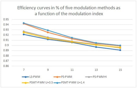
Figure 13.
Power inverter efficiency curves for different modulation techniques.
The PSTM-PWM technique for V = 1.4 outperforms the other methods. Additionally, while efficiency decreases at higher modulation indices, it remains superior to other techniques for the same M value. To obtain the efficiency of the multilevel power inverter for the different techniques, the DC power at the input of each H-bridge was applied at constant voltage for all techniques. The three-phase alternating current power at the output of the inverter was measured with the same applied load. The relationship between the two is shown in the figure below.
4. Discussion and Conclusions
The rapid expansion of multilevel inverters within the photovoltaic sector has significantly transformed the energy industry. These devices, leveraging advanced modulation techniques, enhance the efficiency of solar energy conversion into usable electricity. However, this advancement is accompanied by challenges, particularly regarding the generation of harmonics injected into the power grid, which poses concerns about the quality of the power supply.
In this regard, the EN50160 standard serves as a critical benchmark. This standard defines the power quality parameters that electrical supply systems must adhere to, including permissible harmonic levels. Compliance with the EN50160 standard is essential for multilevel inverters, as it ensures reliability and stability of power systems while facilitating the seamless integration of photovoltaic (PV) systems into the grid.
The experimental equipment consists of a multilevel inverter with cascade H-bridge configuration. One of the characteristics of this inverter is that it requires independent DC sources in each H-bridge. However, in large photovoltaic plants, this would not be a problem because each array would be connected to a different H-bridge, so the proposal presented is very suitable for photovoltaic systems.
Moreover, other digital SPWM controllers are also widely used, the multilevel inverter was chosen so that both the modulation technique and modulation order can be modified.
To achieve compliance with the standard without the need for output waveform filtering for harmonic reduction, a novel modulation approach was proposed for multilevel inverters intended for grid-connected PV plants. This technique was benchmarked against conventional modulation strategies to assess its effectiveness. The results demonstrate that the proposed technique meets the EN50106 standard for a modulation order of M = 7, whereas the conventional techniques fail to do so.
Regarding inverter efficiency, for all applied frequency modulation orders, the proposed technique was observed to outperform traditional approaches, achieving standard compliance at M = 7 and resulting in a higher efficiency for the multilevel inverter compared with alternative modulation methods. With a peak voltage of 1.4 V in the modulator waveform, the proposed technique achieved the lowest total harmonic distortion (THD) of 4.89%, representing an almost 50% reduction compared with the best conventional technique. Furthermore, when a peak voltage of 3.5 V was applied to the modulator, the RMS value of the fundamental voltage increased by 5% relative to the best conventional technique (PS-PWM with harmonic injection). Although this classical technique comes closest to meeting the standard, the proposed method surpasses it in both efficiency and RMS line voltage output per unit of DC input voltage applied to the inverter.
Finally, although the article describes the application being used without a transformer at the inverter output, the proposed technique is also fully applicable in systems that include a transformer at the output. By adding inductors before and after the transformer, it is possible to smooth the two-level commutation produced by this method, resulting in a true sine wave at the output, for which only a capacitor needs to be added. This capability makes it suitable for powering appliances such as refrigerators, which is a relevant point worth mentioning.
In addition to direct connection to the grid of photovoltaic systems, with or without transformers, this modulation technique could be applied to drive electric motors or isolated AC loads.
Author Contributions
Conceptualization, F.M.P.-H. and J.-R.H.-L.; methodology, F.M.P.-H. and A.R.-G.; software, A.R.-G. and M.J.M.-G.; hardware, F.M.P.-H., J.-R.H.-L. and A.R.-G.; data curation, A.R.-G. and M.J.M.-G.; writing—original draft preparation, F.M.P.-H. and J.-R.H.-L.; writing—review and editing, A.R.-G. and M.J.M.-G. All authors have read and agreed to the published version of the manuscript.
Funding
This research received no external funding.
Data Availability Statement
The data are contained in this paper.
Acknowledgments
During the preparation of this manuscript/study, the authors used ChatGPT (GPT-4.5) to improve the English text. The authors have reviewed and edited the output and take full responsibility for the content of this publication.
Conflicts of Interest
The authors declare no conflict of interest.
References
- Soto, E.A.; Wollega, E.; Ortega, A.V.; Hernandez-Guzman, A.; Bosman, L. Reduction in Emissions by Massive Solar Plant Integration in the US Power Grid. Energies 2024, 17, 1611. [Google Scholar] [CrossRef]
- Nayak, P.K.; Mahesh, S.; Snaith, H.J.; Cahen, D. Photovoltaic solar cell technologies: Analysing the state of the art. Nat. Rev. Mater. 2019, 4, 269–285. [Google Scholar] [CrossRef]
- Heidari, M.R.; Heravi, G. Development of flexible supportive policy with real options for renewable energy projects: Case of photovoltaic systems. Renew. Energy 2024, 225, 120326. [Google Scholar] [CrossRef]
- Li, S.; Zhou, S.; Li, H. Harmonic Suppression Strategy of LCL Grid-Connected PV Inverter Based on Adaptive QPR_PC Control. Electronics 2023, 12, 2282. [Google Scholar] [CrossRef]
- IEEE Standard 1250-2011; IEEE Guide for Identifying and Improving Voltage Quality in Power Systems. IEEE Power & Energy Society: Piscataway, MJ, USA, 2011.
- Yan, X.; Huang, S.; Li, R.; Jia, J.; Han, L.; Dong, X. Harmonic voltage compensation and harmonic current sharing strategy of grid-forming inverter. Electr. Power Syst. Res. 2025, 238, 111115. [Google Scholar] [CrossRef]
- Iqbal, H.; Sarwat, A. Design and Implementation of Hybrid GA-PSO-Based Harmonic Mitigation Technique for Modified Packed U-Cell Inverters. Energies 2024, 18, 124. [Google Scholar] [CrossRef]
- Shahin, M.; Topriska, E.; Gormley, M.; Nour, M. Design and field implementation of smart grid-integrated control of PV inverters for autonomous voltage regulation and VAR ancillary services. Electr. Power Syst. Res. 2022, 208, 107862. [Google Scholar] [CrossRef]
- Rai, I.; Sucheta, C. Microgrid and grid synchronization: A critical analysis of challenges and opportunities. Electr. Power Syst. Res. 2025, 242, 111434. [Google Scholar] [CrossRef]
- Kolodziejski, W.; Jasielski, J.; Machowski, W.; Godek, J.; Szerszeń, G. Single-Phase Transformerless Three-Level PV Inverter in CHB Configuration. Electronics 2025, 14, 364. [Google Scholar] [CrossRef]
- Khalid, W.; Awais, Q.; Jamil, M.; Khan, A.A. Dynamic Simulation and Optimization of Off-Grid Hybrid Power Systems for Sustainable Rural Development. Electronics 2024, 13, 2487. [Google Scholar] [CrossRef]
- Asif; Ahmad, W.; Qureshi, M.B.; Khan, M.M.; Fayyaz, M.A.B.; Nawaz, R. Optimizing large-scale PV systems with machine learning: A neuro-fuzzy MPPT control for PSCs with uncertainties. Electronics 2023, 12, 1720. [Google Scholar] [CrossRef]
- Ahangarkolaei, J.M.; Izadi, M.; Nouri, T. Applying a sliding mode controller to maximum power point tracking in a quasi z-source inverter based on the power curve of a photovoltaic cell. Electronics 2022, 11, 2164. [Google Scholar] [CrossRef]
- Kadhim, I.J.; Hasan, M.J. Enhancing power stability and efficiency with multilevel inverter technology based on renewable energy sources. Electr. Power Syst. Res. 2024, 231, 110290. [Google Scholar] [CrossRef]
- Zhang, T.; Jiang, J.; Chen, D. An efficient and low-cost DMPPT approach for photovoltaic submodule based on multi-port DC converter. Renew. Energy 2021, 178, 1144–1155. [Google Scholar] [CrossRef]
- Mali, R.; Adam, N.; Satpaise, A.; Vaidya, A.P. Performance Comparison of Two Level Inverter with Classical Multilevel Inverter Topologies. In Proceedings of the 2019 IEEE International Conference on Electrical, Computer and Communication Technologies (ICECCT), Coimbatore, India, 20–22 February 2019. [Google Scholar] [CrossRef]
- Cho, Y. Dual-buck residential photovoltaic inverter with a high-accuracy repetitive current controller. Renew. Energy 2017, 101, 168–181. [Google Scholar] [CrossRef]
- He, F.; Zhao, Z.; Yuan, L. Impact of inverter configuration on energy cost of grid-connected photovoltaic systems. Renew. Energy 2012, 41, 328–335. [Google Scholar] [CrossRef]
- Choudhury, S.; Bajaj, M.; Dash, T.; Kamel, S.; Jurado, F. Multilevel Inverter: A Survey on Classical and Advanced Topologies, Control Schemes, Applications to Power System and Future Prospects. Energies 2021, 14, 5773. [Google Scholar] [CrossRef]
- Antonio-Ferreira, A.; Collados-Rodríguez, C.; Gomis-Bellmunt, O. Modulation techniques applied to medium voltage modular multilevel converters for renewable energy integration: A review. Electr. Power Syst. Res. 2018, 155, 21–39. [Google Scholar] [CrossRef]
- Amamra, S.A.; Meghriche, K.; Cherifi, A.; Francois, B. Multilevel Inverter Topology for Renewable Energy Grid Integration. IEEE Trans. Ind. Electron. 2017, 64, 8855–8866. [Google Scholar] [CrossRef]
- Omer, P.; Kumar, J.; Surjan, B.S. A Review on Reduced Switch Count Multilevel Inverter Topologies. IEEE Access 2020, 8, 22281–22302. [Google Scholar] [CrossRef]
- Yu, Y.; Konstantinou, G.; Hredzak, B.; Agelidis, V.G. Power Balance of Cascaded H-Bridge Multilevel Converters for Large-Scale Photovoltaic Integration. IEEE Trans. Power Electron. 2016, 31, 292–303. [Google Scholar] [CrossRef]
- Belhachat, F.; Larbes, C. Modeling, analysis and comparison of solar photovoltaic array configurations under partial shading conditions. Sol. Energy 2015, 120, 399–418. [Google Scholar] [CrossRef]
- Aslam, A.W.; Hassan, J.; Minambres-Marcos, V.; Al-Salloomee, A.G.S.; Roncero-Clemente, C. Traditional and Hybrid Topologies for Single-/Three-Phase Transformerless Multilevel Inverters. Electronics 2024, 13, 4058. [Google Scholar] [CrossRef]
- Nyamathulla, S.; Chittathuru, D.; Muyeen, S.M. An overview of multilevel inverters lifetime assessment for grid-connected solar photovoltaic applications. Electronics 2023, 12, 1944. [Google Scholar] [CrossRef]
- Fernão Pires, V.; Martins, J.F.; Foito, D.; Hão, C. A Grid Connected Photovoltaic System with a Multilevel Inverter and a Le-Blanc Transformer. Int. J. Renew. Energy Res. 2012, 2, 84–91. [Google Scholar] [CrossRef]
- Babei, E.; Laali, S.; Alilu, S. Cascaded multilevel inverter with series connection of novel H-bridge basic units. IEEE Trans. Ind. Electron. 2014, 61, 6664–6671. [Google Scholar] [CrossRef]
- Sastry, J.; Bakas, P.; Kim, H.; Wang, L.; Marinopoulos, A. Evaluation of cascaded H-bridge inverter for utility-scale photovoltaic systems. Renew. Energy 2014, 69, 208–218. [Google Scholar] [CrossRef]
- Dudek, J.; Chlebis, P. Comparison of power losses and quality of output voltage from different types of inverters. In Proceedings of the IEEE 35th Annual Power Electronics Specialists Conference (IEEE Cat. No. 04CH37551), Aachen, Germany, 20–25 June 2004; Volume 4, pp. 3120–3126. [Google Scholar] [CrossRef]
- Lago, J.; Felipe, F.N.; Dupczak, B.S. Three-phase photovoltaic inverter control strategy for low voltage grid current unbalance mitigation. Electr. Power Syst. Res. 2023, 225, 109879. [Google Scholar] [CrossRef]
- DIN EN50160; Voltage Characteristics of Electricity Supplied by Public Distribution Networks. DIN: German Institute for Standardization: Berlin, Germany, 2025.
- Bayer, B.; Matschoss, P.; Thomas, H.; Marian, A. The German experience with integrating photovoltaic systems into the low-voltage grids. Renew. Energy 2018, 119, 129–141. [Google Scholar] [CrossRef]
- Guerrero-Perez, J.; De Jodar, E.; Gómez-Lázaro, E.; Molina-Garcia, A. Behavioral modeling of grid-connected photovoltaic inverters: Development and assessment. Renew. Energy 2014, 68, 686–696. [Google Scholar] [CrossRef]
- Boonmee, C.; Somboonkit, P.; Watjanatepin, N. Performance comparison of three-level and multi-level for Grid-connected photovoltaic systems. In Proceedings of the 12th International Conference on Electrical Engineering/Electronics, Computer, Telecommunications and Information Technology (ECTI-CON), Hua Hin, Thailand, 24–27 June 2015; pp. 1–5. [Google Scholar] [CrossRef]
- Mohamad, A.S.; Mariun, N. Simulation analysis of an improved cascaded multilevel inverter topology. In Proceedings of the IEEE International Conference on Power and Energy (PECon), Melaka, Malaysia, 28–30 November 2016; pp. 178–181. [Google Scholar] [CrossRef]
- Agrawal, R.; Jain, S. Multilevel inverter for interfacing renewable energy sources with low/medium- and high-voltage grids. IET Renew. Power Gener. 2017, 11, 1822–1831. [Google Scholar] [CrossRef]
- Angulo, M.; Lezana, P.; Kouro, S.; Rodriguez, J.; Wu, B. Level-shifted PWM for cascaded multilevel inverters with even power distribution. In Proceedings of the IEEE 38th Annual Power Electronics Specialists Conference, Orlando, FL, USA, 17–21 June 2007; pp. 2373–2378. [Google Scholar] [CrossRef]
- Darus, R.; Konstantinou, G.; Pou, J.; Ceballos, S.; Agelidis, V.G. Comparison of phase-shifted and level-shifted PWM in the modular multilevel converter. In Proceedings of the 7th International Power Electronics Conference, Hiroshima, Japan, 18–21 May 2014; pp. 3764–3770. [Google Scholar] [CrossRef]
- Yu, X.; Zhou, D.; Iannuzzo, F. Comparative Analysis of Power Semiconductor Thermal Stress in DC and AC Power Cycling. In Proceedings of the IEEE 13th International Symposium on Power Electronics for Distributed Generation Systems (PEDG), Kiel, Germany, 26–29 June 2022; pp. 1–6. [Google Scholar] [CrossRef]
- Alamri, B.; Alshahrani, S.; Darwish, M. Losses investigation in SPWM-controlled cascaded H-bridge multilevel inverters. In Proceedings of the 2015 50th International Universities Power Engineering Conference (UPEC), Stoke-on-Trent, UK, 1–4 September 2015; pp. 1–5. [Google Scholar] [CrossRef]
- Guo, X.; Wang, X.; Wang, C.; Lu, Z.; Hua, C.; Blaabjerg, F. Improved Modulation Strategy for Singe-Phase Cascaded H-Bridge Multilevel Inverter. IEEE Trans. Power Electron. 2022, 37, 2470–2474. [Google Scholar] [CrossRef]
- Sánchez-Pacheco, F.J.; Sotorrío-Ruiz, P.J.; Heredia-Larrubia, J.R.; Pérez-Hidalgo, F.; De Cardona, M. PLC-Based PV Plants Smart Monitoring System: Field Measurements and Uncertainty Estimation. IEEE Trans. Instrum. Meas. 2014, 63, 2215–2222. [Google Scholar] [CrossRef]
Disclaimer/Publisher’s Note: The statements, opinions and data contained in all publications are solely those of the individual author(s) and contributor(s) and not of MDPI and/or the editor(s). MDPI and/or the editor(s) disclaim responsibility for any injury to people or property resulting from any ideas, methods, instructions or products referred to in the content. |
© 2025 by the authors. Licensee MDPI, Basel, Switzerland. This article is an open access article distributed under the terms and conditions of the Creative Commons Attribution (CC BY) license (https://creativecommons.org/licenses/by/4.0/).