
High-Gain Coupled-Inductor Boost Converters Using Voltage-Doubling and Continuous Input Current Design


Abstract
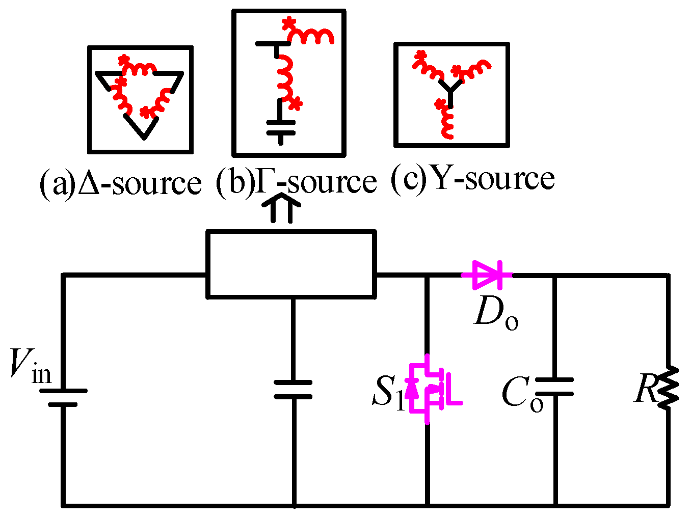
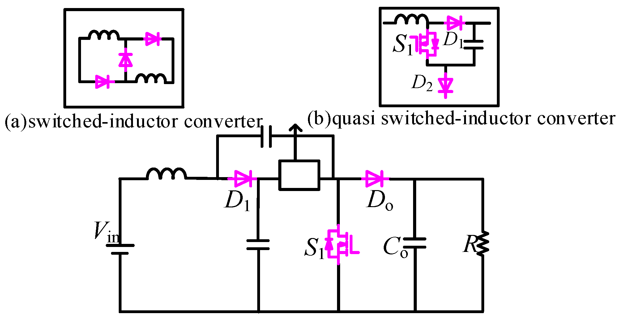
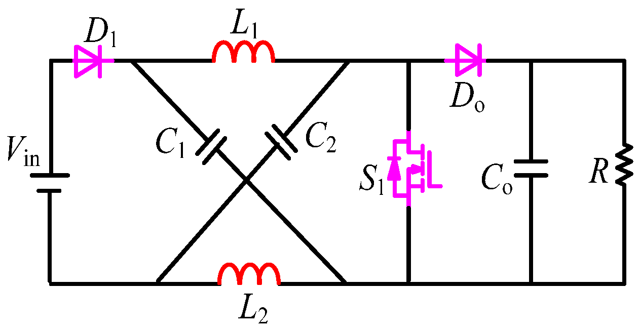
1. Introduction
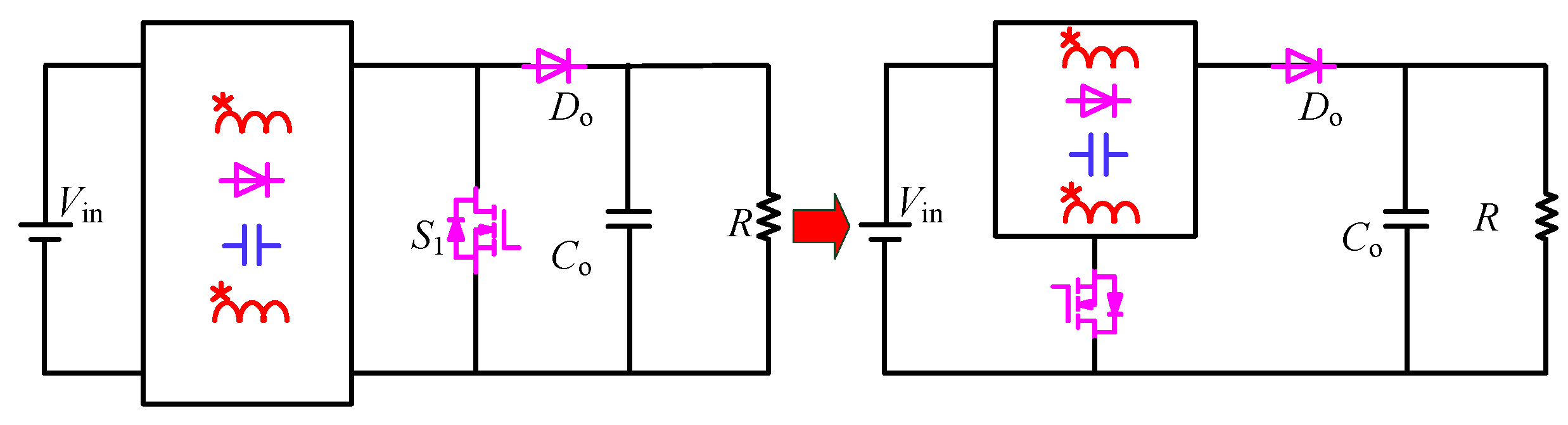
2. Proposed Topologies and Analysis
2.1. Proposed Topologies
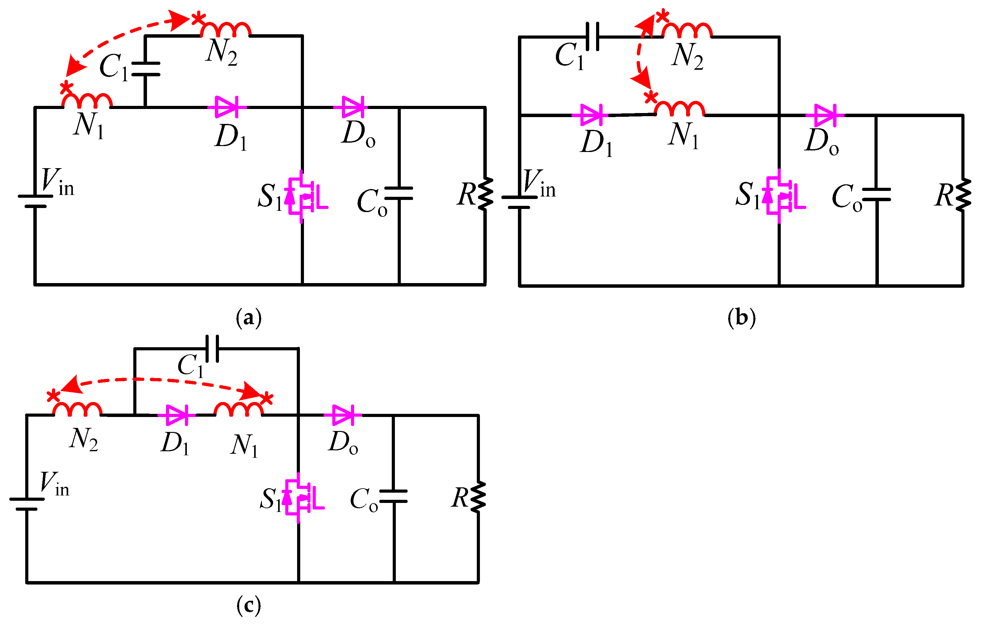
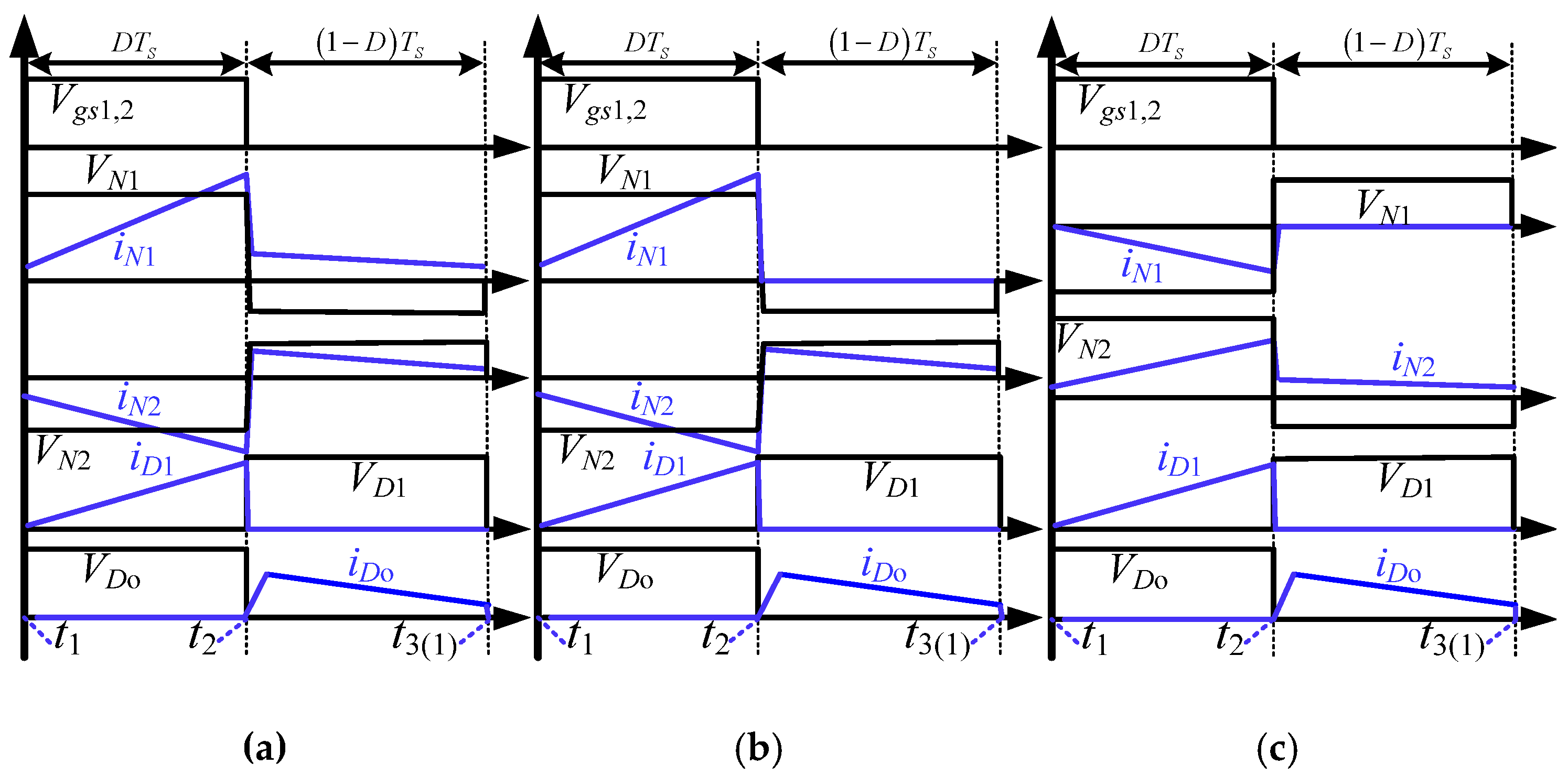
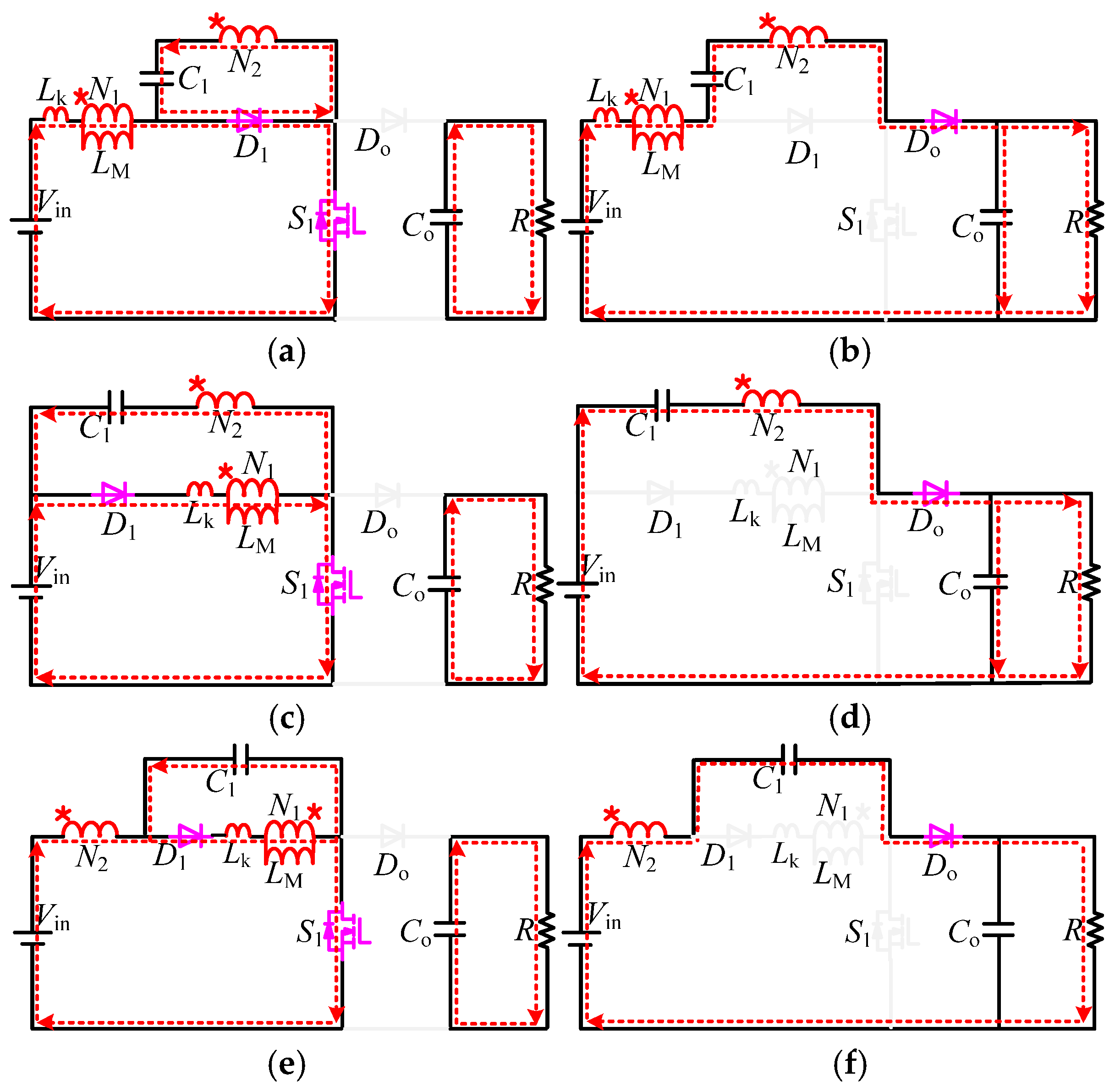
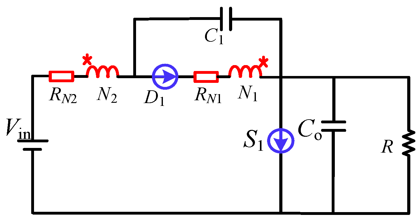
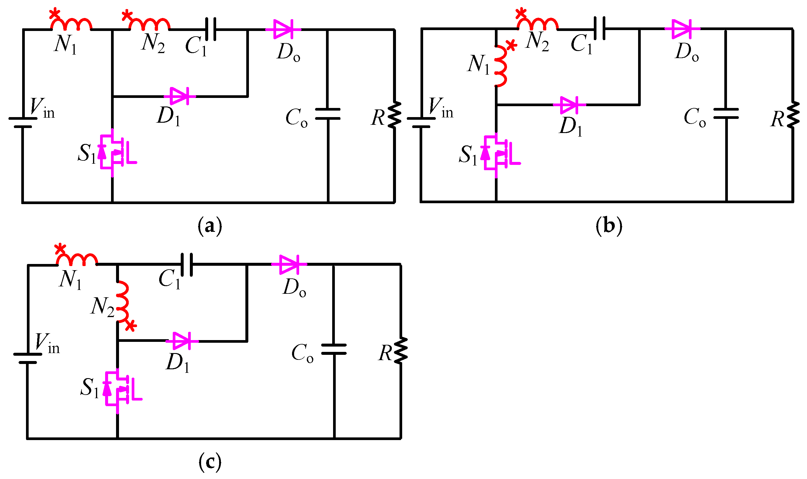
2.1.1. PWCDVD-CLBC
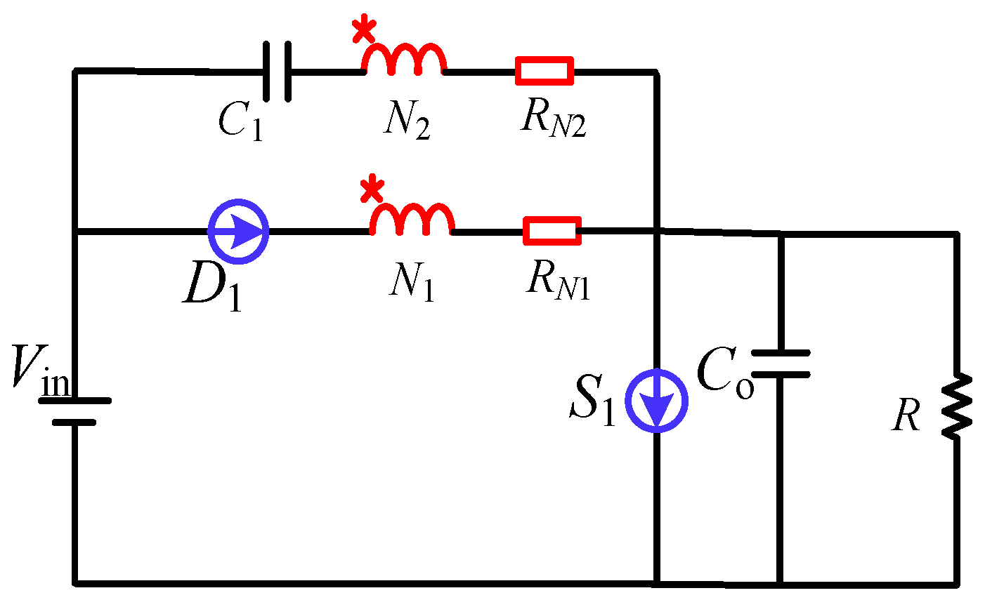
2.1.2. FPWCDVD-CLBC
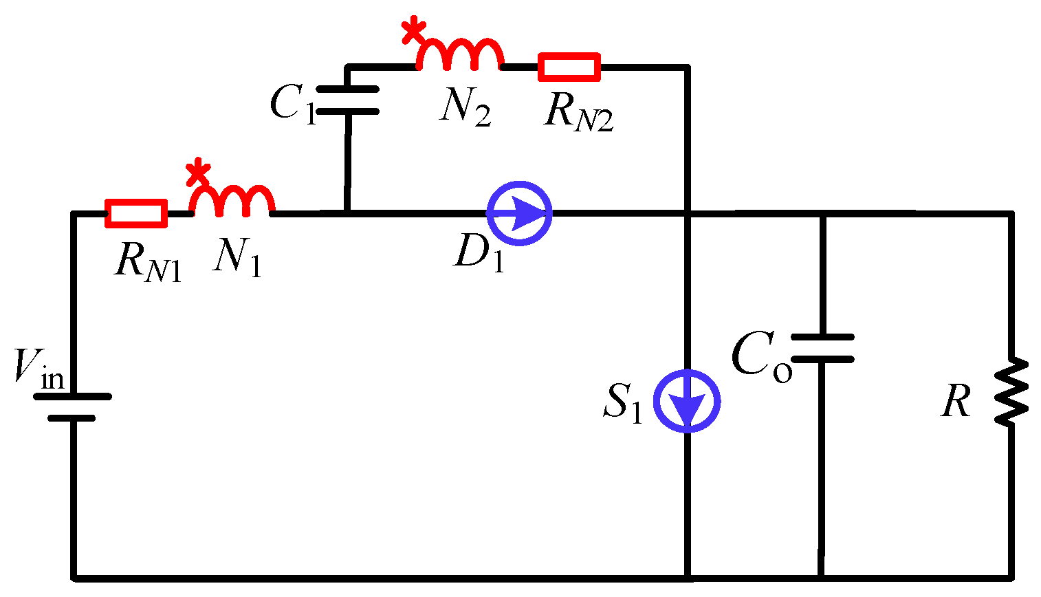
2.1.3. SWCDVD-CLBC
2.2. Math Derivation and Performance Analysis
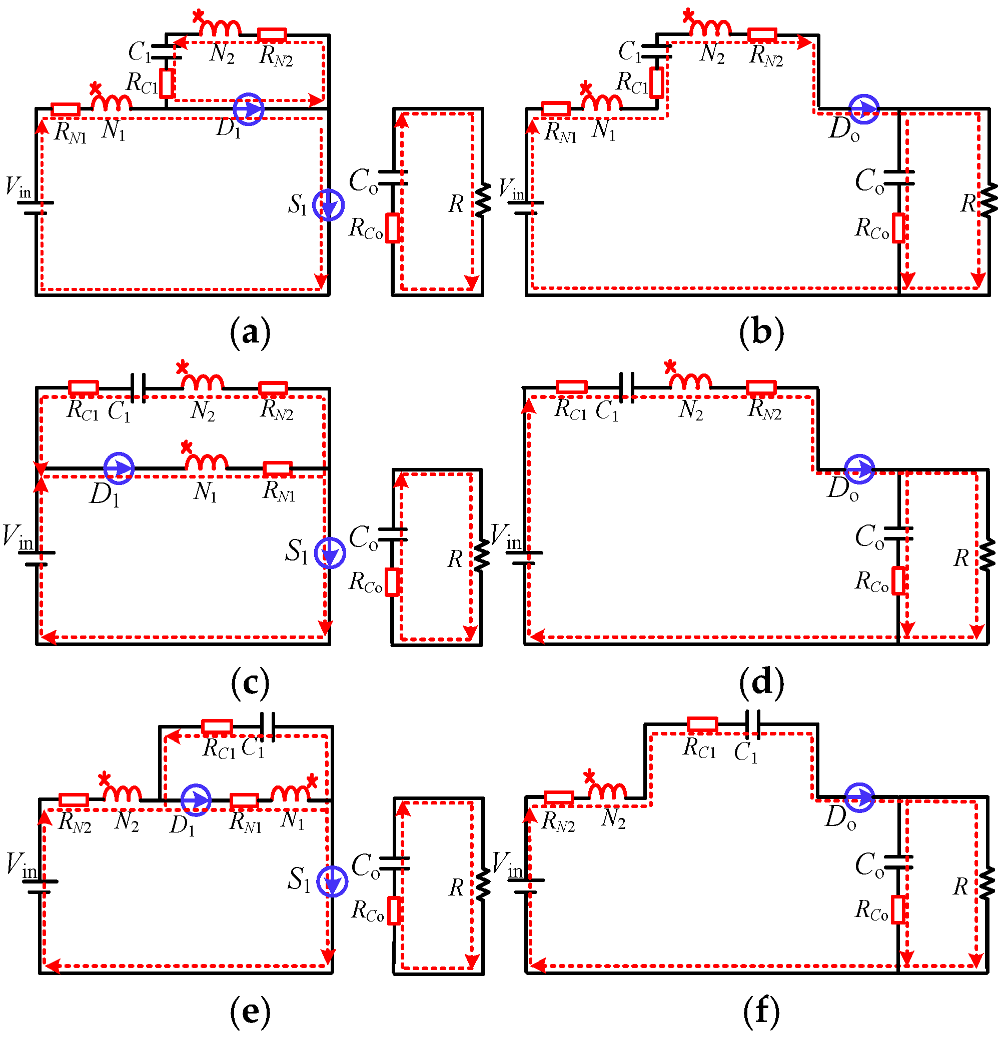
2.2.1. PWCDVD-CLBC
2.2.2. FPWCDVD-CLBC
2.2.3. SWCDVC-CLBC
2.3. Parameter Design and Performance Comparison
2.3.1. PWCDVD-CLBC
2.3.2. FPWCDVD-CLBC
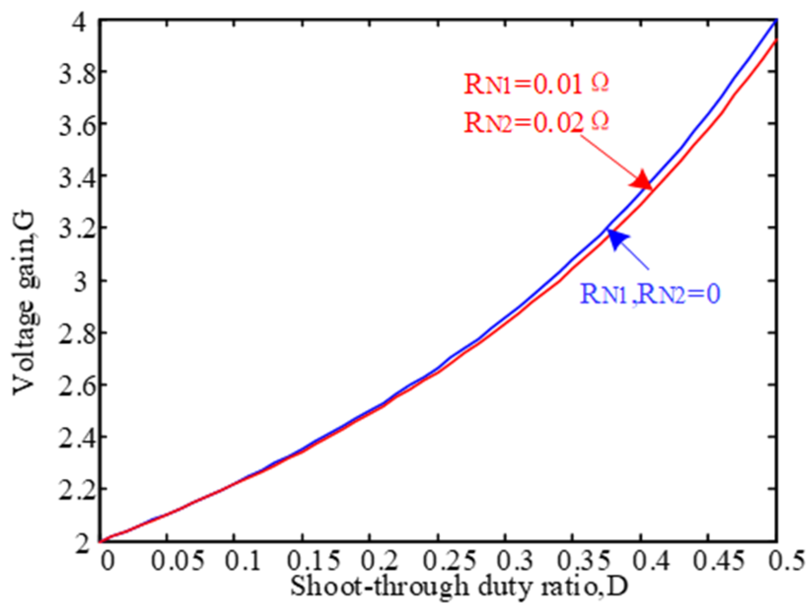
2.3.3. SWCDVD-CLBC
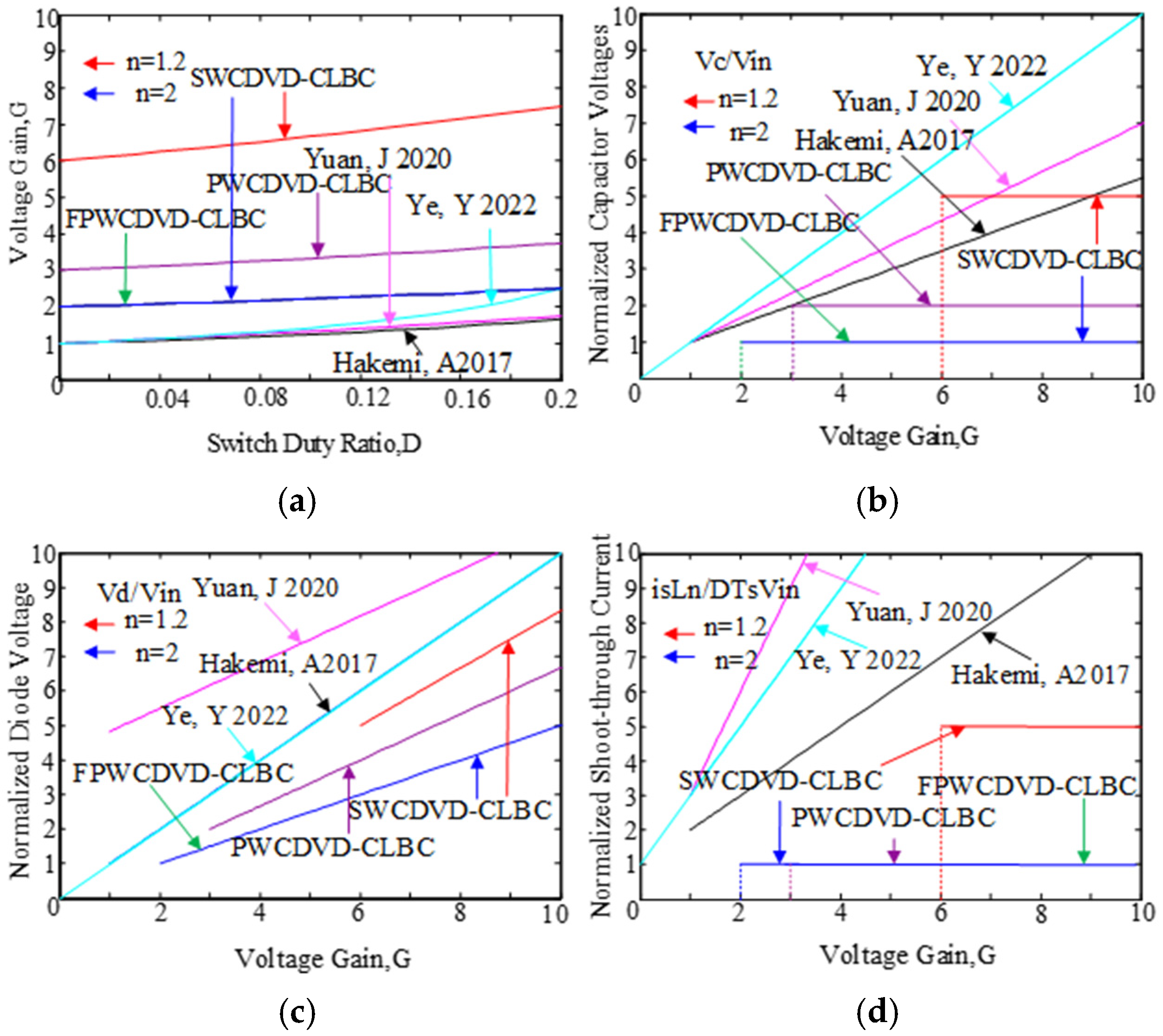
2.4. Comparative Analysis
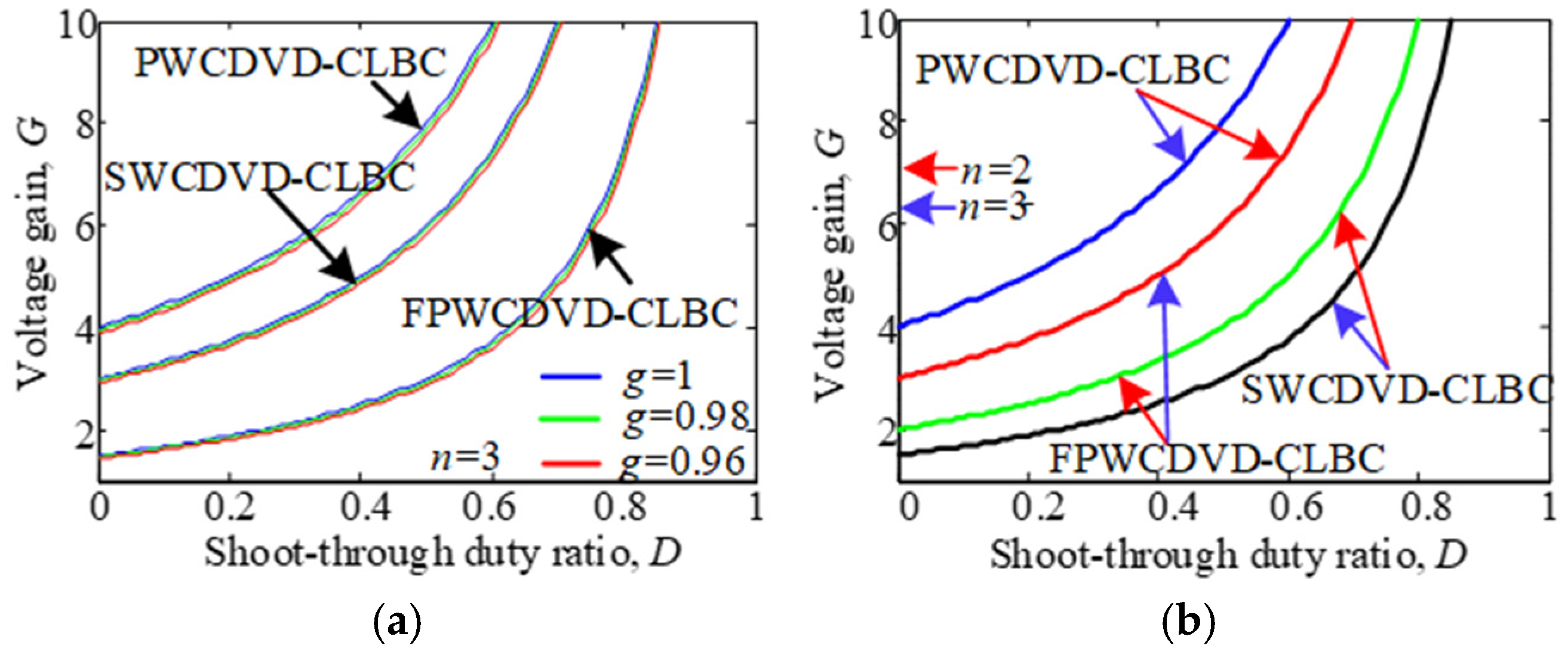
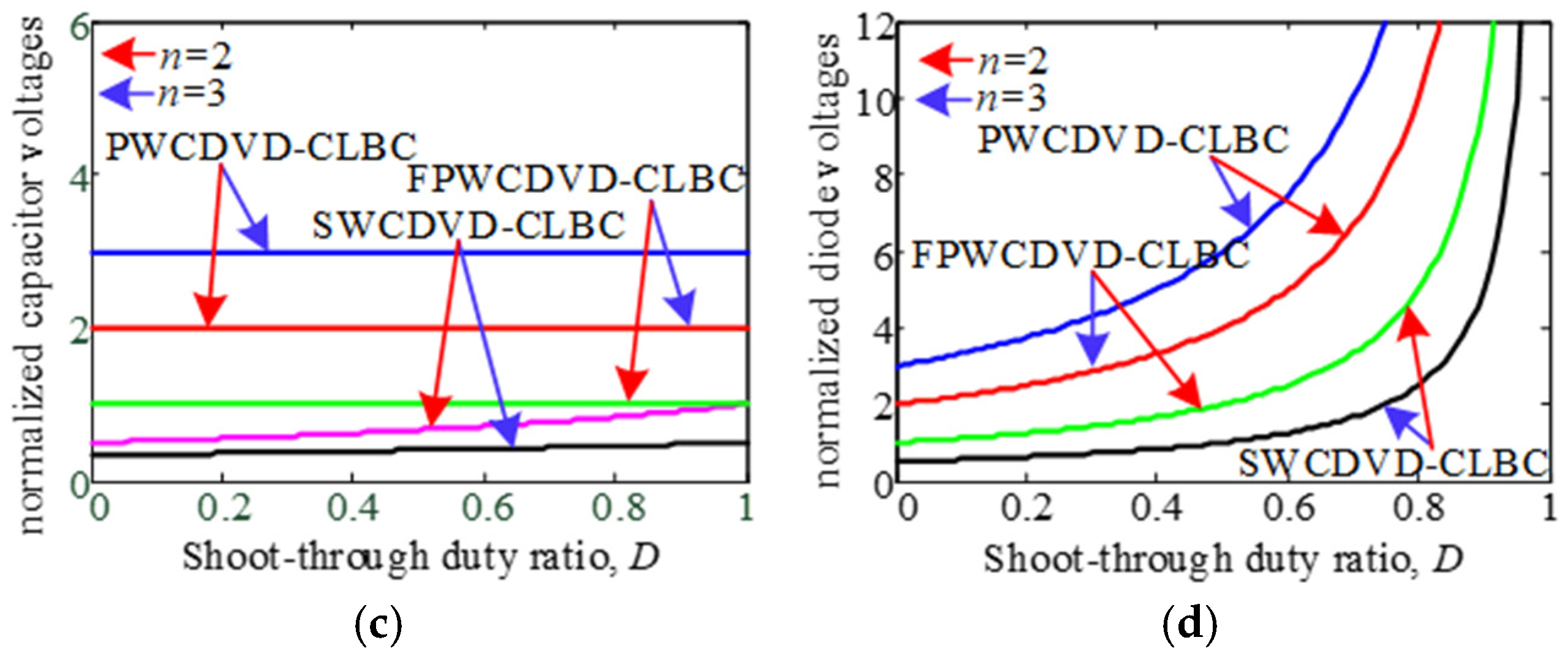
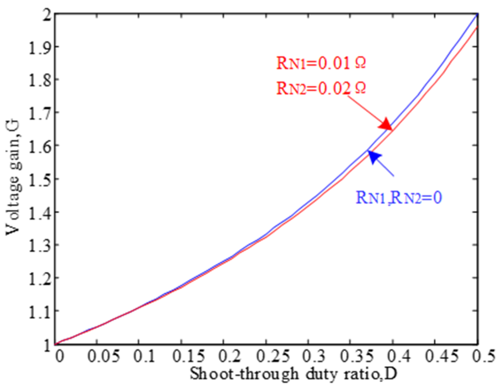
2.5. Voltage Gain Analysis
2.5.1. PWCDVD-CLBC
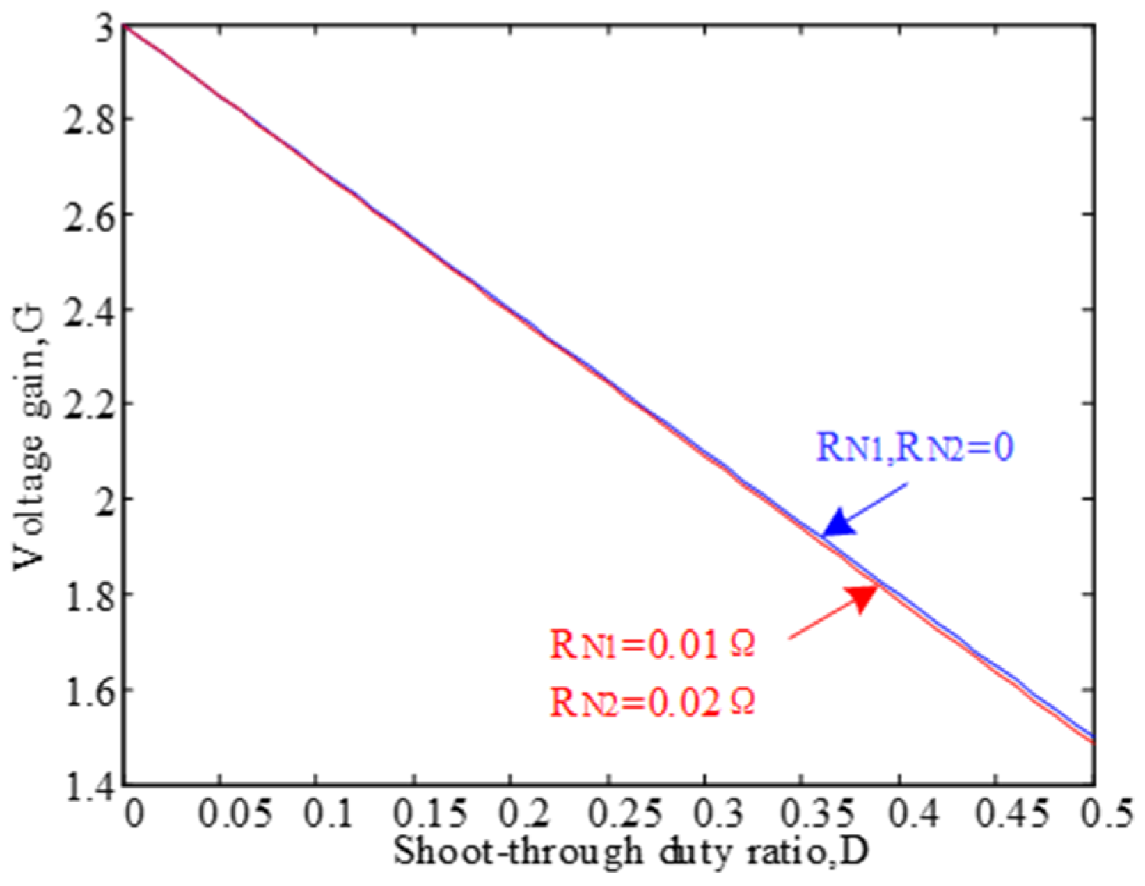
2.5.2. FPWCDVD-CLBC
2.5.3. SWCDVD-CLBC
2.6. Efficiency Calculation
2.6.1. PWCDVD-CLBC
2.6.2. FPWCDVD-CLBC
2.6.3. SWCDVD-CLBC
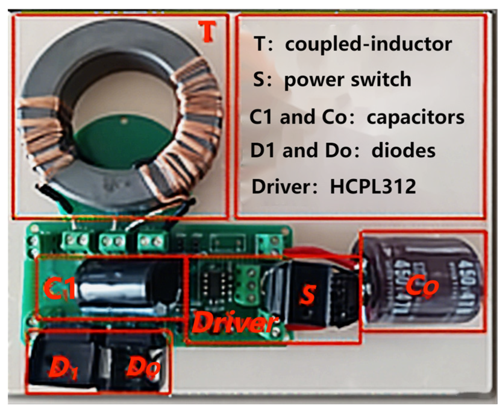
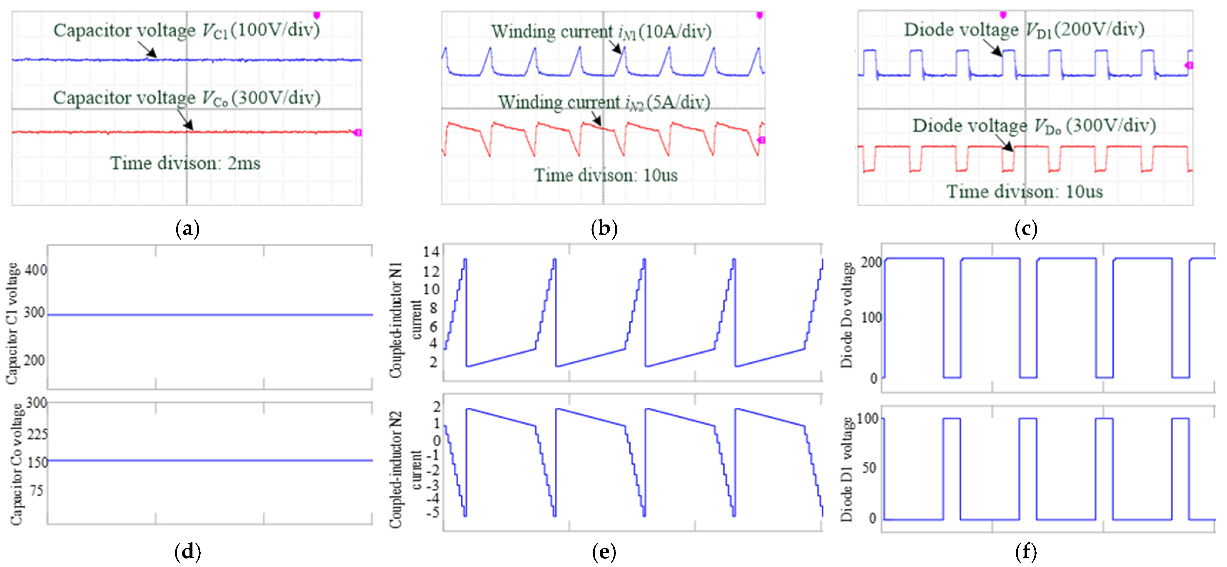
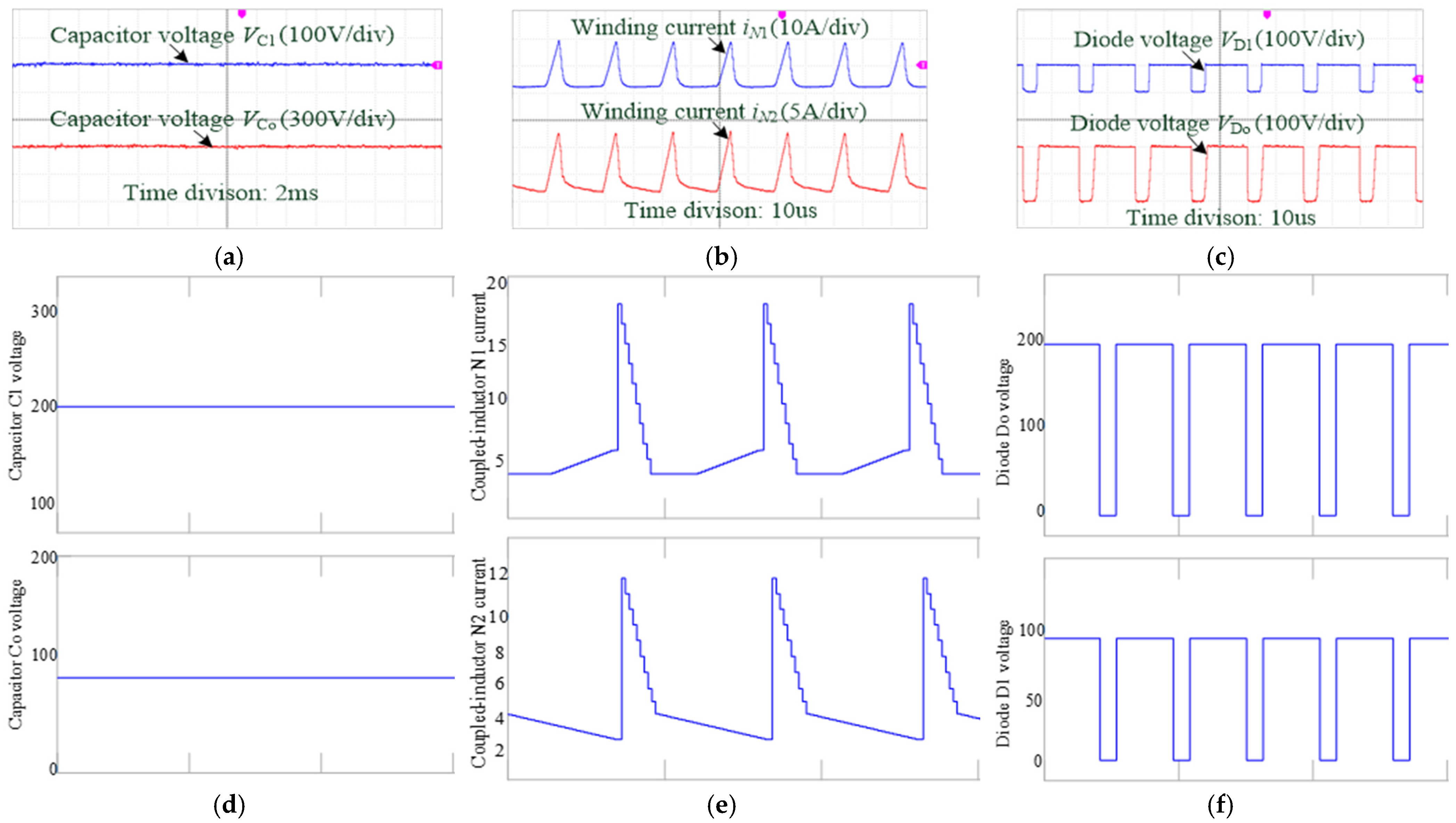
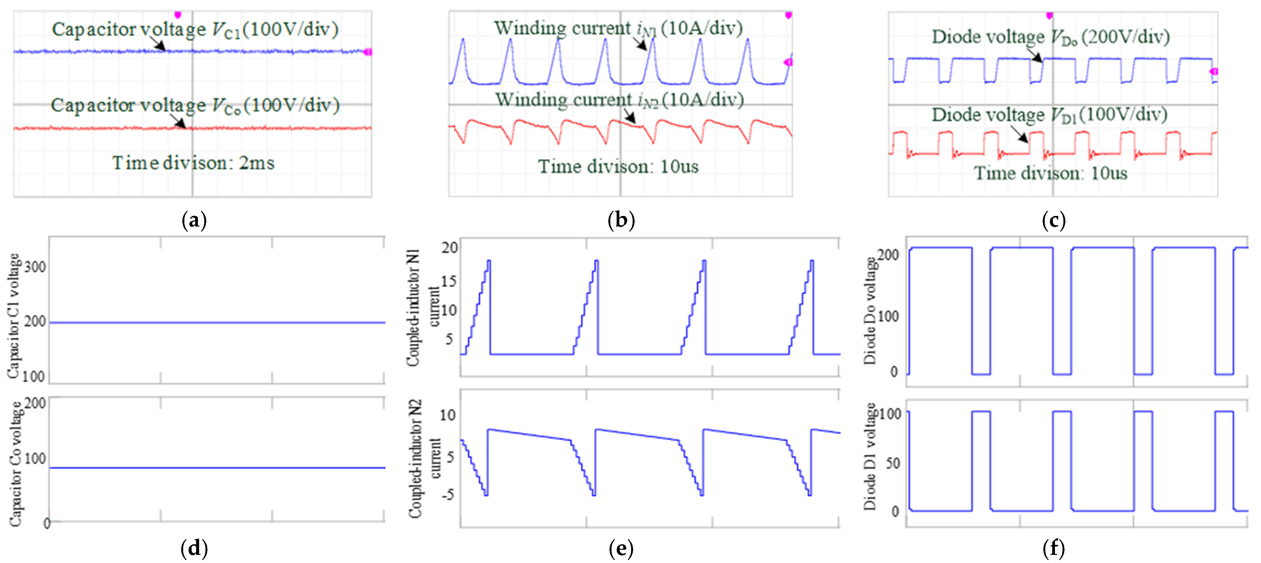
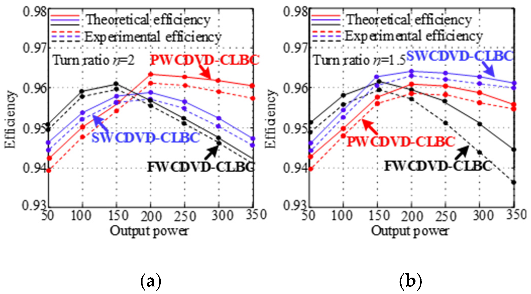
3. Results
4. Discussion
5. Conclusions
Author Contributions
Funding
Data Availability Statement
Conflicts of Interest
References
- Safayatullah, M.; Elrais, M.T.; Ghosh, S.; Rezaii, R.; Batarseh, I. A Comprehensive Review of Power Converter Topologies and Control Methods for Electric Vehicle Fast Charging Applications. IEEE Access 2022, 10, 40753–40793. [Google Scholar] [CrossRef]
- Zeng, H.; Peng, F.Z. SiC-Based Z-Source Resonant Converter with Constant Frequency and Load Regulation for EV Wireless Charger. IEEE Trans. Power Electron. 2017, 32, 8813–8822. [Google Scholar] [CrossRef]
- Zeng, H.; Wang, X.; Peng, F.Z. High power density Z source resonant wireless charger with line frequency sinusoidal charging. IEEE Trans. Power Electron. 2018, 3, 10148–10156. [Google Scholar] [CrossRef]
- Ji, Y.; Feng, Y.; Wheeler, P. High Step-Up Y-Source Coupled-Inductor Impedance Network Boost DC-DC Converters with Common Ground and Continuous Input Current. IEEE J. Emerg. Sel. Top. Power Electron. 2020, 8, 3174–3183. [Google Scholar] [CrossRef]
- Anderson, J.; Peng, F.Z. Four quasi-Z-source inverters. In Proceedings of the 2008 IEEE Power Electronics Specialists Conference, Rhodes, Greece, 5–19 June 2008; pp. 2743–2749. [Google Scholar]
- Bajestan, M.M.; Shamsinejad, M.A. Extended boost trans-Z-source inverter. In Proceedings of the 2017 8th Power Electronics, Drive Systems & Technologies Conference (PEDSTC), Mashhad, Iran, 14–16 February 2017; pp. 131–136. [Google Scholar]
- Jagan, V.; Kotturu, J.; Das, S. Enhanced-Boost Quasi-Z-Source Inverters with Two Switched Impedance Network. IEEE Trans. Ind. Electron. 2017, 64, 6885–6897. [Google Scholar] [CrossRef]
- Gu, Y.; Chen, Y.; Zhang, B. Enhanced-Boost Quasi-Z-Source Inverter with An Active Switched Z-Network. IEEE Trans. Ind. Electron. 2018, 65, 8372–8381. [Google Scholar] [CrossRef]
- Abbasi, M.; Eslahchi, A.H.; Mardaneh, M. Two Symmetric Extended-Boost Embedded Switched-Inductor Quasi-Z-Source Inverter with Reduced Ripple Continuous Input Current. IEEE Trans. Ind. Electron. 2018, 65, 5096–5104. [Google Scholar] [CrossRef]
- Fathi, H.; Madadi, H. Enhanced-Boost Z-Source Inverters with Switched Z-Impedance. IEEE Trans. Ind. Electron. 2016, 63, 691–703. [Google Scholar] [CrossRef]
- Hakemi, A.; Sanatkar-Chayjani, M.; Monfared, M. Δ-Source Impedance Network. IEEE Trans. Ind. Electron. 2017, 64, 7842–7851. [Google Scholar] [CrossRef]
- Esmaeili, S.; Sheikholeslami, A. Transformer types of extended Z-source inverter with high voltage gain and reduced transformer turns ratio. In Proceedings of the 6th Power Electronics, Drive Systems & Technologies Conference (PEDSTC2015), Tehran, Iran, 3–4 February 2015; pp. 183–188. [Google Scholar]
- Loh, P.C.; Blaabjerg, F. Magnetically coupled impedance-source inverters. IEEE Trans. Power Electron. 2013, 49, 2177–2187. [Google Scholar] [CrossRef]
- Siwakoti, Y.P.; Loh, P.C.; Blaabjerg, F.; Town, G. Y-source impedance network. In Proceedings of the 2014 IEEE Applied Power Electronics Conference and Exposition-APEC 2014, Fort Worth, TX, USA, 16–20 March 2014; pp. 3362–3366. [Google Scholar]
- Ieong, C.-F.; Leong, C.-H.; Kong, X.; Wong, C.-K.; Lam, C.-S. Effects of Parasitic Resistances on Π-Source Impedance Network. IEEE Access 2021, 9, 76403–76412. [Google Scholar] [CrossRef]
- Nguyen, M.K.; Lim, Y.C.; Park, S.J. Improved trans-Z-source inverter with continuous input current and boost inversion capability. IEEE Trans. Power Electron. 2013, 28, 4500–4510. [Google Scholar] [CrossRef]
- Eshkevari, A.L.; Mosallanejad, A.; Sepasian, M. A New Step-Up DC/DC Converter Based on LCCT Z-Source and Switched-Capacitor Cell. In Proceedings of the 2020 11th Power Electronics, Drive Systems, and Technologies Conference (PEDSTC), Tehran, Iran, 4–6 February 2020; pp. 1–6. [Google Scholar]
- Yam, P.; Blaabjerg, F.; Loh, P.C. Quasi-Y-source inverter. In Proceedings of the 2015 Australasian Universities Power Engineering Conference (AUPEC), Wollongong, Australia, 27–30 September 2015; pp. 1–5. [Google Scholar]
- Yuan, J.; Mostaan, A.; Yang, Y.; Siwakoti, Y.P.; Blaabjerg, F. A Modified Y-Source DC-DC Converter With High Voltage-Gains and Low Switch Stresses. IEEE Trans. Power Electron. 2020, 35, 7716–7720. [Google Scholar] [CrossRef]
- Siwakoti, Y.; Blaabjerg, F.; Loh, P.C. New magnetically coupled impedance (Z-) source networks. IEEE Trans. Power Electron. 2016, 31, 7419–7435. [Google Scholar] [CrossRef]
- Sharif, S.; Chulaee, Y.; Zarchi, H.A.; Monfared, M. Generalized Three-Winding Switched-Coupled-Inductor Impedance Networks With Highly Flexible Gain. IEEE Trans. Ind. Electron. 2021, 68, 2130–2141. [Google Scholar] [CrossRef]
- Nguyen, M.K.; Le, T.V.; Park, S.J.; Lim, Y.C. A class of quasi switched boost inverters. IEEE Trans. Ind. Electron. 2015, 62, 1526–1536. [Google Scholar] [CrossRef]
- Nguyen, M.; Young-Cheol, L.; Joon-Ho, C.; Youn-Ok, C. Trans-switched boost inverters. IET Power Electron. 2016, 9, 1065–1073. [Google Scholar] [CrossRef]
- Ye, Y.; Xu, S.; Chen, S.; Wang, X.; Cao, L. High-Gain Quasi-Switched Boost Inverter with Single Inductor and Continuous Input Current. IEEE Trans. Power Electron. 2022, 37, 10106–10111. [Google Scholar] [CrossRef]
- Sharifi, S.; Monfared, M. Series and Tapped Switched-Coupled-Inductors Impedance Networks. IEEE Trans. Ind. Electron. 2018, 65, 9498–9508. [Google Scholar] [CrossRef]
- Pan, L. L-Z-source inverter. IEEE Trans. Power Electron. 2014, 29, 6534–6543. [Google Scholar] [CrossRef]

| Topology | G | Component Count | Input Current |
|---|---|---|---|
| Z-source converter | 4 | Discontinuous | |
| Quasi-switched boost converter | 11 | Continuous | |
| Modified-Y-source network | 12 | Continuous | |
| Δ-Source network | 9 | Discontinuous | |
| Y-source impedance network | 8 | Discontinuous | |
| Extended Z-source | 10 | Discontinuous | |
| Π-source impedance network | 7 | Discontinuous | |
| extended boost trans-Z-source inverter | 9 | Continuous | |
| Switched-inductor-Z-source | 13 | Continuous | |
| L-Z-source inverter | 5 | Continuous | |
| Trans-switched boost inverters | 6 | Discontinuous | |
| Quasi-Y-source inverter | 7 | Continuous | |
| LCCT Z-source | 8 | Continuous | |
| Improved trans-Z-source inverter | 6 | Continuous | |
| Three-winding switched-coupled inductor (PSCL) | 9 | Continuous |
| Symbol | Description | Unit |
|---|---|---|
| Vin | Input voltage | V |
| Co | Output capacitor voltage | V |
| D1 | Diode | - |
| LK | Leakage inductance | H |
| LM | Magnetizing inductance | H |
| C1 | Intermediate capacitor | F |
| R | Load resistance | Ω |
| N1/2 | Primary/secondary edge | - |
| S1 | Switch | - |
| Parameters | Δ-Source Network [11] | Modified-Y-Source Network [19] | Quasi-Switched Network [24] | PWCDVD-CLBC | FPWCDVD-CLBC | SWCDVD-CLBC |
|---|---|---|---|---|---|---|
| G | ||||||
| VC-max | ||||||
| VD-max | ||||||
| Shoot-through peak current | ||||||
| Component count | 9 | 12 | 11 | 5 | 5 | 5 |
| Input current | Discontinuous | Continuous | Continuous | Continuous | Continuous | Continuous |
| Cost | Medium | High | Medium | Low | Low | Low |
| Parameter | Description | Experiment/Value |
|---|---|---|
| Input Voltage | Vin | 80 V |
| Output Voltage | Vo | 300 V, 200 V, 200 V |
| Switch frequency | f | 50 kHZ |
| Duty ratio | D | 0.2 |
| Output power | P | 300 W |
| Capacitor | C1 | 240 uF |
| Capacitor | Co | 440 uF |
| Magnetic core material | / | PC40 |
| Maximum magnetic flux density | Bs | 0.4 T |
| Hysteresis loss coefficient | Ch | 1 × 10⁻⁷/mT |
| Effective permeability | μe | 2400 ± 20% |
| Turn ratio | n | 16:8 |
| Diode | D1 | SF1005G (10 A/300 V) |
| Diode | Do | MUR1070 (1.5 A/700 V) |
| Switch | S1 | IPW65R019C7 |
| MOSFET driver | / | HCPL3120 |
Disclaimer/Publisher’s Note: The statements, opinions and data contained in all publications are solely those of the individual author(s) and contributor(s) and not of MDPI and/or the editor(s). MDPI and/or the editor(s) disclaim responsibility for any injury to people or property resulting from any ideas, methods, instructions or products referred to in the content. |
© 2025 by the authors. Licensee MDPI, Basel, Switzerland. This article is an open access article distributed under the terms and conditions of the Creative Commons Attribution (CC BY) license (https://creativecommons.org/licenses/by/4.0/).
Share and Cite
Ji, Y.; Ji, S.; Liu, Y. High-Gain Coupled-Inductor Boost Converters Using Voltage-Doubling and Continuous Input Current Design. Electronics 2025, 14, 2659. https://doi.org/10.3390/electronics14132659
Ji Y, Ji S, Liu Y. High-Gain Coupled-Inductor Boost Converters Using Voltage-Doubling and Continuous Input Current Design. Electronics. 2025; 14(13):2659. https://doi.org/10.3390/electronics14132659
Chicago/Turabian StyleJi, Yuliang, Shuai Ji, and Yiqi Liu. 2025. "High-Gain Coupled-Inductor Boost Converters Using Voltage-Doubling and Continuous Input Current Design" Electronics 14, no. 13: 2659. https://doi.org/10.3390/electronics14132659
APA StyleJi, Y., Ji, S., & Liu, Y. (2025). High-Gain Coupled-Inductor Boost Converters Using Voltage-Doubling and Continuous Input Current Design. Electronics, 14(13), 2659. https://doi.org/10.3390/electronics14132659