
Challenges in the Design and Development of Slow-Wave Structure for THz Traveling-Wave Tube: A Tutorial Review


Abstract
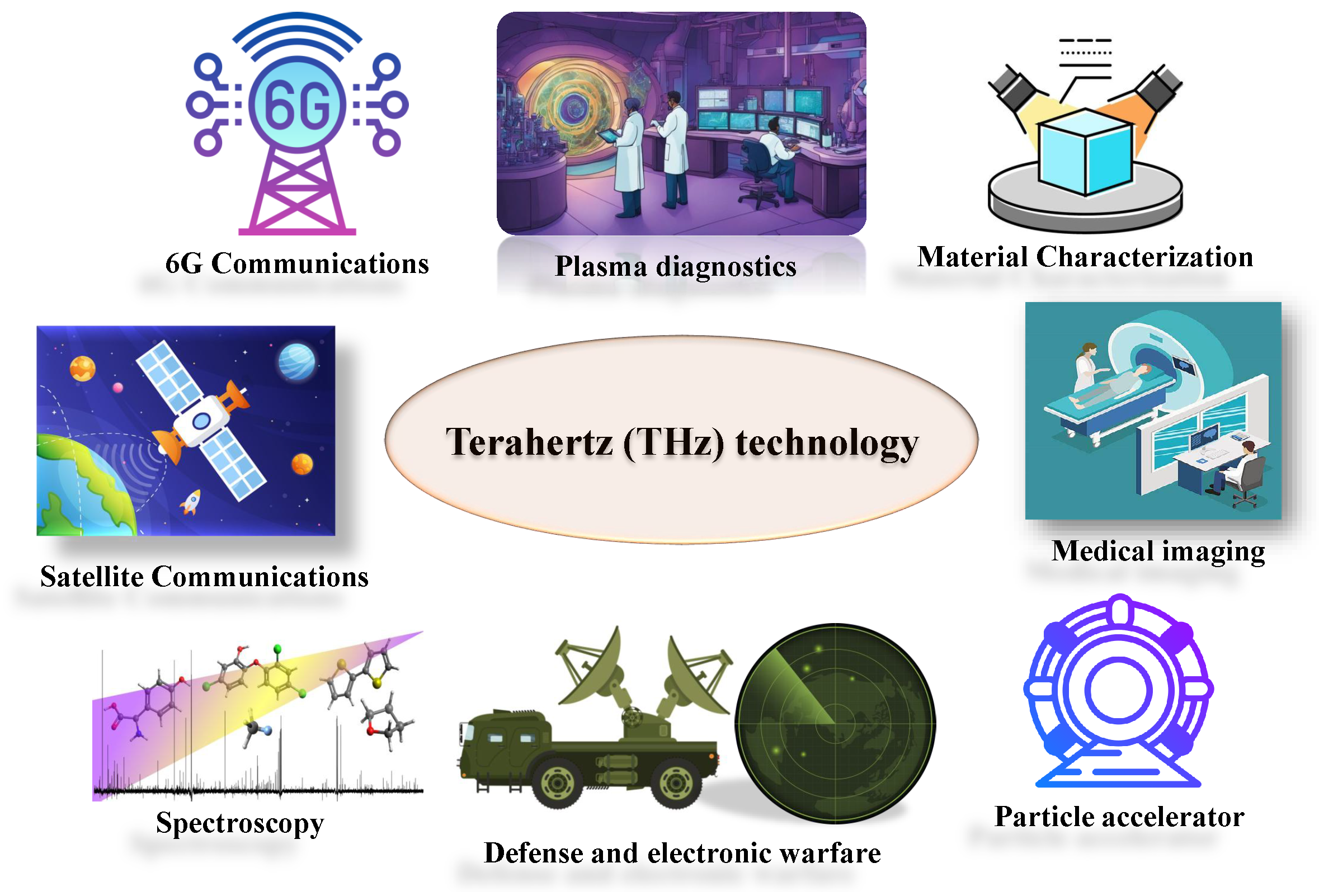
1. Introduction
- To outline a step-by-step design methodology for SWSs in traveling-wave tubes (TWTs) operating in the THz frequency band.
- To identify the challenges in designing SWSs and propose potential solutions to overcome them.
- To present a case study by designing a staggered double vane (SDV) structure operating at 1 THz frequency.
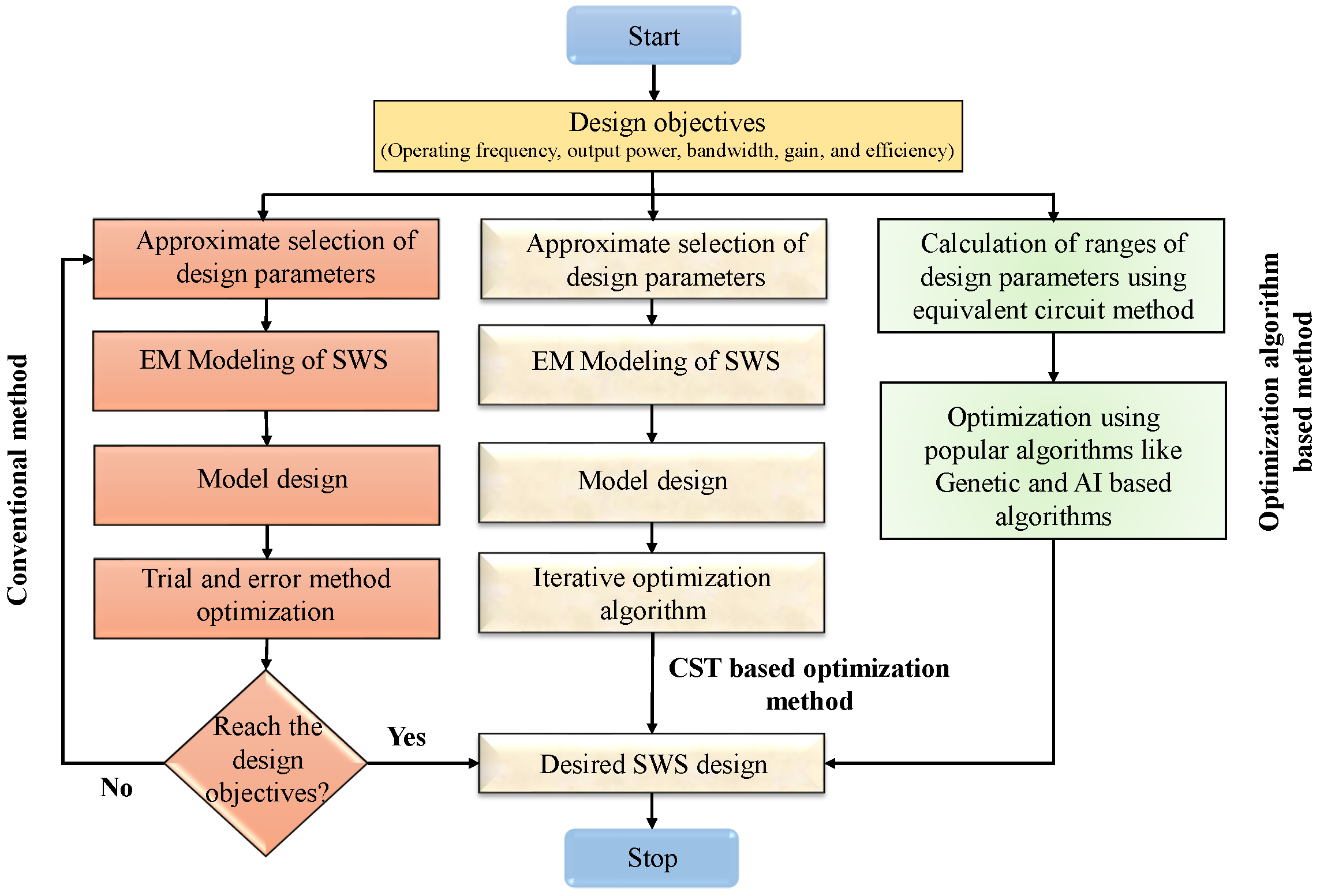
2. Design Methodology of SWS at THz Frequency
2.1. Initialization
2.2. Characteristics Analysis
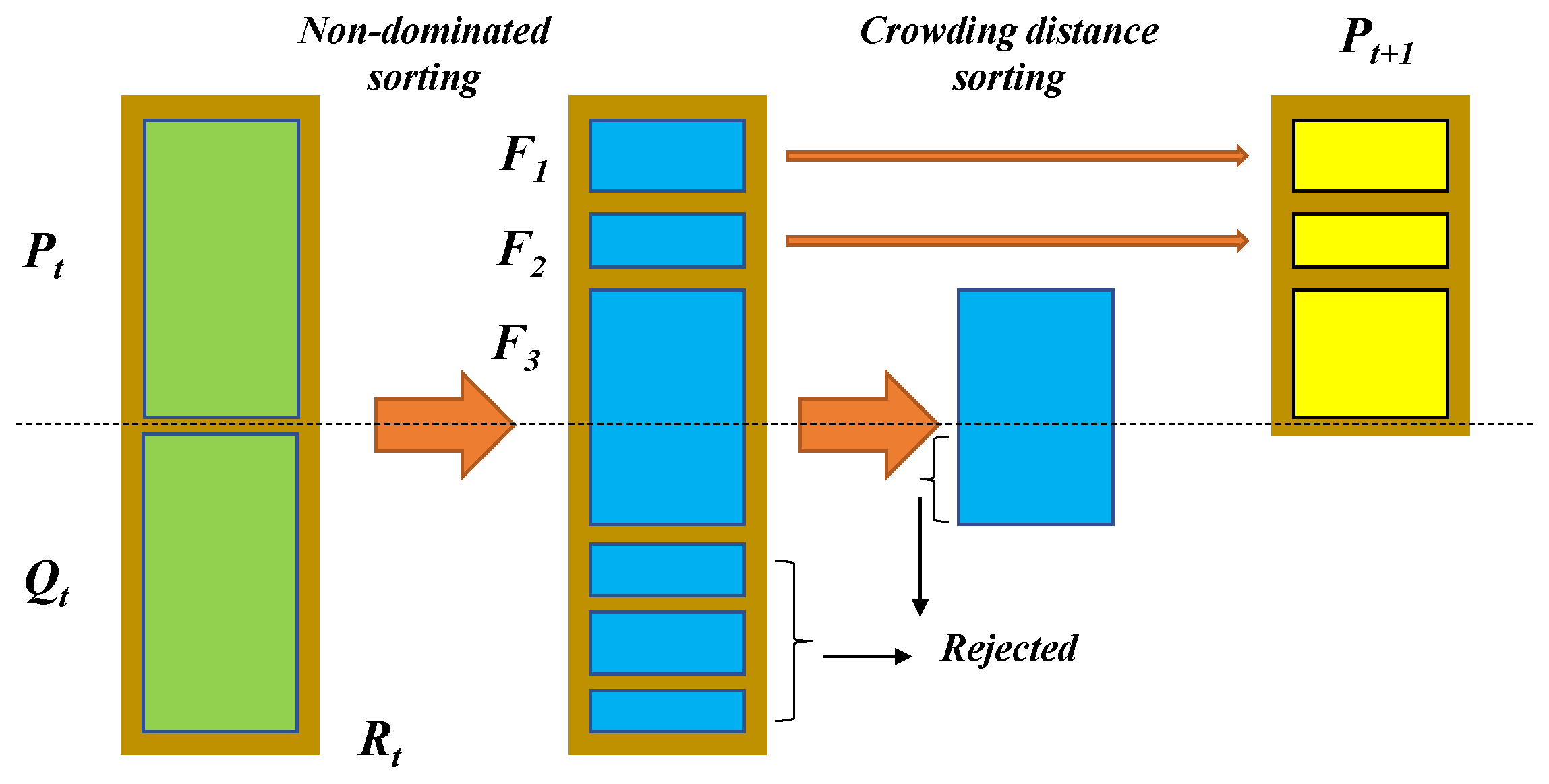
2.3. Prototype and Validation
3. Challenges and Possible Solutions in the Design of SWS for THz-TWT
3.1. Finding the Design Parameters of SWS
3.2. Selection of the Input Parameters
3.3. Phase Velocity Mismatch
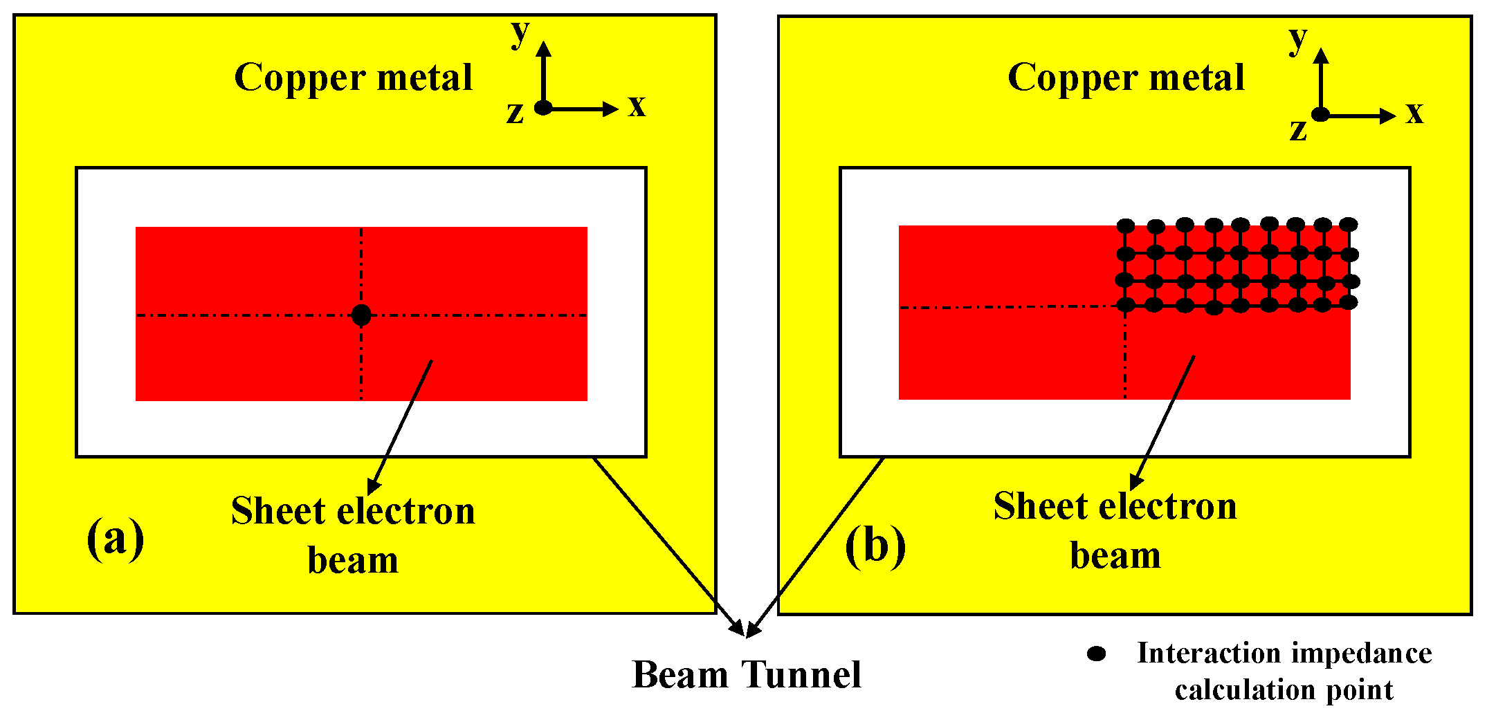
3.4. Interaction or Coupling Impedance
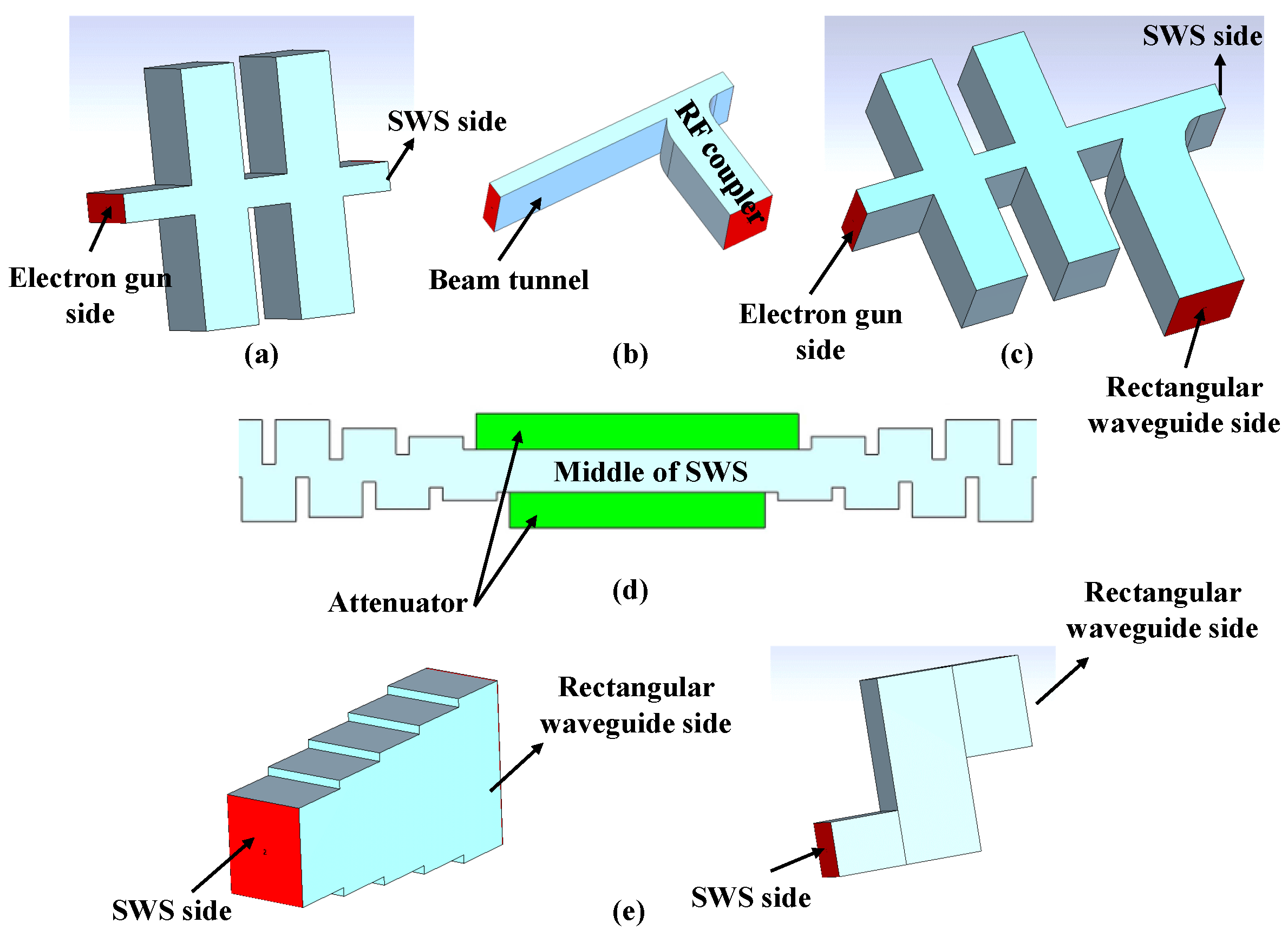
3.5. Design of Reflector, RF Coupler, Attenuator, and Transition Section
3.6. Filling Factor
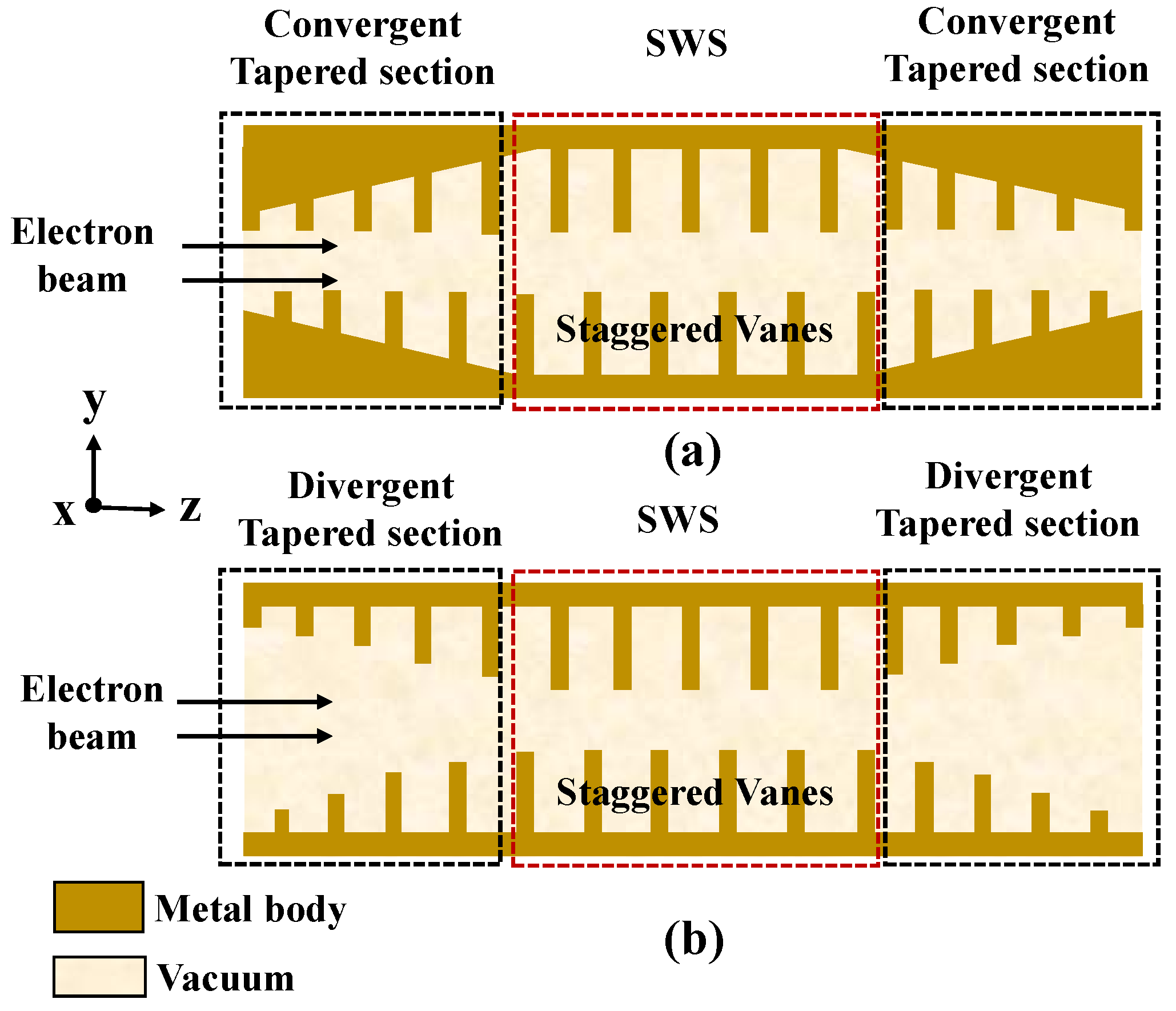
3.7. Tapered Section
3.8. Material Selection

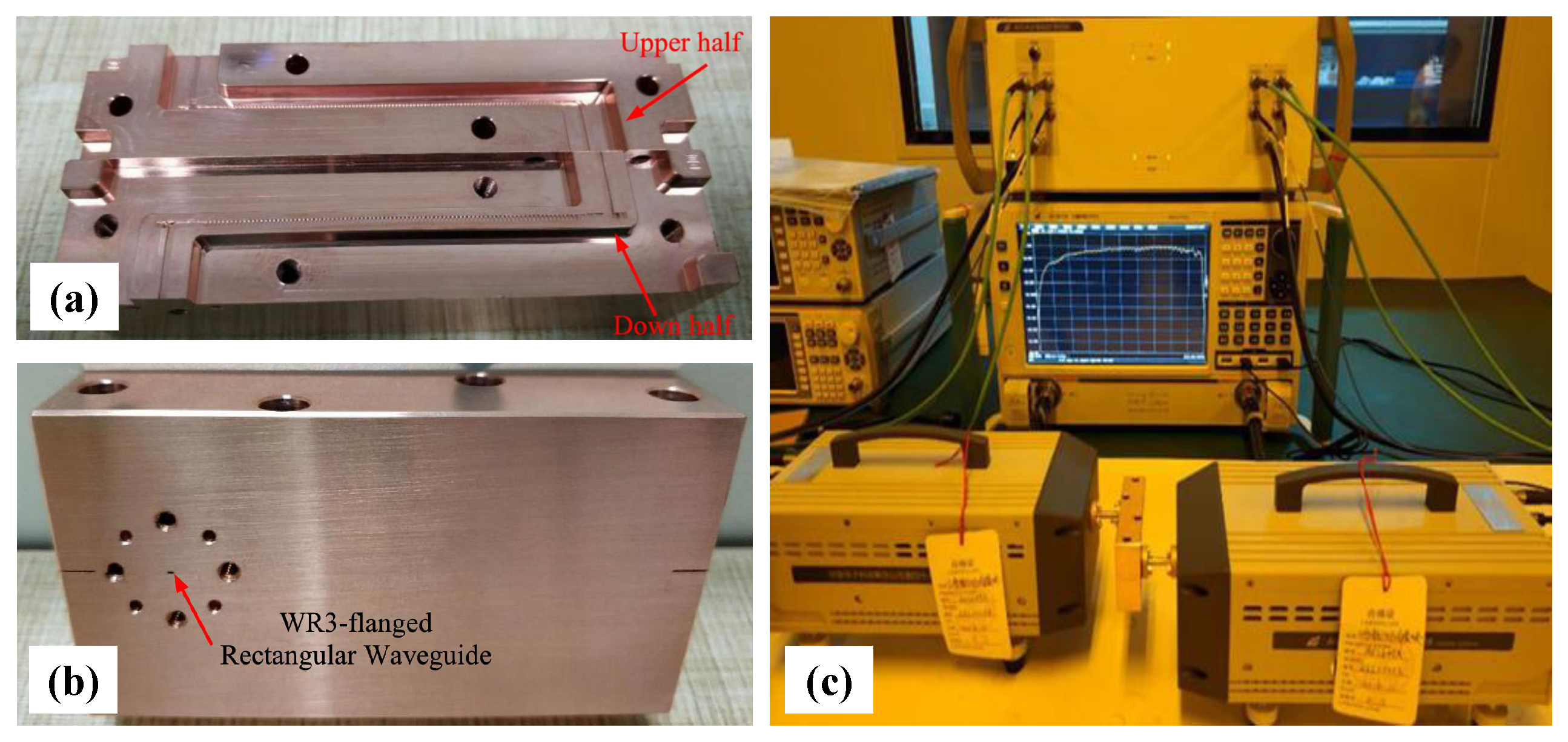
3.9. Fabrication Difficulties at THz
3.10. Fabrication Tolerance Analysis
3.11. Application of Slow-Wave Structures in Other Components
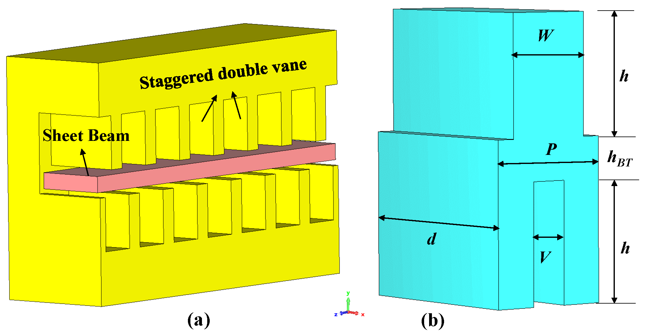
4. Case Study: Design of THz Staggered Double Vane Slow-Wave Structure
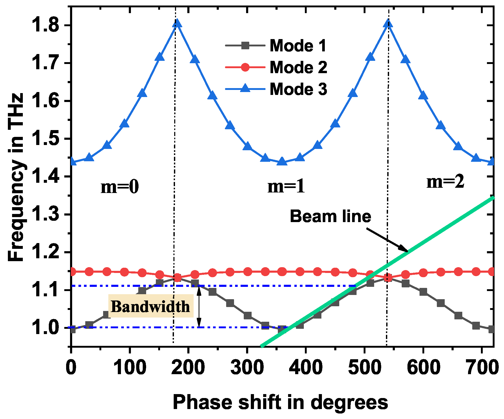
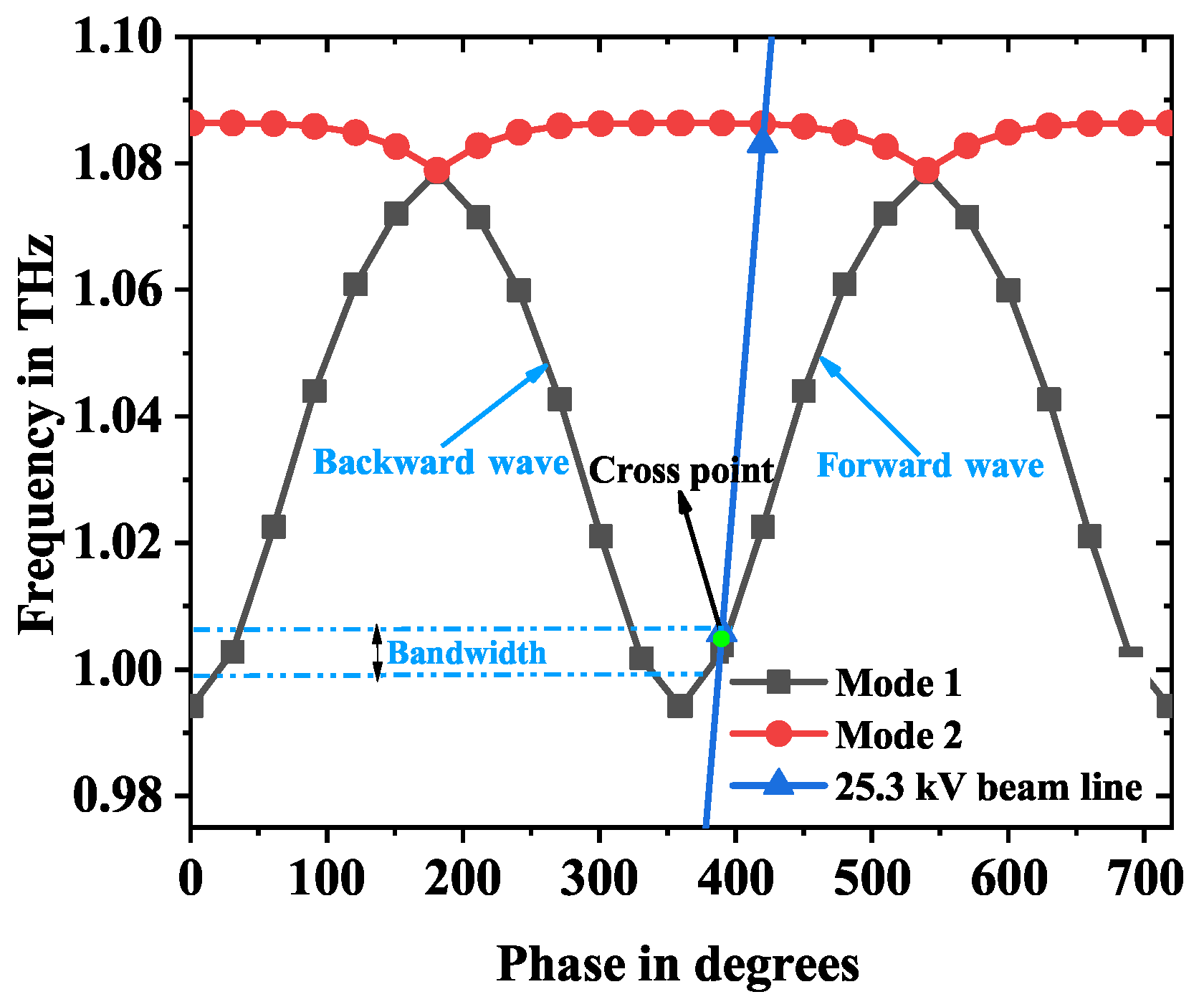
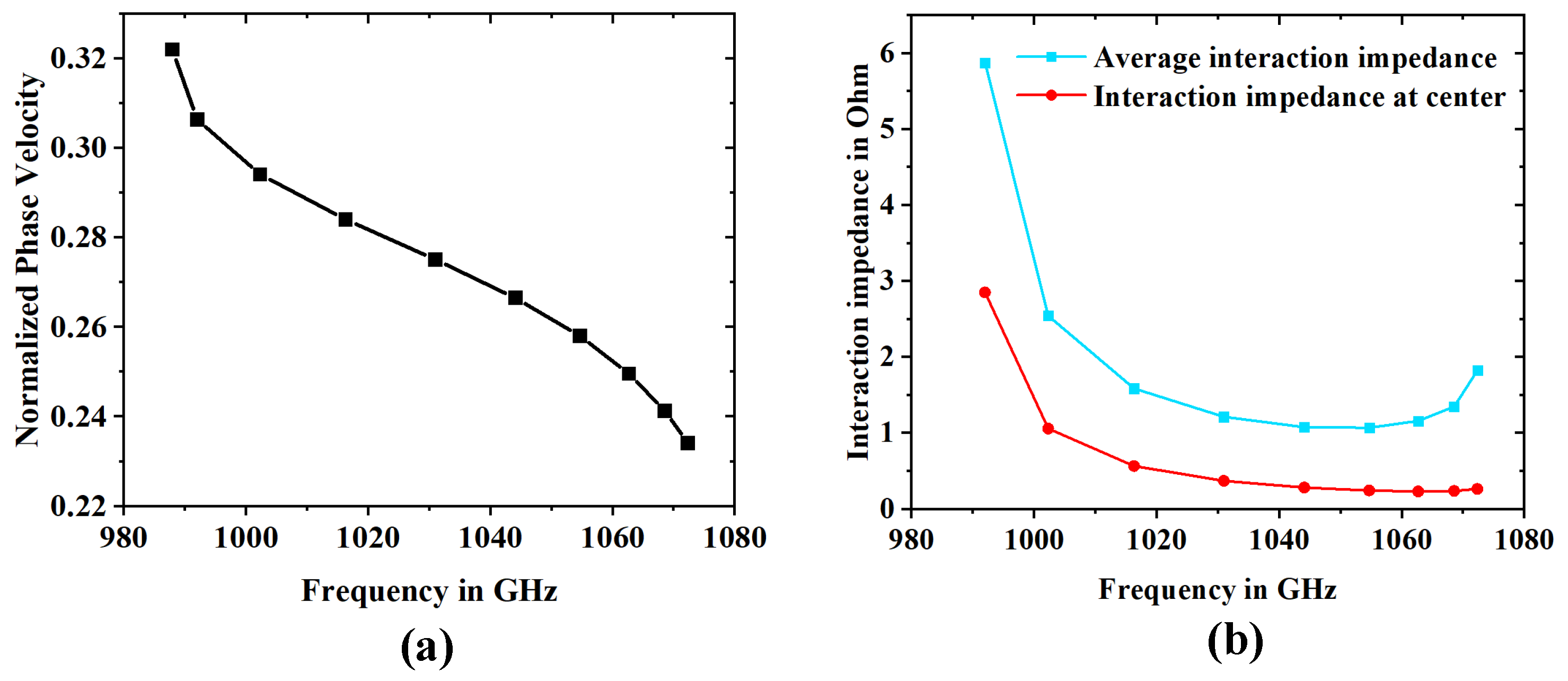
4.1. Single Cell Design and Dispersion Characteristics
4.2. Transmission Characteristics of SDV-SWS
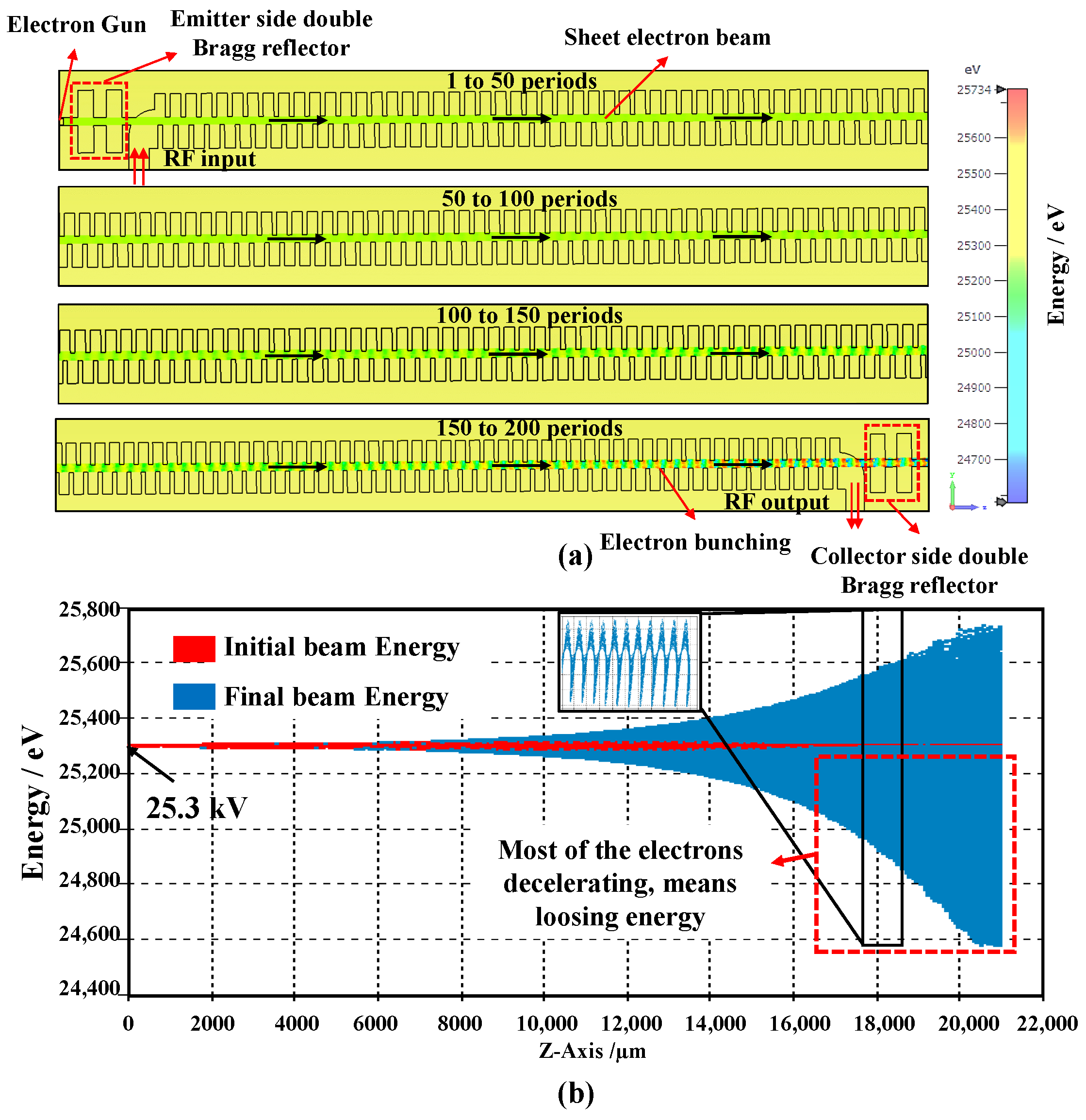
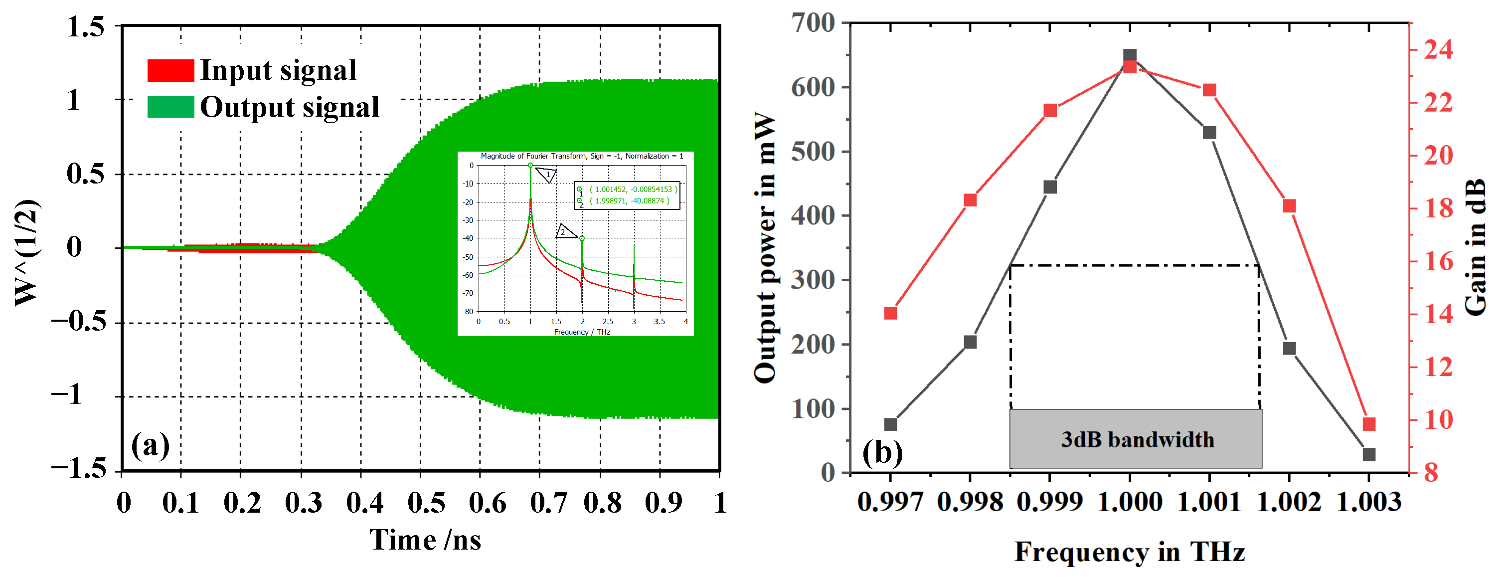
4.3. Beam–Wave Interaction Analysis
5. Conclusions
Author Contributions
Funding
Data Availability Statement
Conflicts of Interest
References
- Gilmour, A. Klystrons, Traveling Wave Tubes, Magnetrons, Crossed Field Amplifiers, and Gyrotrons; Artech House: Norwood, MA, USA, 2011. [Google Scholar]
- Collins, G.B. Microwave Magnetron, 6th ed.; McGraw-Hill: New York, NY, USA, 1948. [Google Scholar]
- Benford, J.; Schamiloglu, E.; Stephens, J.C.; Swegle, J.A.; Zhang, P. High Power Microwaves, 4th ed.; CRC Press: Boca Raton, FL, USA, 2024. [Google Scholar] [CrossRef]
- Benford, J. History and Future of High Power Microwaves. IEEE Trans. Plasma Sci. 2024, 52, 1137–1144. [Google Scholar] [CrossRef]
- Cai, J.; Feng, J.; Wu, X. Folded Waveguide Slow Wave Structure with Modified Circular Bends. IEEE Trans. Electron. Devices 2014, 61, 3534–3538. [Google Scholar] [CrossRef]
- Sumathy, M.; Vinoy, K.J.; Datta, S.K. Analysis of Ridge-Loaded Folded-Waveguide Slow-Wave Structures for Broadband Traveling-Wave Tubes. IEEE Trans. Electron. Devices 2010, 57, 1440–1446. [Google Scholar] [CrossRef]
- Zhang, Z.; Ruan, C.; Wang, W.; Fahad, A.K.; Pan, P.; He, W. G-Band High-Power and Ultrawide Band Staggered Double-Vane Slow-Wave Circuit with Double Beams. IEEE Trans. Terahertz Sci. Technol. 2022, 12, 23–29. [Google Scholar] [CrossRef]
- Wang, W.; Zhang, Z.; Wang, P.; Zhao, Y.; Zhang, F.; Ruan, C. Double-mode and double-beam staggered double-vane traveling-wave tube with high-power and broadband at terahertz band. Sci. Rep. 2022, 12, 12012. [Google Scholar] [CrossRef]
- Zhang, Z.; Ruan, C.; Fahad, A.K.; Zhang, C.; Su, Y.; Wang, P.; He, W. Multiple-beam and double-mode staggered double vane travelling wave tube with ultra-wide band. Sci. Rep. 2020, 10, 20159. [Google Scholar] [CrossRef]
- Wan, Y.; Wang, J.; Liu, Q.; Li, X.; Wu, Z.; Liu, G.; Luo, Y. A High-Power Sheet Beam Slow-Wave Structure of Traveling Wave Tubes. IEEE Electron. Device Lett. 2021, 42, 747–750. [Google Scholar] [CrossRef]
- Tian, Y.; Yue, L.; Wang, H.; Zhou, Q.; Wei, Y.; Hao, B.; Wei, Y.; Gong, Y. Investigation of Ridge-Loaded Folded Rectangular Groove Waveguide Slow-Wave Structure for High-Power Terahertz TWT. IEEE Trans. Electron. Devices 2018, 65, 2170–2176. [Google Scholar] [CrossRef]
- Lu, Z.; Zhu, M.; Ding, K.; Wen, R.; Ge, W.; Wang, Z.; Tang, T.; Gong, H.; Gong, Y. Investigation of Double Tunnel Sine Waveguide Slow-Wave Structure for Terahertz Dual-Beam TWT. IEEE Trans. Electron. Devices 2020, 67, 2176–2181. [Google Scholar] [CrossRef]
- Fang, S.; Xu, J.; Yin, H.; Lei, X.; Jiang, X.; Yin, P.; Wu, G.; Yang, R.; Li, Q.; Guo, G.; et al. Experimental Verification of the Low Transmission Loss of a Flat-Roofed Sine Waveguide Slow-Wave Structure. IEEE Electron. Device Lett. 2019, 40, 808–811. [Google Scholar] [CrossRef]
- Zhang, L.; Jiang, Y.; Lei, W.; Hu, P.; Guo, J.; Song, R.; Tang, X.; Ma, G.; Chen, H.; Wei, Y. A piecewise sine waveguide for terahertz traveling wave tube. Sci. Rep. 2022, 12, 10449. [Google Scholar] [CrossRef] [PubMed]
- Yang, R.; Xu, J.; Yin, P.; Wu, G.; Fang, S.; Jiang, X.; Luo, J.; Yue, L.; Yin, H.; Zhao, G.; et al. Study on 1-THz Sine Waveguide Traveling-Wave Tube. IEEE Trans. Electron. Devices 2021, 68, 2509–2514. [Google Scholar] [CrossRef]
- Yang, R.; Xu, J.; Yue, L.; Yin, P.; Luo, J.; Yin, H.; Zhao, G.; Guo, G.; Yu, S.; Niu, X.; et al. Design and Experiment of 1 THz Slow Wave Structure Fabricated by Nano-CNC Technology. IEEE Trans. Electron. Devices 2022, 69, 2656–2661. [Google Scholar] [CrossRef]
- Wang, Z.; Zhu, J.; Lu, Z.; Duan, J.; Chen, H.; Wang, S.; Wang, Z.; Gong, H.; Gong, Y. A Novel Staggered Double-Segmented Grating Slow-Wave Structure for 340 GHz Traveling-Wave Tube. Sensors 2023, 23, 4762. [Google Scholar] [CrossRef]
- Lee, J.; Choi, H.E.; Choi, W.; Choi, E. Advanced Bragg Resonator Integration for Enhanced Bandwidth and Stability in G-Band TWT with Staggered Double Vane Structure. IEEE Trans. Electron. Devices 2025, 72, 459–466. [Google Scholar] [CrossRef]
- Stanislaus, R.J.; Bera, A.; Sharma, R.K. Design and Analysis of a Wideband Staggered Double-Vane Slow-Wave Structure for W-Band Amplifier. IEEE Trans. Plasma Sci. 2021, 49, 251–257. [Google Scholar] [CrossRef]
- Shu, G.; Deng, J.; Xie, L.; Liu, G.; Zhang, L.; Wang, J.; Qian, Z.; He, W. Design, Fabrication, and Cold Test of a High Frequency System for an H-Band Sheet Beam Travelling Wave Tube. IEEE Trans. Terahertz Sci. Technol. 2020, 10, 292–301. [Google Scholar] [CrossRef]
- Dai, Z.; Wang, J.; Wan, Y.; Li, X.; Zheng, J.; Fang, Y.; Li, H.; Luo, Y. Achieving Ultra-Wide Band Operation of the High-Power Sheet Beam TWT by Using Novel Double-Ridge Staggered Vane Structure. IEEE Electron. Device Lett. 2024, 45, 2205–2208. [Google Scholar] [CrossRef]
- Srikrishna, P.; Chanakya, T.; Venkateswaran, R.; Rao, P.R.R.; Datta, S.K. Thermal Analysis of High-Average Power Helix Traveling-Wave Tube. IEEE Trans. Electron. Devices 2018, 65, 2218–2226. [Google Scholar] [CrossRef]
- Shin, Y.; Stockwell, B.; Begum, R.; Moyer, A.; Childs, K.; Nilsen, C.; Roeder, L.; Cusick, M.; Kolda, P.; Grant, T. Staggered-Vane Traveling-Wave Tube (SVTWT) Amplifier for High-Power V-Band Applications: Design, Fabrication, and Test. IEEE Trans. Electron. Devices 2023, 70, 2738–2745. [Google Scholar] [CrossRef]
- Gamzina, D.; Himes, L.G.; Barchfeld, R.; Zheng, Y.; Popovic, B.K.; Paoloni, C.; Choi, E.; Luhmann, N.C. Nano-CNC Machining of Sub-THz Vacuum Electron Devices. IEEE Trans. Electron. Devices 2016, 63, 4067–4073. [Google Scholar] [CrossRef]
- Choi, W.; Lee, I.; Choi, E. Design and Fabrication of a 300 GHz Modified Sine Waveguide Traveling-Wave Tube Using a Nanocomputer Numerical Control Machine. IEEE Trans. Electron. Devices 2017, 64, 2955–2962. [Google Scholar] [CrossRef]
- Hao, X.; Wan, Y.; Xu, W.; Wang, J.; Wei, C.; Hu, Z.; Zhu, H.; Zhang, L.; Li, L.; He, N.; et al. Fabrication of slow-wave structure by picosecond laser hybridizing with micro-milling. J. Manuf. Processes 2025, 133, 1262–1276. [Google Scholar] [CrossRef]
- Ulisse, G.; Schürch, P.; Hepp, E.; Koelmans, W.W.; Doerner, R.; Krozer, V. A 3-D Printed Helix for Traveling-Wave Tubes. IEEE Trans. Electron. Devices 2022, 69, 6358–6361. [Google Scholar] [CrossRef]
- Cook, A.M.; Joye, C.D.; Calame, J.P. W-Band and D-Band Traveling-Wave Tube Circuits Fabricated by 3D Printing. IEEE Access 2019, 7, 72561–72566. [Google Scholar] [CrossRef]
- Li, Y.; Li, H.; Feng, J. 340-GHz Folded Waveguide Fabricated by Two- Step UV-LIGA for Backward-Wave Oscillators. IEEE Trans. Electron. Devices 2023, 70, 3842–3847. [Google Scholar] [CrossRef]
- Tian, H.; Zhang, C.; Cai, J.; Pan, P.; Feng, J. Theoretical Study of a Novel G-Band Sheet Beam Slots-Loaded Coupled-Cavity Traveling Wave Tube. IEEE Trans. Electron. Devices 2023, 70, 2804–2809. [Google Scholar] [CrossRef]
- Datta, S.K.; Naidu, V.B.; Rao, P.R.R.; Kumar, L.; Basu, B. Equivalent Circuit Analysis of a Ring–Bar Slow-Wave Structure for High-Power Traveling-Wave Tubes. IEEE Trans. Electron. Devices 2009, 56, 3184–3190. [Google Scholar] [CrossRef]
- Yin, P.; Cai, J.; Xu, J.; Yue, L.; Yin, H.; Xu, Y.; Zhao, G.; Wang, W.; He, J.; Wei, Y. A Fast Approach for Calculating Eigenmode of Quasi-2-D Slow Wave Structure for Sheet Electron Beam TWTs. IEEE Trans. Plasma Sci. 2024, 52, 1074–1079. [Google Scholar] [CrossRef]
- Lu, F. Numerical Simulation and Theoretical Analysis of Terahertz Sheet Beam TWTs Based on a Ridge-Loaded Folded Waveguide SWS. IEEE Trans. Plasma Sci. 2021, 49, 1333–1339. [Google Scholar] [CrossRef]
- Zhao, C.; Xu, H.; Liao, X.; Lin, W. An Efficient Optimization Method for Slow Wave Structures Based on Surrogate Model for TWT Applications. IEEE Trans. Electron. Devices 2023, 70, 5335–5340. [Google Scholar] [CrossRef]
- Liu, Q.; Wang, J.; Wan, Y.; Liu, Z.; Li, X.; He, M.; Jiang, W.; Luo, Y. Investigation of High Interaction Efficiency of Sheet Beam TWT Based on All-Period Optimization and Beam Bunching Analysis. IEEE Trans. Electron. Devices 2021, 68, 6451–6457. [Google Scholar] [CrossRef]
- Huang, T.; Cao, Q.F.; Liu, J.; Gong, D.P.; Lei, L.; Jin, X.L.; Hu, Q.; Yang, Z.H.; Li, B. A Multiobjective Optimization Design Tool for Traveling-Wave Tubes’ Electron Optics System. IEEE Trans. Electron. Devices 2019, 66, 1965–1970. [Google Scholar] [CrossRef]
- Deng, W.K.; Shang, X.W.; Tan, Z.; Shi, W.L.; Xiao, L.; Hu, Y.L.; Huang, T.; Yang, Z.H.; Li, B.; Gong, D.P. Multiobjective Design Optimization and Experimental Verification of a High-Performance 200-W Ku-Band CW Helix TWT. IEEE Trans. Electron. Devices 2023, 70, 3878–3884. [Google Scholar] [CrossRef]
- Ou, Y.; Liu, W.; Zhang, Z.; Yang, L.; Zhao, Z.; Wei, Y.; Yang, Z.; Zhang, Z. Design and Optimization of Axis-Adjustable Multistage Depressed Collector for 0.22-THz Traveling Wave Tubes. IEEE Trans. Electron. Devices 2021, 68, 2996–3002. [Google Scholar] [CrossRef]
- Deng, W.-K.; Hu, Y.-L.; Li, G.-B.; Yang, Z.-H.; Li, B.; Huang, T. Performance Improvement of Helix Traveling-Wave Tubes Based on Multi-objective Optimization Technique. IEEE Trans. Electron. Devices 2023, 70, 2840–2845. [Google Scholar] [CrossRef]
- Douglas, J.S. Convolutional Neural Networks. In Demystifying Deep Learning: An Introduction to the Mathematics of Neural Networks; IEEE: Piscataway, NJ, USA, 2024; pp. 111–131. [Google Scholar] [CrossRef]
- Xia, G.; Liu, W.; Li, H.; Zhou, D.; Jiao, A.; Lin, R. Design of a Traveling Wave Tube Multistage Depressed Collector Based on Back Propagation Neural Network–Random Forest Algorithm. IEEE Trans. Plasma Sci. 2024, 52, 3014–3020. [Google Scholar] [CrossRef]
- Xia, G.; Liu, X.; He, Y.; Zhong, J.; Jin, Z.; Zhu, F.; Zhang, Z.; Liu, W. GA-BP Neural Networks for Optimal Design of Multistage Depressed Collector for 340-GHz Traveling Wave Tubes. IEEE Trans. Electron. Devices 2024, 71, 7066–7073. [Google Scholar] [CrossRef]
- Zhu, Y.; Xie, Y.; Fan, H.; Shen, C.; Chen, Z.; Bai, N.; Sun, X. Inverse Design of Folded Waveguide SWSs for Application in TWTs Based on Transfer Learning of Deep Neural Network. IEEE Trans. Plasma Sci. 2022, 50, 3276–3282. [Google Scholar] [CrossRef]
- Luo, J.; Xu, J.; Yin, P.; Zhang, J.; Jia, D.; Cai, J.; Yue, L.; Yin, H.; Wang, Z.; Wei, Y. Design and Cold-Test of 0.34-THz Modified Slot ted Sine Waveguide Traveling Wave Tube. IEEE Trans. Electron. Devices 2023, 70, 5359–5366. [Google Scholar] [CrossRef]
- Shu, G.X.; Zhang, G.T.; He, W. Design and Measurement of a Terahertz Double Staggered Grating Waveguide with an Arc-Shaped Beam Tunnel. IEEE Trans. Electron. Devices 2019, 66, 4932–4937. [Google Scholar] [CrossRef]
- Ren, X.; Wang, J.; Dong, K.; Liu, G.; Shu, G.; Fu, H.; Balfour, E.A. Study of a High-Efficiency 34-GHz Sheet Beam Extended Interaction Oscillator with Low Filling Factor. IEEE Trans. Electron. Devices 2016, 63, 4074–4080. [Google Scholar] [CrossRef]
- Yang, J.; Cai, K.; Deng, G.; Yin, Z.; Ruan, J.; Cai, F.; Fang, Y. A staggered double-vane slow-wave structure with double sheet electron beams for 340 GHz traveling wave tube. J. Electromagn. Waves Appl. 2019, 33, 1632–1643. [Google Scholar] [CrossRef]
- Kesari, V.; Jain, P.K.; Basu, B.N. Exploration of a double-tapered disc-loaded circular waveguide for a wideband gyro-TWT. IEEE Electron. Device Lett. 2006, 27, 194–197. [Google Scholar] [CrossRef]
- Sensale-Rodriguez, B.; Yan, R.; Kelly, M.M.; Fang, T.; Tahy, K.; Hwang, W.S.; Jena, D.; Liu, L.; Xing, H.G. Broadband graphene terahertz modulators enabled by intra band transitions. Nat. Commun. 2012, 3, 1–7. [Google Scholar] [CrossRef]
- Andryieuski, A.; Lavrinenko, A.V. Graphene meta-materials based tunable THz absorber: Effective surface conductivity approach. Opt. Exp. 2013, 21, 9144–9155. [Google Scholar] [CrossRef]
- Abajio, F.J.G.D. Multiple excitation of confined graphene plasmons by single free electrons. ACS Nano 2013, 7, 11409–11419. [Google Scholar] [CrossRef]
- Deng, F.; Liu, W.; Wang, J.; Zhao, K.; Zhang, Z.; Yang, Z. Research on 1.0-THz Graphene-Coated Staggered Double-Grating Backward Wave Oscillator. IEEE Trans. Plasma Sci. 2024, 52, 1531–1538. [Google Scholar] [CrossRef]
- Jung, S.-S.; Baik, C.-W.; Han, S.-T.; Jeon, S.-G.; Ha, H.-J.; Soukhov, A.V. Wide-band semivane and heavily dielectric loaded helix traveling-wave tubes. IEEE Trans. Plasma Sci. 2002, 30, 1009–1016. [Google Scholar] [CrossRef]
- Simakov, E.I.; Carlsten, B.E.; Krawczyk, F.L.; Nichols, K.E.; Romero, W.P.; Zuboraj, M. Design, Fabrication, and Cold Testing of a Ka-Band kW-Class High-Bandwidth Dielectric-Loaded Traveling-Wave Tube. IEEE Trans. Plasma Sci. 2019, 47, 2039–2044. [Google Scholar] [CrossRef]
- Jiang, S.; Tang, X.; Huang, S.; Lyu, Z.; Wang, Z.; Tang, T.; Gong, H.; Gong, Y.; Duan, Z. Metamaterial-Inspired 0.22 THz Traveling-Wave Tubes with Double Sheet Beams. IEEE Trans. Electron. Devices 2023, 70, 1306–1311. [Google Scholar] [CrossRef]
- Thakur, A.S.; Rawat, M.; Kartikeyan, M.V. Analysis of a New Metamaterial-Loaded Helical Slow-Wave Structure for Vacuum Electron Device Applications. IEEE Trans. Plasma Sci. 2024, 52, 682–689. [Google Scholar] [CrossRef]
- Guha, R.; Bandyopadhyay, A.K.; Varshney, A.K.; Datta, S.K.; Basu, B. Investigations into Helix Slow-Wave Structure Assisted by Double-Negative Metamaterial. IEEE Trans. Electron. Devices 2018, 65, 5082–5088. [Google Scholar] [CrossRef]
- De Alleluia, A.; Abdelshafy, A.F.; Ragulis, P.; Kuskov, A.; Andreev, D.; Othman, M.A.K.; Martinez-Hernandez, B.; Schamiloglu, E.; Figotin, A.; Capolino, F. Experimental Testing of a 3-D-Printed Metamaterial Slow Wave Structure for High-Power Microwave Generation. IEEE Trans. Plasma Sci. 2020, 48, 4356–4364. [Google Scholar] [CrossRef]
- Kumari, S.; Jain, P.K.; Mahto, M. Study of a Modified Complementary Electric Split Ring Resonator-Based Metamaterial Slow Wave Structure. IEEE Trans. Plasma Sci. 2023, 51, 2205–2211. [Google Scholar] [CrossRef]
- Gamzina, D.; Li, H.; Himes, L.; Barchfeld, R.; Popovic, B.; Pan, P.; Letizia, R.; Mineo, M.; Feng, J.; Paoloni, C.; et al. Nanoscale Surface Roughness Effects on THz Vacuum Electron Device Performance. IEEE Trans. Nanotechnol. 2016, 15, 85–93. [Google Scholar] [CrossRef]
- Rao, J.M.; Basu, R.; Letizia, R.; Paoloni, C. Tolerance Analysis of Double Corrugated Waveguide for D-band TWT. In Proceedings of the 2021 14th UK-Europe-China Workshop on Millimetre-Waves and Terahertz Technologies (UCMMT), Lancaster, UK, 13–15 September 2021. [Google Scholar] [CrossRef]
- Wang, S.; Chung, K.L.; Fanmin, K.; Du, L.; Li, K. A unidirectional frequency beam-scanning antenna using composite slow-wave waveguide based on substrate integrated waveguide and spoof surface plasmon polariton structure. IET Microw. Antennas Propag. 2021, 15, 1833–1841. [Google Scholar] [CrossRef]
- Zhurbenko, V.; Krozer, V.; Kotiranta, M.; Rubaek, T.; Rubæk, T.; Durand, A.; Marchesin, R. Submillimeter wave antenna with slow wave feed line. In Proceedings of the 2009 SBMO/IEEE MTT-S International Microwave and Optoelectronics Conference (IMOC), Belem, Brazil, 3–6 November 2009; pp. 388–392. [Google Scholar] [CrossRef]
- Wang, L.; Chen, H.; Li, W.; Gao, L.; Cai, X.; Fang, Z.; Li, Y.; Zhu, Y.; Zhang, R.; Zhang, J. A Low-Loss Slow Wave SIW Bandpass Filter with Blind via-Holes Using TGV Technology. IEEE Microw. Wireless Technol. Lett. 2024, 34, 271–274. [Google Scholar] [CrossRef]
- Zhao, H.-J.; Chu, H.; Zhu, X.-H. A 2-D Frequency Beam-Scanning Antenna Array Based on Varactor-Embedded Slow-Wave Phase-Shifter. In Proceedings of the 2020 IEEE MTT-S International Microwave Workshop Series on Advanced Materials and Processes for RF and THz Applications (IMWS-AMP), Suzhou, China, 29–31 July 2020. [Google Scholar] [CrossRef]
- Duan, J.; Lu, Z.; Gao, P.; Zheng, Z.; Wang, Z.; Zheng, Y.; Wang, Z.; Wang, S.; Gong, H.; Gong, Y. Flatted Grating Folded Waveguide Slow Wave Structure for 0.2 THz Traveling Wave Tube. IEEE Trans. Plasma Sci. 2024, 52, 1643–1649. [Google Scholar] [CrossRef]
- Duan, J.; Lu, Z.; Gao, P.; Wang, Z.; Guo, J.; Dong, Y.; Zheng, Y.; Wang, Z.; Wang, S.; Gong, H.; et al. Quadruple Folded Groove-Guide Slow Wave Structure with Power Synthesis Circuit for Terahertz TWT. IEEE Electron. Device Lett. 2025, 46, 302–305. [Google Scholar] [CrossRef]
- Babaeihaselghobi, A.; Akram, M.N.; Ghavifekr, H.B.; Billa, L.R. A Novel Chevron-Shape Double-Staggered Grating Waveguide Slow Wave Structure for Terahertz Traveling Wave Tubes. IEEE Trans. Electron. Devices 2020, 67, 3781–3787. [Google Scholar] [CrossRef]
- Zhang, J.; Xu, J.; Cai, J.; Yue, L.; Yin, H.; Xu, Y.; Yin, P.; Luo, J.; Zhao, G.; Wang, W.; et al. A Novel Non-Quasi-2D Slow-Wave Structure for THz Sheet Beam TWTs. IEEE Electron. Device Lett. 2024, 45, 700–703. [Google Scholar] [CrossRef]
- Zhang, J.; Xu, J.; Cai, J.; Yin, P.; Yin, H.; Yue, L.; Xu, Y.; Luo, J.; Wu, G.; Zhao, G.; et al. Study on Staggered U-Shaped Groove Sine Waveguide for G-Band TWT. IEEE Trans. Microw. Theory Tech. 2025, 73, 3401–3408. [Google Scholar] [CrossRef]
- Hu, P.; Lei, W.; Jiang, Y.; Huang, Y.; Song, R.; Chen, H.; Dong, Y. Demonstration of a Watt-Level Traveling Wave Tube Amplifier Operating Above 0.3 THz. IEEE Electron. Device Lett. 2019, 40, 973–976. [Google Scholar] [CrossRef]
- Billa, L.R.; Akram, M.N.; Chen, X. H-Plane and E-Plane Loaded Rectangular Slow-Wave Structure for Terahertz TWT Amplifier. IEEE Trans. Electron. Devices 2016, 63, 1722–1727. [Google Scholar] [CrossRef]
- Wang, Y.; Zhang, Y.; Zheng, Y.; Wu, J.; Yan, K.; Yang, Y.; Gong, Y. Analysis of the 0.65 THz High-Frequency Circuits Fabricated by MEMS Technologies. IEEE Trans. Plasma Sci. 2025, 53, 842–847. [Google Scholar] [CrossRef]


| Parameter | Symbol | Value (m) |
|---|---|---|
| Period of the cell | P | 98 |
| Depth of the cell | d | 150 |
| Vane thickness | V | 30 |
| Width of the slot | W | 68 |
| Height of the slot | h | 150 |
| Height of the beam tunnel | 50 |
| Input/Output Parameters | Units | D-QSWG | SDV |
|---|---|---|---|
| Electric conductivity | S/m | ||
| Current density | A/cm2 | 400 | 350 |
| Input current | mA | 17 | 18.2 |
| Beam voltage | kV | 23.6 | 25.3 |
| Magnetic field | T | 0.65 | 0.7 |
| Output Power | mW | 320 | 650 |
| Electronic Efficiency | % | 0.08 | 0.14 |
| RF Signal frequency | THz | 1.05 | 1 |
| Gain | dB | 25.05 | 23.35 |
| Number of periods | - | 230 | 200 |
| Length of SWS | mm | 25 | 21 |
| Parameters | Simulation | Fabrication | Units | |||
|---|---|---|---|---|---|---|
| −2 m | +2 m | −5 m | +5 m | |||
| Dispersion | 1–1.08 | 1.01–1.095 | 0.98–1.065 | 1.03–1.115 | 0.96–1.045 | THz |
| Normalized Phase velocity | 0.32–0.23 | 0.32–0.23 | 0.32–0.23 | 0.32–0.23 | 0.33–0.24 | - |
| Interaction impedance | 0.4 | 0.35 | 0.35 | 0.35 | 0.35 | |
| S11 (under −7.3 dB) | 40 | 30 | 30 | 45 | 10 | GHz |
| Reference | SWS | Frequency (THz) | Beam | Input Parameters (RF Power, Beam Voltage, Beam Current) | Output Parameters (RF Power, Gain) | Efficiency (%) | Fabrication | Testing |
|---|---|---|---|---|---|---|---|---|
| 2020 [68] | CDSGW | 0.2 | SEB | 1 W, 18.8 kV, 100 mA | 74 W, 24.75 dB | 3.9 | No | Simulation |
| 2024 [66] | FGFW | 0.2 | SEB | 0.8 W, 18.6 kV, 80 mA | 126.7 W, 22 dB | 8.5 | CNC | Cold test |
| 2024 [69] | NQ | 0.2 | SEB | 0.2W, 23.7 kV, 250 mA | 285 W, 31.5 dB | 4.8 | CNC | Cold test |
| 2025 [70] | SUGSWG | 0.2 | PEB | 25 mW, 23 kV, 53 mA | 49 W, 32.9 dB | 4.02 | CNC | Hot test |
| 2019 [71] | FWG | 0.3 | PEB | 7.6 mW, 16.2 kV, 24.5 mA | 3.17 W, 26.2 dB | 0.8 | CNC | Hot test |
| 2025 [67] | QFGG | 0.3 | SEB | 10 mW, 28.4 kV, 125 mA | 177.3 W, 42.5 dB | 1.25 | CNC | Cold test |
| 2023 [44] | MSSWG | 0.34 | PEB | 7 mW, 23.8 kV, 30 mA | 17.4 W, 33.9 dB | 2.43 | CNC | Cold test |
| 2016 [72] | HELR | 0.4 | SEB | 0.2 W, 17 kV, 20 mA | 19.3 W, 19.5 dB | 5.67 | No | Simulation |
| 2025 [73] | SWG | 0.65 | PEB | 19.14 kV, 10 mA | 647 mW | 0.34 | CNC, DRIE | Cold test |
| 2022 [16] | DQSWG | 1 | SEB | 1 mW, 23.6 kV, 17 mA | 320 mW, 25 dB | 0.08 | CNC | Cold test |
| 2021 [15] | FRSWG | 1.03 | SEB | 1 mW, 22 kV, 17 mA | 487 mW, 26.87 dB | 0.13 | DRIE, UV-LIGA | Cold test |
| Present case study | SDV | 1 | SEB | 1 mw, 25.3 kV, 18.2 mA | 650 mW, 23.35 dB | 0.14 | No | Simulation |
Disclaimer/Publisher’s Note: The statements, opinions and data contained in all publications are solely those of the individual author(s) and contributor(s) and not of MDPI and/or the editor(s). MDPI and/or the editor(s) disclaim responsibility for any injury to people or property resulting from any ideas, methods, instructions or products referred to in the content. |
© 2025 by the authors. Licensee MDPI, Basel, Switzerland. This article is an open access article distributed under the terms and conditions of the Creative Commons Attribution (CC BY) license (https://creativecommons.org/licenses/by/4.0/).
Share and Cite
Anilkumar, P.; Wang, S.; Gong, Y. Challenges in the Design and Development of Slow-Wave Structure for THz Traveling-Wave Tube: A Tutorial Review. Electronics 2025, 14, 2624. https://doi.org/10.3390/electronics14132624
Anilkumar P, Wang S, Gong Y. Challenges in the Design and Development of Slow-Wave Structure for THz Traveling-Wave Tube: A Tutorial Review. Electronics. 2025; 14(13):2624. https://doi.org/10.3390/electronics14132624
Chicago/Turabian StyleAnilkumar, Patibandla, Shaomeng Wang, and Yubin Gong. 2025. "Challenges in the Design and Development of Slow-Wave Structure for THz Traveling-Wave Tube: A Tutorial Review" Electronics 14, no. 13: 2624. https://doi.org/10.3390/electronics14132624
APA StyleAnilkumar, P., Wang, S., & Gong, Y. (2025). Challenges in the Design and Development of Slow-Wave Structure for THz Traveling-Wave Tube: A Tutorial Review. Electronics, 14(13), 2624. https://doi.org/10.3390/electronics14132624