Article

Multi-Objective Optimization in 3D Floorplanning

1
Institute of Microelectronics of the Chinese Academy of Sciences, Beijing 100029, China
2
University of Chinese Academy of Sciences, Beijing 100049, China
3
Key Laboratory of Fabrication Technologies for Integrated Circuits, Chinese Academy of Sciences, Beijing 100029, China
4
Beijing Key Laboratory of Three-Dimensional and Nanometer Integrated Circuit Design Automation Technology, Beijing 100029, China
*
Author to whom correspondence should be addressed.
Electronics 2024, 13(9), 1696; https://doi.org/10.3390/electronics13091696
Submission received: 21 March 2024 / Revised: 18 April 2024 / Accepted: 25 April 2024 / Published: 27 April 2024

Abstract

:
Three-dimensional integrated circuits can significantly mitigate the challenges posed by shrinking feature sizes and enable heterogeneous integration. This paper focuses on the 3D floorplanning problem. We formulate it as a multi-objective optimization issue and employ multi-objective simulated annealing to simultaneously optimize area, wirelength and number of vias. During the optimization process, neighboring solutions are explored in the design space through inter-layer or intra-layer perturbations, and decision criteria for the exploration process are formulated based on the dominance relationship of solutions. Test results on the GSRC benchmark demonstrate that our approach delivers superior performance in optimizing area and wirelength. Compared to 2D floorplanning, our method reduces the area by approximately 49% and the wirelength by 21%. Compared to other similar 3D floorplanning methods, we raise the success rate in satisfying the fixed-outline constraint to 100% and improve the wirelength by 3%. The multi-objective simulated annealing method proposed in this paper can effectively address the 3D floorplanning problem.

1. Introduction

As predicted by Moore’s Law, the continuous scaling of Integrated Circuit (IC) technology faces increasingly daunting challenges in performance improvement for traditional 2D monolithic ICs. These challenges manifest in several aspects. Firstly, as transistor sizes continue to shrink, thermal effects and signal integrity issues become more prominent, hindering effective integration of digital and analog units. Secondly, long 2D interconnects often introduce significant delays and limit the throughput of memory, posing challenges for applications in high-performance computing and large-scale data processing. Lastly, selecting a single process node to balance design metrics such as performance and area to meet the requirements of specific applications is difficult.
Three-dimensional integrated circuits represent an emerging technology that achieves integration of electronic components by stacking multiple chips or layers vertically. Compared to traditional 2D monolithic ICs, 3D integrated circuits offer a range of significant advantages [1], providing a promising direction to address the exponentially growing scale of modern ICs. Firstly, they can achieve higher integration density by stacking multiple layers of chips within a limited space, accommodating more transistors and electronic components for higher functional integration. Secondly, due to the vertical stacking design, 3D integrated circuits can significantly reduce interconnect lengths between chips, thereby reducing circuit delays and power consumption and improving signal transmission speed and stability. According to theoretical speculation, the average wire length of 3D ICs is inversely proportional to the square root of the number of layers [2]. Lastly, 3D integrated circuits also have the potential for heterogeneous integration, stacking chips or layers with different processes together, reducing the number of components in the system, lowering system complexity, and improving system performance and reliability.
Three-dimensional ICs can be categorized into three main types based on different chip stacking methods: through-Silicon Via (TSV)-based 3D integration, Monolithic 3D Integration (M3D), and Face-to-Face (F2F)-bonded 3D integration. TSV-based 3D IC is the most mature 3DIC technology. However, due to significant spacing and parasitic effects introduced by TSVs, this stacking method only offers advantages when the connections between chips are relatively sparse, as observed in memory and logic designs. F2F stacking involves connecting two pre-manufactured chips face-to-face, as illustrated in Figure 1. Because Inter-Tier Vias (ITV) in F2F stacking do not pass through the silicon substrate like when TSV based in backside stacking, F2F stacking allows for higher three-dimensional integration density and provides better cost-effectiveness in manufacturing. Monolithic 3D integration is a bare die stacking technology where standard cells and transistors can be stacked in three-dimensional space, interconnected through nanometer-scale Monolithic Integrated Vias (MIV) between layers. Among these stacking methods, MIVs enable the highest density stacking, but their widespread application is hindered by immature technology. Overall, F2F presents a promising and feasible solution with good performance [3]. As early as 2013, Lim [4] utilized 3D technology based on TSV and F2F to realize a 64-core 256 KB stacked SRAM 3D processor named 3D-Maps. In 2020, Intel developed a hybrid processor system called Lakefield using F2F bonding stacking technology with 10 nm and 22 nm process nodes [5]. This 3D chip based on F2F bonding stacking technology has been applied in consumer electronics, demonstrating the potential of this stacking technique. Furthermore, a competition [6] in 2023 explored the 3D layout problem under F2F technology, reflecting the cutting-edge direction of technological development and the attention of related industries. Therefore, researching F2F 3D integrated circuits holds significant potential and significance. The 3D IC issues studied in this paper are based on F2F stacking. The blocks are placed in two dies stacked vertically.
Due to the novelty and complexity of 3D IC technology, support from Electronic Design Automation (EDA) tools is currently relatively limited. Engineers in the field of computer engineering rely heavily on manual operations and accumulated experience when designing and validating 3D ICs, which increases design cycles and costs, hindering the development of 3D ICs. Therefore, research and development of EDA tools tailored for 3D IC design hold significant technological value. Floorplanning serves as the foundational step in the physical design process of ICs, exerting a profound impact on subsequent tasks such as placement and routing [7]. Moreover, Fixed-Outline Floorplanning (FOFP) assumes critical significance in the design of large-scale ICs as it facilitates multilevel hierarchical design [8]. And contemporary Very Large Scale Integration (VLSI) design predominantly relies on a fixed-outline floorplan rather than a variable-die counterpart [9]. Furthermore, FOFP poses considerably greater challenges compared to outline-free floorplanning [10].
Given that 2D and 3D IC floorplanning design are proven to be NP (Non-deterministic Polynomial-time) hard problems [11], the majority of floorplanning algorithms rely on metaheuristic approaches, such as Simulated Annealing (SA) and Genetic Algorithm (GA). Frantz et al. [12] proposed the use of genetic algorithms to address the 3D IC floorplanning problem, aiming to discover a set of parameters that ensure good floorplan quality. Chen and Yoshimura [13] used extended Sequence Pairs (SP), specifically Partition Sequence Pairs (P-SP), to represent 3D floorplans. They proposed a simulated annealing-based fixed-outline 3D IC floorplanning algorithm and demonstrated that the number of configurations for multilayer layouts is fewer than for 2D layouts. Xu et al. [14] proposed a two-stage approach combining an ant colony system algorithm and SA for handling 2D and 3D IC floorplanning with fixed-outline constraints. Guler and Jha [15] proposed the first simulated annealing-driven hybrid monolithic 3D IC floorplanner, which characterized different monolithic implementations of the OpenSPARC T2 processor core and compared their area, wirelength, power consumption, and thermal effects. Zhu et al. [16] proposed a two-stage 3D floorplanning method based on SA. The first stage focuses on layer assignment, while the second stage concentrates on optimizing the area and wirelength. It separates layer assignment from the optimizing area and wirelength, without considering their correlation, inevitably leading to suboptimal solutions. Shanthi et al. [17] proposed a three-stage 3D floorplanning algorithm based on GA and SA, with layer assignment, intra-layer floorplanning, and inter-layer floorplanning being conducted in each of the three stages. Lin et al. [18] proposed a thermal-aware floorplanning and TSV-planning method for mixed-type modules in a fixed-outline 3D IC. Kadambarajan et al. [19] proposed a GPU implementation of thermal-aware 3D IC floorplanning, optimizing TSV count, area, wirelength, and thermal effects. Meitei et al. [20] proposed a rapid 3D IC floorplanning method incorporating thermal management for hard macros, utilizing a genetic algorithm comprising the best combination of crossover and mutation operations to determine the optimal solution for design variables. Guan et al. [21] proposed a rapid 3D IC floorplanning method incorporating thermal management for hard macros, utilizing a genetic algorithm comprised of the best combination of crossover and mutation operations to determine the optimal solution for design variables.
However, these methods fail to achieve performance levels comparable to human expertise, leaving significant room for improvement in both wirelength and area optimization. With decreasing feature sizes and increasing performance demands, these technologies face enormous challenges when applied to modern chips.
In recent years, some studies have applied machine learning methods to solve floorplanning problems. He et al. [22] explored the potential of acquiring local search heuristics through a learning mechanism. Specifically, they train an agent using a novel deep Q-learning algorithm to navigate the search space by selecting neighboring solutions at each step while minimizing reliance on prior human knowledge. Similarly, Xu et al. [23] employed a comparable strategy but utilized a distinct representation learning technique and reinforcement learning algorithm. Their agent, composed of GraphSAGE Networks, is trained via the advantage actor–critic approach to determine the probability of accepting or rejecting neighboring solutions. In Noah’s method [24], a proximal policy optimization agent iteratively optimizes the position of each block. Hypergraph convolution networks are employed for graph representation learning, and an innovative dot-product structure is introduced to handle large discrete action spaces, accommodating diverse states and actions across different netlist circuits. However, they are all 2D works, and machine learning methods have not yet been applied to 3D floorplanning.
In this paper, we focus on discussing the 3D floorplanning problem with the stacking methodology of F2F bonded. In the problem, we aim to optimize at least three aspects including area, wirelength, and ITV count. Traditional approaches often utilized linear weighted sums to consolidate multiple optimization objectives into one, neglecting nonlinear relationships and interactions among these objectives. This approach complicates addressing conflicts between objectives. Moreover, as optimization effectiveness significantly relies on weight selection, considerable trial and error is necessary to identify suitable weights. In the article [25], we frame 2D floorplanning as a Multi-Objective Optimization (MOO) problem and propose a reinforcement learning-assisted Multi-Objective Simulated Annealing (MOSA) method to address this issue. Experimental results demonstrate that the multi-objective optimization approach facilitates synergistic optimization of area and wirelength. In this paper, we aim to apply the MOSA method to the task of 3D floorplanning.
The main contributions of this paper can be summarized as follows:
  • Three-dimensional floorplanning is set as a multi-objective optimization problem and applies a MOSA method to optimize area, wirelength, and via count. By generating neighboring solutions through random perturbations and exploring the solution space, heuristic decision criteria are formulated based on the dominance relationship of solutions.
  • The heuristic search process is divided into two stages. In the first stage, all objectives including area, wirelength, and via count are optimized synchronously. Both inter-layer and intra-layer perturbations are performed simultaneously. Inter-layer perturbations encourage the algorithm to spontaneously explore layer assignment schemes, enabling them to better adapt to area and wirelength optimization. In the second stage, only intra-layer perturbations are retained, without adjusting the layer assignment scheme, focusing solely on optimizing area and wirelength.
  • The test results on the GSRC [26] benchmark indicate that compared to other similar studies, the method proposed in this paper achieves more favorable outcomes in terms of area and wirelength.

2. Background

2.1. Three-Dimensional Floorplanning

The input for floorplanning consists of a set of functional blocks and their interconnections in the netlist. The task of 3D floorplanning is to select the layers for placing these blocks and determine their positions on that layer to optimize area utilization, approximate wirelength, and the number of ITVs. The basic description of the 3D floorplanning problem is as follows:
Assume there is a set of block collections B = { b i 1 i n } , where each block b i has specified width w i and height h i . Simultaneously, given a netlist N = { n e t j 1 j m } , each net describes the connection relationships among blocks, represented as a set of block collections. The objective is to find a reasonable floorplan, assigning tiers t i and coordinates ( x i , y i ) to each block b i , ensuring compliance with the two constraints. The first is the non-overlapping constraint. There should be no overlapping regions between all blocks. The second is fixed-outline constraint. All blocks should be placed within the fixed-outline. The fixed-outline is predefined, and its width and height are calculated according to the following formula:
W 0 = ( 1 + γ ) ( A / l ) λ , H 0 = ( 1 + γ ) ( A / l ) / λ ,
where, λ is the desired aspect ratio, l is the number of layers, A is the sum of the areas of all blocks, and  γ is the maximum white space ratio. The white space ratio indicates the proportion of blank areas to the entire floorplan area, and the maximum white space ratio is the main criterion for setting the fixed outline size.
Then, there are two objectives that need to be optimized:
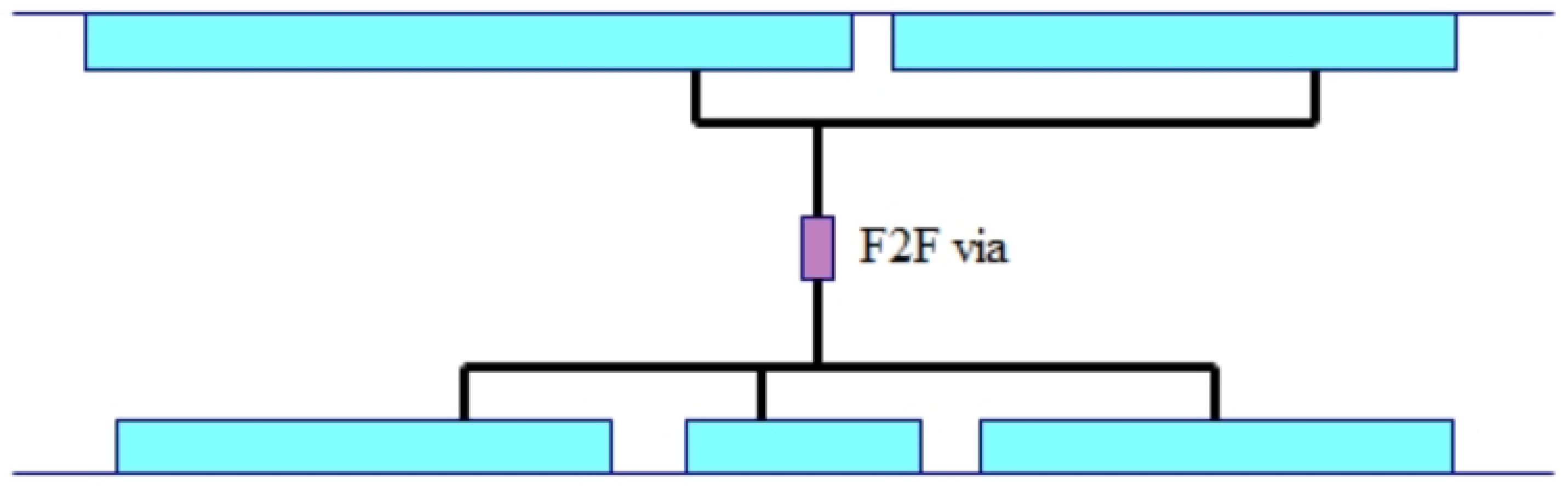
  • Minimize via count. In 3D IC with F2F stacking, the number of layers is 2 ( l = 2 ). If a net spans both two layers, it requires an ITV.
  • Minimize Half-Perimeter Wirelength (HPWL). HPWL model [11] is the most commonly used approximation for evaluating circuit wirelength. Its expression is as follows:
    HPWL = n e t j ( x m a x x m i n ) + ( y m a x y m i n ) ,
    where x m a x denotes the maximum x-coordinates of all the pins involved in a net, and similar meanings apply to x m i n , y m i n , and  y m a x .
Figure 2 shows the concept of the HPWL model. Assume a net consists of four blocks: m, n, k, and p, where m, n are on the first layer, and k, p are on the second layer. According to the block coordinates, we construct the corresponding bounding box of each net as shown by the dashed lines. The HPWL of the net equals ( x p x m ) + ( y p y m ) .
In order to represent 3D structures of floorplans, researchers have employed various approaches, with some utilizing an array of 2D representations to depict 3D structures for 3D floorplanning purposes. Examples include the multi-layer BSG (Bounded Slice-line Grid) [27] and Partitioned Sequence Pair [28], where each 2D representation corresponds to a floorplan of a single tier. Alternatively, other researchers have extended existing 2D representations to represent genuine 3D structures. For instance, Yamazaki et al. [29] employed the sequence three times, Cheng et al. [30] utilized the 3D slicing tree, and Ma et al. [31] introduced 3D-CBL (Corner Block List) for encoding 3D structure topologies. However, these authentic 3D representations lead to a significant increase in the number of possible floorplan configurations, resulting in a high degree of redundancy that undermines efficiency. In this paper, P-SP is adopted as the representation for the floorplan structure.
P-SP is an extension of the well-studied sequence pairs [11] used to represent 2D floorplans. An SP can be represented as a tuple ( X , Y ) , where X and Y are two ordered sequences. In general, the sequence pair imposes the following relationships between each pair of blocks:
( < b i b j > , < b i b j > ) b i is left to b j ,
( < b j b i > , < b i b j > ) b i is below b j .
Given an SP, the block packing can be computed by applying the well-known longest path algorithm for the vertex-weighted directed acyclic graph [11]. Its computational time complexity is O ( n 2 ) . Later, Tang et al. [32] proposed a fast longest common subsequence algorithm, which reduces the time complexity of transforming SP into a planar graph to O ( n log log n ) . Therefore, we adopt the latter.
One sequence pair can generate multiple partitioned sequence pairs, and each sub-sequence pair in the P-SP represents a floorplan of the corresponding layer. The difference is that the number of blocks in these sub-sequence pairs is variable. An example of the P-SP is shown in Figure 3. Specifically, for the floorplanning of two layers, P-SP contains 2 sets of sequence pairs: ( X 1 , Y 1 ) , ( X 2 , Y 2 ) .

2.2. Multi-Objective Optimization

MOO is a specialized field dedicated to addressing optimization problems characterized by multiple conflicting objectives [33]. In contrast to traditional single-objective optimization, which focuses on minimizing or maximizing a single objective function, MOO aims to identify a set of solutions that represent a compromise among conflicting objectives.
Let X denote the decision variable space, Y represent the objective space, and  f i : X R denote the i-th objective function. In the context of minimization problems, the following principles are considered:
  • Pareto Dominance. Given two solutions x 1 and x 2 , if  x 1 is at least as good as x 2 in all objectives and strictly better in at least one objective, then x 1 dominates x 2 , denoted as x 1 x 2 . The dominance relation is defined as
    x 1 x 2 i , f i ( x 1 ) f i ( x 2 ) j , f j ( x 1 ) < f j ( x 2 ) .
  • Pareto Front. The Pareto Front (PF) is the set of solutions in the decision variable space that are not dominated by any other solution. This represents a collection of different balanced solutions where no solution is superior in all objectives. It is formally expressed as
    PF = { x X x X , x x } .
  • Diversity and Balance. MOO aims to find a set of solutions that form a balance in the objective space. Let F ( x ) = [ f 1 ( x ) , f 2 ( x ) , . . . , f k ( x ) ] denote the vector of objectives for solution x. The objective is to find a set of non-dominated solutions that are widely distributed in the objective space, representing the Pareto Front.
  • Hypervolume Indicator. For a given set of points P on the Pareto front, the hypervolume indicator HI ( P ; r ) is the Lebesgue measure of the hypervolume covered by all boxes with points from P as upper corners and the reference point r as the lower corner.
  • Methods. Dealing with MOO problems involves various traditional methods, including Pareto-based methods and metaheuristic approaches. MOSA is a heuristic algorithm suitable for MOO problems. Introducing the idea of SA [34] into the field of MOO has led to various approaches of MOSA [35,36,37].
In comparison to single-objective optimization, MOO provides a more comprehensive understanding and balance among multiple objectives, thus improving the overall performance of solutions. Moreover, MOO facilitates the identification of a Pareto front within the design space, resulting in a diverse range of solutions, offering numerous trade-off possibilities, and enhancing flexibility in decision making.

3. Methods

3.1. Objective Function
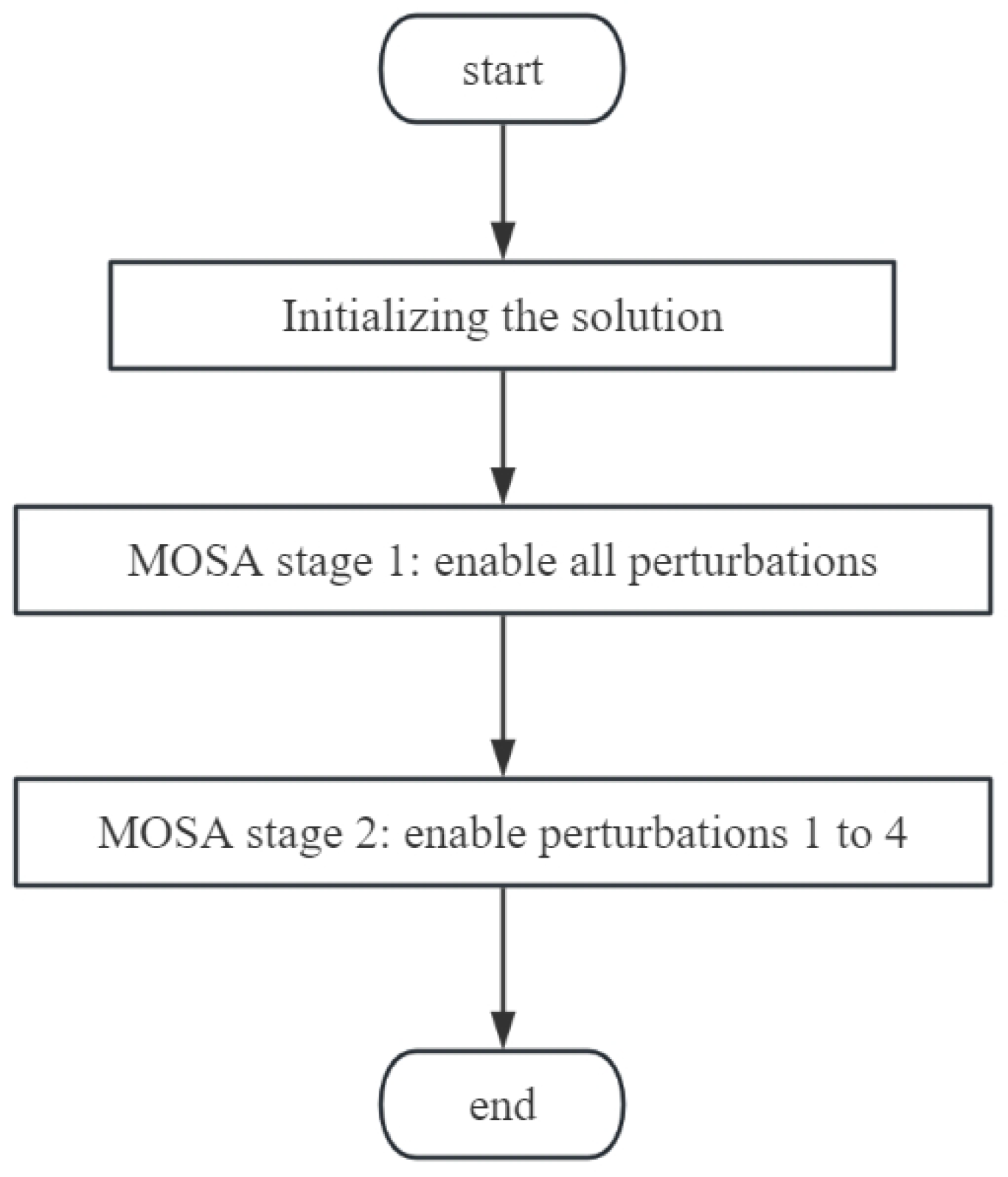
There are four cost functions defined. First, the wirelength cost function directly utilizes the HPWL model [11], so its expression is the same as Equation (1):
min w i r e = n e t j ( x m a x x m i n ) + ( y m a x y m i n ) .
Second, for each layer, an area cost is set, and they are defined using the same method of 2D floorplanning [38]. Thus, the area cost for the t-th layer is represented as
a c t = E W + E H · λ + C 1 · max ( E W , E H · λ ) + C 2 · max ( W t , H t · λ ) ,
in which E W = max ( W t W 0 , 0 ) and E H = max ( H t H 0 , 0 ) represent the excessive width and height of the floorplan. Their visual representation is depicted in Figure 4. W t and H t represent the width and height of the t-th layer floorplan. C 1 and C 2 are user-defined constants, with  C 1 generally greater than C 2 . Drawing from the experience of [38], we set C 1 = 1 and C 2 = 1 / 16 . By employing this formula, we not only penalize excessive width and height but also ensure the effectiveness of the area cost when integrated with other objectives.
In this work, we set the aspect ratio λ to 1.0 and the white space ratio γ to 12%. After computing the area cost for each layer, their average is used to represent the total area cost function:
min a c ¯ = 1 2 ( a c 1 + a c 2 ) .
The average is taken here instead of the maximum because optimization on any layer needs to reflect on the area cost function.
Third, the via cost function is defined as the total number of required ITVs:
min v i a = # I T V .
Fourth, to achieve a good area, the distribution of block areas across layers should be relatively balanced. Therefore, balance cost is necessary as it helps prevent the acceptance of poor layering schemes. We denote the sum of the areas of blocks located on the t-th layer as A t . Then, the balance cost function is defined as follows:
min b a l a n = A 1 A 2 / A .

3.2. Overall Flow

In this paper, heuristic search is used to find the optimal solution. In order to explore a better floorplan, the neighboring solution is generated based on the current solution by a random perturbation. Given the orientation of all blocks and the P-SP as ( X 1 , Y 1 ) , ( X 2 , Y 2 ) , the following five perturbations are defined, including four intra-layer perturbations and one inter-layer perturbation:
  • In any layer t, randomly swap a pair of blocks in either sequence X t or Y t .
  • In any layer t, randomly swap the same pair of blocks in both sequences X t and Y t .
  • In any layer t, randomly select a block and place it in a new position in both sequences X t and Y t .
  • In any layer t, randomly select a block and rotate its orientation by 90 degrees.
  • Select a block in any layer t and place it in a new random position on another layer.
    This is the only type of inter-layer perturbation. To avoid excessively large jumps in a single perturbation, we restrict the selection of blocks within a defined range. We ensure that the increase in ITV count in a single perturbation does not exceed 1 % , and it does not result in A t being less than 0.475 A .
For each perturbation generated, calculations are required, including transforming P-SP into a floorplan and computing the cost function. In the computation of the cost function, the majority of time is spent on calculating the HPWL. Assuming there are m nets in the design, with an average of k pins per net, the time complexity for calculating the semi-perimeter is O ( m k ) . Meanwhile, the time complexity of transforming P-SP into a floorplan is O ( n log log n ) , where n is the number of blocks. Therefore, the time complexity for computing one disturbance is O ( n log log n + m k ) . In the benchmark dataset utilized in this article, it holds that k < 3 .
The overall flow is depicted in Figure 5. For the initial solution, a clustering method called Modified Hyperedge Coarsening (MHEC) [39] is employed for initial layer partitioning, then P-SP and the orientation of all blocks are randomly generated. MHEC is a clustering method. It describes blocks and their connectivity relationships using hypergraphs, allowing closely connected blocks to cluster together and complete the initial layer allocation. After initializing the solution, the MOSA method is applied in two stages. In the first stage, we enable all the perturbations to simultaneously optimize area, wirelength, and ITV count. Good layer partitioning schemes will be discovered during the search process. In the second stage, inter-layer perturbations are disabled, and only intra-layer perturbations are retained. During this stage, the layer partitioning scheme has been determined, and the focus shifts to optimizing area and wirelength.

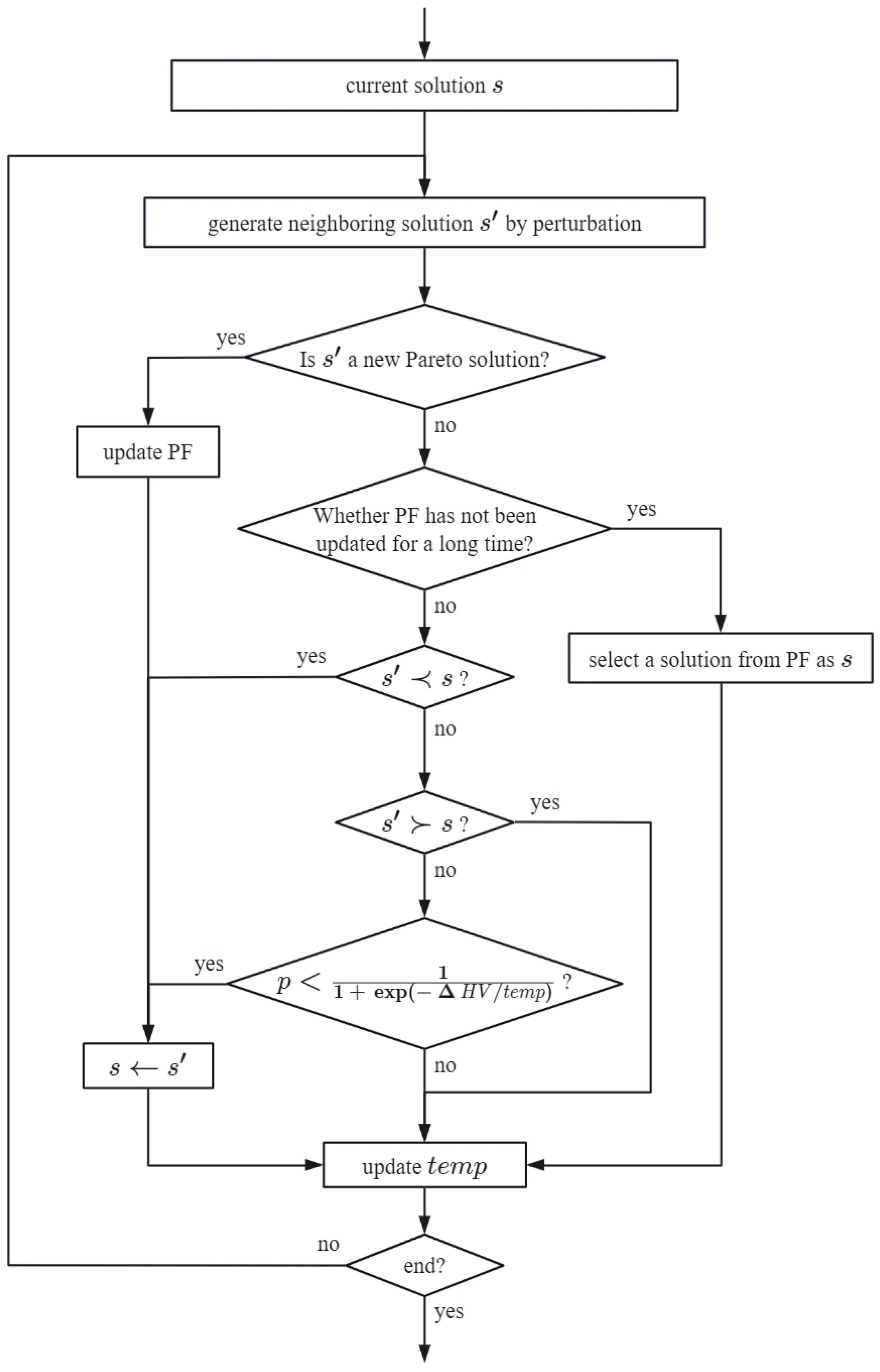
3.3. Multi-Objective Simulated Annealing

After generating neighboring solutions through perturbation, MOSA criteria are employed to determine how to update the solutions. The MOSA setting in this paper is a variant of the setting in [25], primarily selecting various strategies based on the dominance relationship of solutions. This diversity in strategies increases the flexibility of exploring the solution space.
In the decision-making process, if the neighboring solution is a new Pareto solution, it is accepted, thereby updating the PF. Alternatively, if the new solution fails to qualify as a new Pareto solution, three cases are considered based on the dominance relationship between the neighboring solution and the current solution:
  • The neighboring solution dominates the current solution. In this case, the neighboring solution is accepted.
  • The neighboring solution and the current solution are mutually non-dominated. In this case, the neighboring solution is accepted with a probability:
    p = 1 1 + exp ( Δ H V / t e m p ) ,
    where Δ H V represents the hypervolume improvement of the neighboring solution relative to the current solution, and  t e m p represents the annealing temperature, which decreases gradually as the search process progresses. It is similar to a sigma function, where the acceptance probability is 1/2 when Δ H V equals 0, and as Δ H V increases, the acceptance probability also increases. When the temperature is low enough, for  Δ H V greater than 0, the acceptance probability approaches 1, and for Δ H V less than 0, the acceptance probability approaches 0.
  • The neighboring solution is dominated by the current solution. In this case, the neighboring solution is refused.
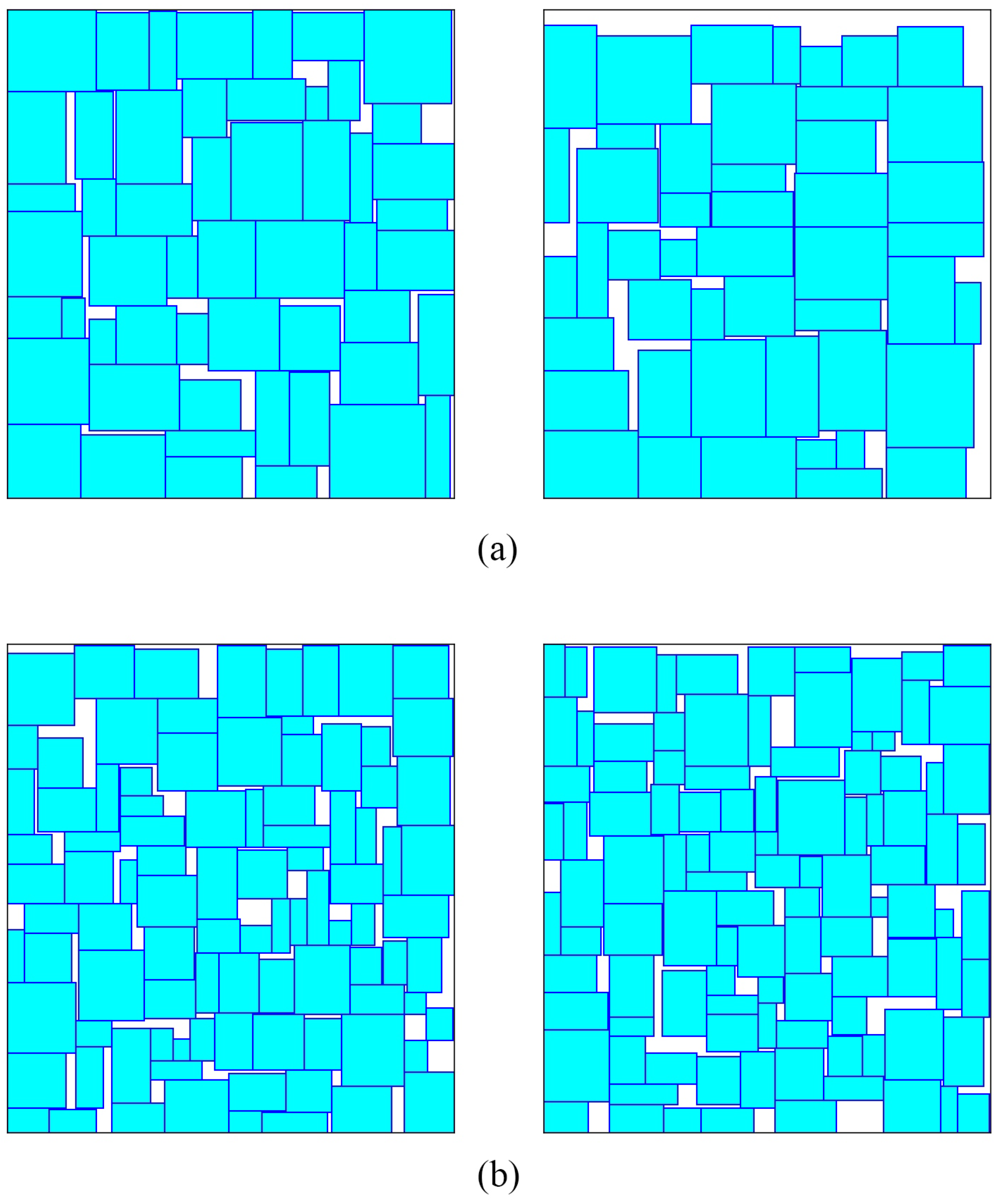
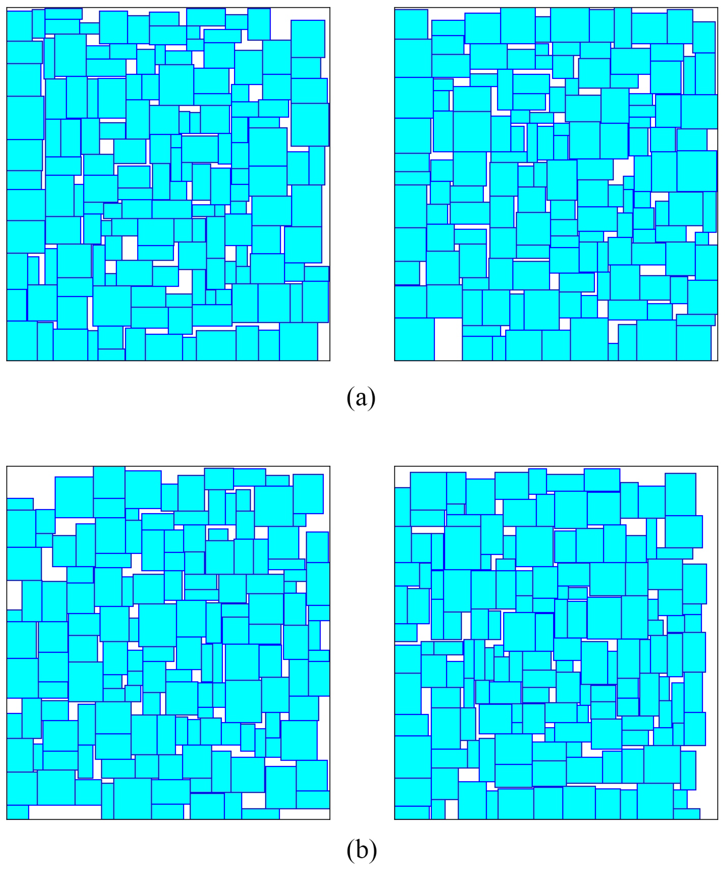
Furthermore, in the event that the PF remains unchanged for a long time, a randomly chosen solution from the PF is updated as the current solution. The entire MOSA process is illustrated in Figure 6.
Next, we introduce the definition of the hypervolume improvement Δ H V . To facilitate the computation of hypervolume, normalize all the four cost functions, obtaining four maximization objectives:
A c = W 0 a c ¯ , W i r e = m ( W 0 + H 0 ) w i r e ,
V i a = m v i a m , B a l a n = 1 b a l a n ,
where m is the number of nets. This normalization method transforms all minimization costs into maximization objectives. Among them, area and wirelength cost are normalized in inverse proportion, amplifying the change in costs at lower states. It is beneficial for exploring higher quality solutions when the solution is good.
For a given solution s, the hypervolume H V ( s ; r ) is defined as the Lebesgue measure of the hyper-volume covered by the box with point s as upper corners and the reference point r as the lower corner. Especially, choosing the origin as the reference point r, then H V ( s ; r ) can be represented as
H V s = A c W i r e V i a B a l a n .
H V is expressed as the product of every objective. It is fair to each objective, and the improvement rate of any objective is directly reflected in H V . Geometrically, H V is a high-dimensional feature of the four objectives, which collects information from all objectives without relying on the adjustment of weights.
Then, the improvement of H V from the current solution to the neighboring solution can be defined as
Δ H V = H V n e i g h b o r i n g H V c u r r e n t .
Obviously, when the neighboring solution dominates the current solution, Δ H V > 0 ; when the current solution dominates the neighboring solution, Δ H V < 0 .

4. Results

In the field of 3D floorplanning, we use the commonly used [13,14,18,19] three benchmark datasets in public available GSRC benchmark: n100, n200, and n300. The comprehensive details of these datasets are elaborated on in Table 1. During the computation of HPWL, all terminals are projected to the edges of the floorplan, ensuring their placement at the minimum Manhattan distance position.
In our method, using n to represent the number of blocks, the steps for the first MOSA stage is set as n 200 , where inter-layer perturbations account for approximately 1 / 5 . And the search steps for the second MOSA stage are set as n 1000 . In the experiments, our method achieved a 100% success rate in satisfying the fixed-outline constraint and obtained favorable area and wirelength. The visualization of the test results on n100 and n200 is shown in Figure 7.
Next, we will compare our test results with those of other similar methods. Firstly, to demonstrate the superiority of 3D floorplanning, we present the test results of the MOSA method in a 2D floorplanning work [25], which shares similar MOSA criteria with our work but does not consider layering factors, focusing solely on optimizing area and wirelength. Note that this is for single-layer floorplanning, which means l = 1 . Additionally, the maximum white space rate γ is set to 10%. We name this method as “2D-MOO”.
Additionally, we implement a single-objective optimization 3D floorplanning method [16]. In this method, the overall cost is described as the weighted sum of specific cost functions, and a single-objective SA method is used for the heuristic search. The heuristic search process is also divided into two stages, but they separate layer allocation from area and wirelength optimization. In the first stage, they only optimize via count and area balance, while in the second stage, they optimize area and wirelength. For fair comparison, the search steps in the first stage are set to n 40 , roughly equivalent to the number of inter-layer perturbations in our method. Additionally, the search steps in the second stage are set to n 1160 to ensure that the total number of search steps is equal. We chose this method for comparison because both our method and this method are two-stage heuristic search methods, and both use P-SP to represent floorplans. The difference lies in its use of single-objective optimization and the separate optimization of layer assignment from the optimization of area and wirelength. It helps to underscore the value of the contributions made in this paper. We name this method as “3D-SOO” (3D Single-Objective Optimization).
Finally, we implement a multi-objective optimization scheme with priority layer partitioning. In this scheme, a hypergraph partitioning tool, hMETIS [40], is used to generate the initial layer allocation scheme. The hMETIS tool implements a hypergraph partitioning method and is a commonly used open-source partitioning tool in the circuit domain. It can find high-quality partitioning schemes without violating area balance, ensuring minimal connectivity between different partitions. In addition to replacing the initial layering with the hMETIS tool, the first MOSA stage is also eliminated, and the search steps in the second stage are set to n 1160 , roughly equivalent to the total number of intra-layer perturbations in our method. We name this method “3D-MOOHL” (3D MOO hMETIS Layering).
We name our original method “3D-MOOFP” (3D MOO Floorplanning). All the detailed test results are shown in Table 2, in which “Succ” denotes the success rate in satisfying the fixed-outline constraint, and HPWL is measured in micrometers (μm). All results are obtained by averaging the outcomes of 10 independent test runs.
When setting fixed-outline, the maximum white space rate γ for single-layer 2D floorplanning is 10%, while for double-layer 3D floorplanning, it is set at 12%. Therefore, compared to 2D floorplanning, 3D floorplanning optimizes approximately 49% area. Furthermore, all 3D methods achieved better wirelength compared to 2D methods. Specifically, 3D-MOOFP showed an average improvement of approximately 21%.
The 3D-SOO [16] performs overall worse in all three optimization objectives compared to the other two 3D methods. In terms of success rate, only n100 achieves 100%. Regarding wirelength, it lags behind across the board. In terms of via count, only n100 is better than 3D-MOOHL, and only n300 is better than 3D-MOOFP. In comparison with 3D-SOO [16], our 3D-MOOFP achieves an average improvement of about 3% in wirelength and achieves the success rate of 100% for n200 and n300 datasets in terms of area. The visual comparison of tests on n300 is shown in Figure 8. It is evident that there is less empty space in our method.
The 3D-MOOHL performs as well as 3D-MOOFP in terms of area, achieving a 100% success rate. However, it slightly lags behind 3D-MOOFP in terms of wirelength optimization. Regarding via optimization, it outperforms 3D-MOOFP overall, only slightly underperforming on the n100 dataset.
In summary, 3D-MOOFP exhibits the most outstanding overall performance. Our method has achieved a success rate of 100% in 3D floorplanning and is leading in optimizing wirelength. Additionally, it also exhibited the best performance in via count optimization for the n100 dataset.

5. Discussion and Conclusions

We have conducted the following analysis of the test results:
  • Due to the 3D stacking technology, 3D approaches have achieved significant advancements in both area and wirelength optimization compared to the 2D method [25].
  • Compared to 3D-SOO [16], 3D-MOOFP leads across all objectives overall, benefiting from the advantages of multi-objective optimization. It only falls behind in optimizing via count for n300, which might be attributed to sacrifices made for area and wirelength optimization.
  • Compared to 3D-MOOHL, 3D-MOOFP excels across all objectives in wirelength optimization. It benefits from the synergistic optimization of all objectives in the first MOSA stage. When employing the hMETIS [40] tool for layer partitioning, it is restricted to optimizing via count solely under the condition of relatively balanced area, without taking into account the potential impact of this partitioning scheme on area and wirelength. In contrast, our approach enables the consideration of all optimization objectives simultaneously. This allows us to identify layer partitioning schemes that are more conducive to wirelength optimization.
  • In terms of via count optimization, the performance difference between the 3D-MOOFP and 3D-MOOHL methods is quite noticeable. It may be attributed to fundamental differences in the partitioning approach. In 3D-MOOHL, a professional partitioning tool is for layer assignment, which may be more proficient in via count optimization. In 3D-MOOFP, layer assignment is explored step by step through a heuristic approach, hence it performs well only on datasets with simpler structures. For the entire floorplanning approach, we provide an effective approach.
In conclusion, we introduce a method that simultaneously conducts layer partitioning and multi-objective collaborative optimization during the optimization process to address the F2F 3D floorplanning problem. We explore neighboring solutions by intra-layer or inter-layer perturbations and then determine strategies based on the dominance relationship of solutions, achieving synergistic optimization of area, wirelength, and ITV count. The test results on the publicly available GSRC benchmark demonstrate that our method effectively addresses the 3D floorplanning problem. Multi-objective optimization facilitates synergistic optimization among objectives, leading to excellent solutions.

Author Contributions

Conceptualization, Z.Y.; methodology, Z.Y. and Z.J.; software, Z.J.; validation, Z.J.; formal analysis, Z.Y. and Z.J.; investigation, Z.Y. and Z.J.; resources, Z.L.; data curation, Z.J.; writing—original draft preparation, Z.J.; writing—review and editing, Z.Y. and Z.J.; visualization, Z.J.; supervision, Z.L.; project administration, Z.L.; funding acquisition, Z.L. All authors have read and agreed to the published version of the manuscript.

Funding

The Strategic Priority Research Program of the Chinese Academy of Sciences (XDA0330401), CAS Youth Interdisciplinary Team (JCTD-2022-07).

Data Availability Statement

The data presented in this study are available in this article.

Conflicts of Interest

The authors declare no conflicts of interest.

Abbreviations

The following abbreviations are used in this manuscript:
ICIntegrated Circuit
VLSIVery Large Scale Integration
EDAElectronic Design Automation
NPNon-deterministic Polynomial-time
GAGenetic Algorithm
BSGBounded Slice-line Grid
CBLCorner Block List
PFPareto Front
FOFPFixed-Outline Floorplanning
M3DMonolithic 3D Integration
F2FFace-to-Face
TSVThrough Silicon Via
ITVInter-Tier Via
MIVMonolithic Integrated Vias
HPWLHalf Perimeter Wirelength
SPSequence Pairs
P-SPPartitioned Sequence Pairs
SASimulated Annealing
MOOMulti-Objective Optimization
MOSAMulti-Objective Simulated Annealing
MHECModified Hyperedge Coarsening
SOOSingle-Objective Optimization
MOOHLMulti-Objective Optimization hMETIS Layering
MOOFPMulti-Objective Optimization Floorplanning

References

  1. Souri, S.J.; Banerjee, K.; Mehrotra, A.; Saraswat, K.C. Multiple Si layer ICs: Motivation, performance analysis, and design implications. In Proceedings of the 37th Annual Design Automation Conference, Los Angeles, CA, USA, 5–9 June 2000; pp. 213–220. [Google Scholar]
  2. Joyner, J.W.; Zarkesh-Ha, P.; Meindl, J.D. A global interconnect design window for a three-dimensional system-on-a-chip. In Proceedings of the IEEE 2001 International Interconnect Technology Conference (Cat. No. 01EX461), Burlingame, CA, USA, 6 June 2001; IEEE: Piscataway, NJ, USA, 2001; pp. 154–156. [Google Scholar]
  3. Vanna-Iampikul, P.; Shao, C.; Lu, Y.C.; Pentapati, S.; Lim, S.K. Snap-3D: A constrained placement-driven physical design methodology for face-to-face-bonded 3D ICs. In Proceedings of the 2021 International Symposium on Physical Design, Virtual, 22–24 March 2021; pp. 39–46. [Google Scholar]
  4. Lim, S.K. 3D-MAPS: 3D massively parallel processor with stacked memory. In Design for High Performance, Low Power, and Reliable 3D Integrated Circuits; Springer: New York, NY, USA, 2013; pp. 537–560. [Google Scholar]
  5. Gomes, W.; Khushu, S.; Ingerly, D.B.; Stover, P.N.; Chowdhury, N.I.; O’Mahony, F.; Balankutty, A.; Dolev, N.; Dixon, M.G.; Jiang, L.; et al. 8.1 Lakefield and Mobility Compute: A 3D Stacked 10 nm and 22FFL Hybrid Processor System in 12× 12 mm 2, 1 mm Package-on-Package. In Proceedings of the 2020 IEEE International Solid-State Circuits Conference-(ISSCC), San Francisco, CA, USA, 16–20 February 2020; IEEE: Piscataway, NJ, USA, 2020; pp. 144–146. [Google Scholar]
  6. Hu, K.S.; Chi, H.Y.; Lin, I.J.; Wu, Y.H.; Chen, W.H.; Hsieh, Y.T. 2023 ICCAD CAD Contest Problem B: 3D Placement with Macros. In Proceedings of the 2023 IEEE/ACM International Conference on Computer Aided Design (ICCAD), San Francisco, CA, USA, 29 October–2 November 2023; IEEE: Piscataway, NJ, USA, 2023; pp. 1–6. [Google Scholar]
  7. Otten, R.H. What is a floorplan? In Proceedings of the 2000 International Symposium on Physical Design, San Diego, CA, USA, 9–12 April 2000; pp. 201–206. [Google Scholar]
  8. Chen, T.C.; Chang, Y.W. Modern floorplanning based on B/sup*/-tree and fast simulated annealing. IEEE Trans. Comput.-Aided Des. Integr. Circuits Syst. 2006, 25, 637–650. [Google Scholar] [CrossRef]
  9. Kahng, A.B. Classical floorplanning harmful? In Proceedings of the 2000 International Symposium on Physical Design, San Diego, CA, USA, 9–12 April 2000; pp. 207–213. [Google Scholar]
  10. Adya, S.N.; Markov, I.L. Fixed-outline floorplanning: Enabling hierarchical design. IEEE Trans. Very Large Scale Integr. (VLSI) Syst. 2003, 11, 1120–1135. [Google Scholar] [CrossRef]
  11. Murata, H.; Fujiyoshi, K.; Nakatake, S.; Kajitani, Y. VLSI module placement based on rectangle-packing by the sequence-pair. IEEE Trans. Comput.-Aided Des. Integr. Circuits Syst. 1996, 15, 1518–1524. [Google Scholar] [CrossRef]
  12. Frantz, F.; Labrak, L.; O’Connor, I. 3D-IC floorplanning: Applying meta-optimization to improve performance. In Proceedings of the 2011 IEEE/IFIP 19th International Conference on VLSI and System-on-Chip, Kowloon, Hong Kong, 3–5 October 2011; IEEE: Piscataway, NJ, USA, 2011; pp. 404–409. [Google Scholar]
  13. Chen, S.; Yoshimura, T. Multi-layer floorplanning for stacked ICs: Configuration number and fixed-outline constraints. Integration 2010, 43, 378–388. [Google Scholar] [CrossRef]
  14. Xu, Q.; Chen, S.; Li, B. Combining the ant system algorithm and simulated annealing for 3D/2D fixed-outline floorplanning. Appl. Soft Comput. 2016, 40, 150–160. [Google Scholar] [CrossRef]
  15. Guler, A.; Jha, N.K. Hybrid monolithic 3-D IC floorplanner. IEEE Trans. Very Large Scale Integr. (VLSI) Syst. 2018, 26, 1868–1880. [Google Scholar] [CrossRef]
  16. Zhu, H.Y.; Zhang, M.S.; He, Y.F.; Huang, Y.H. Floorplanning for 3D-IC with Through-Silicon via co-design using simulated annealing. In Proceedings of the 2018 IEEE International Symposium on Electromagnetic Compatibility and 2018 IEEE Asia-Pacific Symposium on Electromagnetic Compatibility (EMC/APEMC), Singapore, 14–18 May 2018; IEEE: Piscataway, NJ, USA, 2018; pp. 550–553. [Google Scholar]
  17. Shanthi, J.; Rani, D.G.N.; Rajaram, S. Thermal Aware Floorplanner for Multi-Layer ICs with Fixed-Outline Constraints. In Proceedings of the 2021 2nd International Conference on Communication, Computing and Industry 4.0 (C2I4), Bangalore, India, 16–17 December 2021; IEEE: Piscataway, NJ, USA, 2021; pp. 1–6. [Google Scholar]
  18. Lin, J.M.; Chang, W.Y.; Hsieh, H.Y.; Shyu, Y.T.; Chang, Y.J.; Lu, J.M. Thermal-aware floorplanning and TSV-planning for mixed-type modules in a fixed-outline 3-D IC. IEEE Trans. Very Large Scale Integr. (VLSI) Syst. 2021, 29, 1652–1664. [Google Scholar] [CrossRef]
  19. Kadambarajan, J.P.; Pothiraj, S.; Kadarkarai, P. GPU Implementation of Thermal Aware 3D IC Floorplanning. Int. J. Comput. Inf. Syst. Ind. Manag. Appl. 2021, 13, 8. [Google Scholar]
  20. Meitei, N.Y.; Baishnab, K.L.; Trivedi, G. Fast power density aware three-dimensional integrated circuit floorplanning for hard macroblocks using best operator combination genetic algorithm. Int. J. Circuit Theory Appl. 2023, 51, 4879–4896. [Google Scholar] [CrossRef]
  21. Guan, W.; Tang, X.; Lu, H.; Zhang, Y.; Zhang, Y. A novel thermal-aware floorplanning and tsv assignment with game theory for fixed-outline 3-D ICs. IEEE Trans. Very Large Scale Integr. (VLSI) Syst. 2023, 31, 1639–1652. [Google Scholar] [CrossRef]
  22. He, Z.; Ma, Y.; Zhang, L.; Liao, P.; Wong, N.; Yu, B.; Wong, M.D. Learn to floorplan through acquisition of effective local search heuristics. In Proceedings of the 2020 IEEE 38th International Conference on Computer Design (ICCD), Hartford, CT, USA, 18–21 October 2020; IEEE: Piscataway, NJ, USA, 2020; pp. 324–331. [Google Scholar]
  23. Xu, Q.; Geng, H.; Chen, S.; Yuan, B.; Zhuo, C.; Kang, Y.; Wen, X. GoodFloorplan: Graph Convolutional Network and Reinforcement Learning-Based Floorplanning. IEEE Trans. Comput.-Aided Des. Integr. Circuits Syst. 2021, 41, 3492–3502. [Google Scholar] [CrossRef]
  24. Amini, M.; Zhang, Z.; Penmetsa, S.; Zhang, Y.; Hao, J.; Liu, W. Generalizable Floorplanner through Corner Block List Representation and Hypergraph Embedding. In Proceedings of the 28th ACM SIGKDD Conference on Knowledge Discovery and Data Mining, Washington, DC, USA, 14–18 August 2022; pp. 2692–2702. [Google Scholar]
  25. Jiang, Z.; Li, Z.; Yao, Z. Multi-Objective Optimization in Fixed-Outline Floorplanning through Reinforcement Learning. Comput. Electr. Eng. 2024. submitted to publication. [Google Scholar]
  26. GSRC Benchmark. Available online: http://vlsicad.eecs.umich.edu/BK/GSRCbench (accessed on 9 October 2023).
  27. Deng, Y.; Maly, W.P. Interconnect characteristics of 2.5-D system integration scheme. In Proceedings of the 2001 International Symposium on Physical Design, Sonoma County, CA, USA, 1–4 April 2001; pp. 171–175. [Google Scholar]
  28. Shiu, P.H.; Ravichandran, R.; Easwar, S.; Lim, S.K. Multi-layer floorplanning for reliable system-on-package. In Proceedings of the 2004 IEEE International Symposium on Circuits and Systems (ISCAS), Vancouver, BC, Canada, 23–26 May 2004; IEEE: Piscataway, NJ, USA, 2004; Volume 5, pp. 69–72. [Google Scholar]
  29. Yamazaki, H.; Sakanushi, K.; Nakatake, S.; Kajitani, Y. The 3D-packing by meta data structure and packing heuristics. IEICE Trans. Fundam. Electron. Commun. Comput. Sci. 2000, 83, 639–645. [Google Scholar]
  30. Cheng, L.; Deng, L.; Wong, M.D. Floorplanning for 3-D VLSI design. In Proceedings of the 2005 Asia and South Pacific Design Automation Conference, Shanghai, China, 18–21 January 2005; pp. 405–411. [Google Scholar]
  31. Ma, Y.; Hong, X.; Dong, S.; Cheng, C. 3D CBL: An efficient algorithm for general 3D packing problems. In Proceedings of the 48th Midwest Symposium on Circuits and Systems, Cincinnati, OH, USA, 7–10 August 2005; IEEE: Piscataway, NJ, USA, 2005; pp. 1079–1082. [Google Scholar]
  32. Tang, X.; Tian, R.; Wong, D. Fast evaluation of sequence pair in block placement by longest common subsequence computation. In Proceedings of the Conference on Design, Automation and Test in Europe, Paris, France, 27–30 March 2000; pp. 106–111. [Google Scholar]
  33. Collette, Y.; Siarry, P. Multiobjective Optimization: Principles and Case Studies; Springer Science & Business Media: Berlin, Germany, 2004. [Google Scholar]
  34. Kirkpatrick, S.; Gelatt, C.D., Jr.; Vecchi, M.P. Optimization by simulated annealing. Science 1983, 220, 671–680. [Google Scholar] [CrossRef] [PubMed]
  35. Ulungu, L.; Teghem, J.; Ost, C. Interactive simulated annealing in a multiobjective framework: Application to an industrial problem. J. Oper. Res. Soc. 1998, 49, 1044–1050. [Google Scholar] [CrossRef]
  36. Suppapitnarm, A.; Seffen, K.A.; Parks, G.T.; Clarkson, P. A simulated annealing algorithm for multiobjective optimization. Eng. Optim. 2000, 33, 59–85. [Google Scholar] [CrossRef]
  37. Suman, B. Study of simulated annealing based algorithms for multiobjective optimization of a constrained problem. Comput. Chem. Eng. 2004, 28, 1849–1871. [Google Scholar] [CrossRef]
  38. Chen, S.; Yoshimura, T. Fixed-outline floorplanning: Block-position enumeration and a new method for calculating area costs. IEEE Trans. Comput.-Aided Des. Integr. Circuits Syst. 2008, 27, 858–871. [Google Scholar] [CrossRef]
  39. Karypis, G.; Aggarwal, R.; Kumar, V.; Shekhar, S. Multilevel hypergraph partitioning: Application in VLSI domain. In Proceedings of the 34th Annual Design Automation Conference, Anaheim, CA, USA, 9–13 June 1997; pp. 526–529. [Google Scholar]
  40. Karypis, G.; Kumar, V. Multilevel k-way hypergraph partitioning. In Proceedings of the 36th Annual ACM/IEEE Design Automation Conference, New Orleans, LA, USA, 21–25 June 1999; pp. 343–348. [Google Scholar]
Figure 1. Face-to-face stacking.
Electronics 13 01696 g001
Figure 2. HPWL model.
Electronics 13 01696 g002
Figure 3. The block position allocation corresponding to the P-SP ( < 1 , 3 , 2 > , < 1 , 2 , 3 > ) , ( < 5 , 4 > , < 4 , 5 > ) .
Electronics 13 01696 g003
Figure 4. Schematic diagrams of excessive width and excessive height.
Electronics 13 01696 g004
Figure 5. Overall flow.
Electronics 13 01696 g005
Figure 6. MOSA process.
Electronics 13 01696 g006
Figure 7. Visualization example of test results on GSRC benchmark. (a) n100; (b) n200.
Electronics 13 01696 g007
Figure 8. The visual comparison of tests on n300. (a) 3D-MOOFP; (b) 3D-SOO.
Electronics 13 01696 g008
Table 1. Benchmarks.
Circuit# Blocks# Terminals# Nets
n100100334885
n2002005641585
n3003005691893
Table 2. Test results.
2D-MOO [25]3D-SOO [16]3D-MOOHL3D-MOOFP
Succ HPWL Succ HPWL #ITV Succ HPWL #ITV Succ HPWL #ITV
n100100%221,576100%180,681145100%175,125150100%173,092141
n200100%405,71270%329,488302100%321,034283100%319,528293
n300100%566,19060%457,464379100%451,628321100%449,872395
Disclaimer/Publisher’s Note: The statements, opinions and data contained in all publications are solely those of the individual author(s) and contributor(s) and not of MDPI and/or the editor(s). MDPI and/or the editor(s) disclaim responsibility for any injury to people or property resulting from any ideas, methods, instructions or products referred to in the content.

