Article

Optimizing CNN Hardware Acceleration with Configurable Vector Units and Feature Layout Strategies

1
AnnLab, Institute of Semiconductors, Chinese Academy of Sciences, Beijing 100083, China
2
College of Materials Science and Opto-Electronic Technology & School of Integrated Circuits, University of Chinese Academy of Sciences, Beijing 100049, China
3
Beijing Key Laboratory of Semiconductor Neural Network Intelligent Sensing and Computing Technology, Beijing 100083, China
*
Author to whom correspondence should be addressed.
Electronics 2024, 13(6), 1050; https://doi.org/10.3390/electronics13061050
Submission received: 7 February 2024 / Revised: 7 March 2024 / Accepted: 8 March 2024 / Published: 12 March 2024

Abstract

:
Convolutional neural network (CNN) hardware acceleration is critical to improve the performance and facilitate the deployment of CNNs in edge applications. Due to its efficiency and simplicity, channel group parallelism has become a popular method for CNN hardware acceleration. However, when processing data involving small channels, there will be a mismatch between feature data and computing units, resulting in a low utilization of the computing units. When processing the middle layer of the convolutional neural network, the mismatch between the feature-usage order and the feature-loading order leads to a low input feature cache hit rate. To address these challenges, this paper proposes an innovative method inspired by data reordering technology, aiming to achieve CNN hardware acceleration that reuses the same multiplier resources. This method focuses on transforming the hardware acceleration process into feature organization, feature block scheduling and allocation, and feature calculation subtasks to ensure the efficient mapping of continuous loading and the calculation of feature data. Specifically, this paper introduces a convolutional algorithm mapping strategy and a configurable vector operation unit to enhance multiplier utilization for different feature map sizes and channel numbers. In addition, an off-chip address mapping and on-chip cache management mechanism is proposed to effectively improve the feature access efficiency and on-chip feature cache hit rate. Furthermore, a configurable feature block scheduling policy is proposed to strike a balance between weight reuse and feature writeback pressure. Experimental results demonstrate the effectiveness of this method. When using 512 multipliers and accelerating VGG16 at 100 MHz, the actual computing performance reaches 102.3 giga operations per second (GOPS). Compared with other CNN hardware acceleration methods, the average computing array utilization is as high as 99.88% and the computing density is higher.

1. Introduction

In recent years, convolutional neural networks (CNNs) have made remarkable achievements in numerous fields, including image classification [1], object detection [2], and stereo vision [3], among others. However, CNNs still face some challenges regarding mobile devices [4,5], due to their computationally intensive and frequent memory access needs.
Currently, accelerator design faces two main challenges: the mapping mechanism between convolutional layers and computation unit arrays, and the storage system with continuous data input. The mapping mechanism aims to improve the utilization of computational resources by correctly mapping the computation layers onto the computation array. However, in [6,7,8,9,10,11], the same computation array is used to process different convolutional layers, resulting in a mismatch between feature formats and computation arrays [12,13], and leading to the underutilization of computational resources. In [14], multiple sets of computation units are designed to match different convolutional layer structures, but the actual performance falls short of expectations due to the difficulty of balancing the computational workload. The storage system largely determines the upper limit of the accelerator’s efficiency. When input data cannot be provided in a timely manner, the computation units must frequently enter idle states, resulting in low work efficiency.
Although accelerators have made some progress in terms of throughput, there is still a significant gap between the theoretical throughput and the actual throughput of hardware accelerators. In a study [15], an accelerator operated at a frequency of 165 MHz, consuming 256 multipliers, with a theoretical throughput of 66.93 GOPS, but the actual throughput only reached 79.52% of the theoretical value. Another accelerator in a different study [16] operated at a frequency of 1 GHz, consuming 512 multipliers, with a theoretical throughput of 498.6 GOPS, but the actual throughput only accounted for 48.69% of the theoretical value. Similar phenomena have also been reflected in other research [17,18,19,20]. In essence, low actual throughput reflects a low utilization efficiency of the multiplier.
This study proposes a novel hardware accelerator for CNN which improves the utilization efficiency of the multiplier through configurable vector units, feature mapping strategies, and feature block scheduling. The main innovations and contributions of this paper are as follows:
  • In order to address the issue of the low utilization efficiency of the computation units when processing large images and small channels, a configurable vector computation unit is proposed. This unit allows for the dynamic adjustment of the hardware structure based on specific task requirements, thereby improving flexibility.
  • To solve the problem of mismatch between feature loading order and feature usage order, a novel off-chip layout strategy based on feature data width grouping is proposed. This strategy effectively improves the burst access efficiency of the feature data and on-chip feature cache hit rate, enabling the more efficient utilization of hardware resources.
  • An adjustable feature block computation scheduling strategy is proposed, which not only serves as a means to adjust weight reuse and feature write-back pressure, but also has great potential in the parallel processing of computational tasks.
The rest of this paper is organized as follows. Section 2 focuses on the descriptions of feature organization, feature block scheduling and distribution, feature computation flow, and the proposed hardware architecture design, emphasizing how the hardware units collaborate to accomplish the aforementioned tasks. Section 3 discusses the experimental design and verification results. Section 4 provides a summary of this paper.

2. Related Work

Currently, the majority of FPGA-based hardware accelerators for CNN primarily use either a single-convolutional layer engine architecture [6,7,8,9,10,11] or a multi-convolutional layer engine architecture [21,22,23,24] to process convolutional layers. The core components of these architectures include a convolutional processing module, which consists of a convolutional layer engine, input buffer, output buffer, external memory, and controller. This design is typically based on loop partitioning and loop unrolling techniques. In a single convolutional layer engine architecture, all convolutional layers are processed by the same convolutional layer engine, and the loop unrolling parameters for each convolutional layer are required to be consistent. However, due to different dimensional requirements for optimal loop unrolling parameters in different convolutional layers, this consistency limits the efficient utilization of computational resources. On the other hand, a multi-convolutional layer architecture includes multiple independent convolutional computation modules, external memory, and controllers. The design intention is to improve the parallel processing capability and overall efficiency of the accelerator by assigning dedicated convolutional computation modules to each convolutional layer. Unlike the layer-wise computation approach in a single convolutional layer engine architecture, the multi-convolutional layer engine architecture can simultaneously process different convolutional layers. However, this requires effective coordination between layers to avoid potential data congestion issues. To achieve inter-layer coordination, some designs introduce handshake mechanisms [14]. While this method simplifies the coordination process, it may also result in a partial redundancy of computational resources.
Previous research has focused on achieving higher parallel processing capability by searching for optimal loop unrolling parameters for each convolutional layer, maximizing the loop unrolling parameters for input and output channels. However, it is difficult to find a unified set of input and output channel loop unrolling factors for all convolutional layers when prioritizing the maximization of loop unrolling factors. If we lower the priority of maximizing loop unrolling factors and instead prioritize finding a unified set of input and output channel loop unrolling parameters for all convolutional layers, it becomes easier to find such parameters. For example, in VGG16, the input channel loop unrolling parameter is 8 and the output channel loop unrolling parameter is 64. We can consider the input channel loop unrolling parameter of 8 to also satisfy the first layer when it is 1 or 3, and further research will be conducted in this regard. As a result, we have a set of loop unrolling parameters that can be applied to all convolutional layers, meaning that a computation array designed according to this set of loop parameters can achieve high utilization in all convolutional layers. However, this may lead to lower throughput. When using feature block scheduling, the computation tasks of a layer can be allocated to multiple identical convolutional engine instances through block task allocation. This method allows for improved throughput not only by increasing the parallel processing of input and output channels but also by distributing computation tasks and running multiple identical convolutional engine instances simultaneously, resulting in more efficient computation. This block scheduling strategy can effectively utilize computational resources, optimize the allocation of computation tasks, and improve the overall system performance.
Therefore, the motivation of this study is to improve computational efficiency while maintaining good throughput performance by sharing the same computational unit in convolutional layers with different scale parameters, combined with effective data organization and feature block scheduling methods. It is worth noting that, for the sake of simplicity, we focused on studying how to reuse the same computational unit in each convolutional layer of VGG16 while maintaining good computational efficiency. This paper does not address the further parallel acceleration of the same convolutional layer by expanding multiple identical convolutional layer computation units. This focus helps to gain a deeper understanding of how to achieve the sharing of computational units in specific convolutional structures and provides a clear foundation for subsequent research and applications.

3. The Proposed Methods

3.1. Overview of Optimization Strategies

To tackle the problem of low cache hit rates caused by mismatched feature loading and computation order in general feature arrangement schemes, we introduce the concept of feature groups. To address the issue of low utilization of computation arrays in large images with small channels during channel group parallel acceleration, we propose the use of configurable vector units for mode switching.

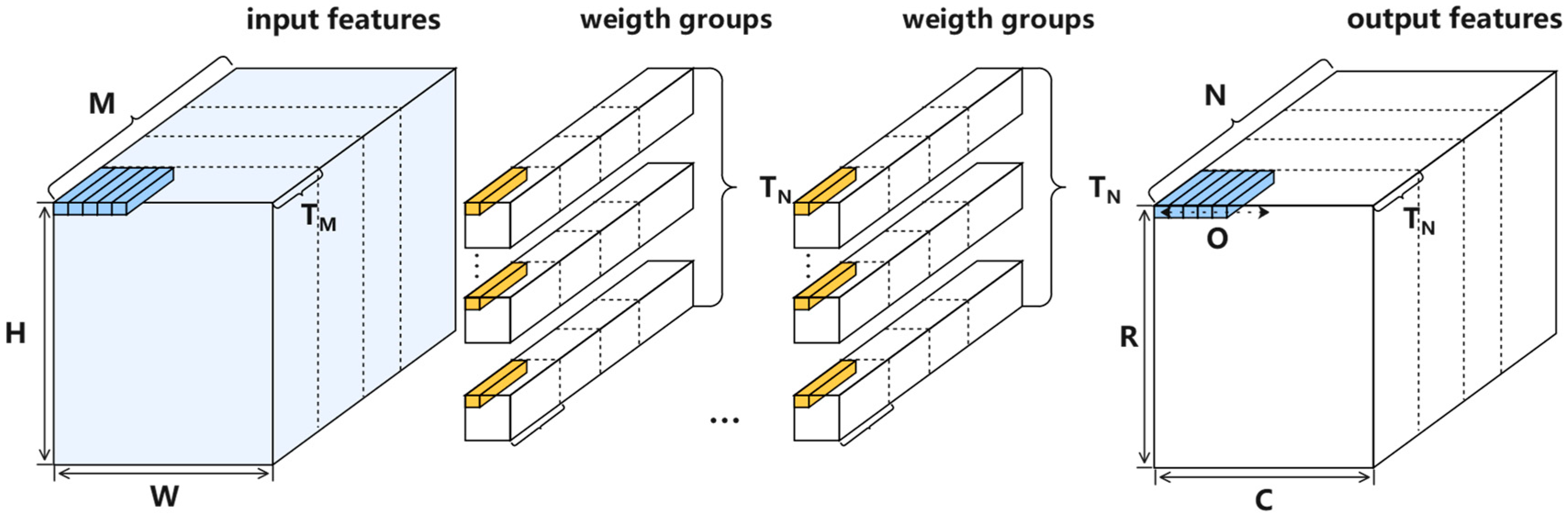
3.1.1. Mapping of Computation with Feature Group Constraints

In the design of CNN hardware accelerators, the computation mapping strategy [25,26,27] plays a crucial role in achieving improved performance, energy efficiency, and real-time capabilities. Carefully designed computation mapping schemes enhance hardware utilization by efficiently utilizing computational capabilities during CNN task execution. This not only reduces the time required for inference but also provides stronger computational support for applications in resource-constrained environments. As illustrated in Figure 1, the parallelization factor for feature input channels is denoted as T M , and for feature output channels as T N . The input feature data are divided into M / T M channel groups, and the output data into N / T N input channel groups. The output channels correspond to the weights, meaning that the weights are also divided into N / T N weight groups. The number of channels in the last group may be less than T M or T N , and any insufficient parts are filled with zero values to ensure data regularity and calculation accuracy. Within each input channel group, O sets of T M -length data are sequentially input into the multiplication array, where O represents the maximum computation block width. Each layer consists of (R × C)/O computation blocks. When the plane convolution calculation for O output feature points is completed, the computation for this channel group concludes, and the computation for the next input channel group begins, until all M / T M input channel groups have been calculated.
If the sub-convolutions after splitting are directly input into the multiplication array for sequential computation, performing convolution on a per-channel group basis would increase the pressure on the output cache. Additionally, it would require writing the intermediate results into the external memory and then reading them back for accumulation, which adds complexity and wastes memory bandwidth. To address this, we can perform convolution on a per-computation block basis within the channel group. The convolution results of each computation block can then be submitted to the cache, with each computation block’s result being cached separately.
The traditional computation mapping strategy, which focuses on channel group parallelism for acceleration, achieves the highest input feature reuse rate only when a sufficiently large maximum computation width is utilized, spanning multiple rows and aligning with the beginning and end of rows. However, the effectiveness of this approach is limited by the fact that different network layers exhibit significant variations in feature map sizes. For instance, while some layers may have relatively small feature maps, others may have much larger ones. Consequently, a fixed maximum computation width cannot maintain stable input feature utilization efficiency across different network feature map sizes. In other words, typical CNN hardware acceleration computation mapping strategies suffer from low input feature cache loading hit rates due to these disparities.
Based on the preceding analysis, we propose the computation mapping strategy depicted in Figure 2. The feature map width is partitioned into Y feature groups based on T C . At this stage, we define O as the product of T R and T C , where T R signifies the output feature height block size and T C denotes the output feature width block size. Introducing the concept of feature groups into the feature layout enables the setting of a sufficiently large value for O, free from constraints imposed by excessively large feature map widths. This alleviates the issue of loading a large amount of input features without effective utilization, thereby enhancing input feature utilization efficiency across different network layers. During feature block grouping, the weights corresponding to each feature block group remain constant, while the input and output channel groups of the features persist. The feature data are rearranged within the feature block group to enhance memory access efficiency.

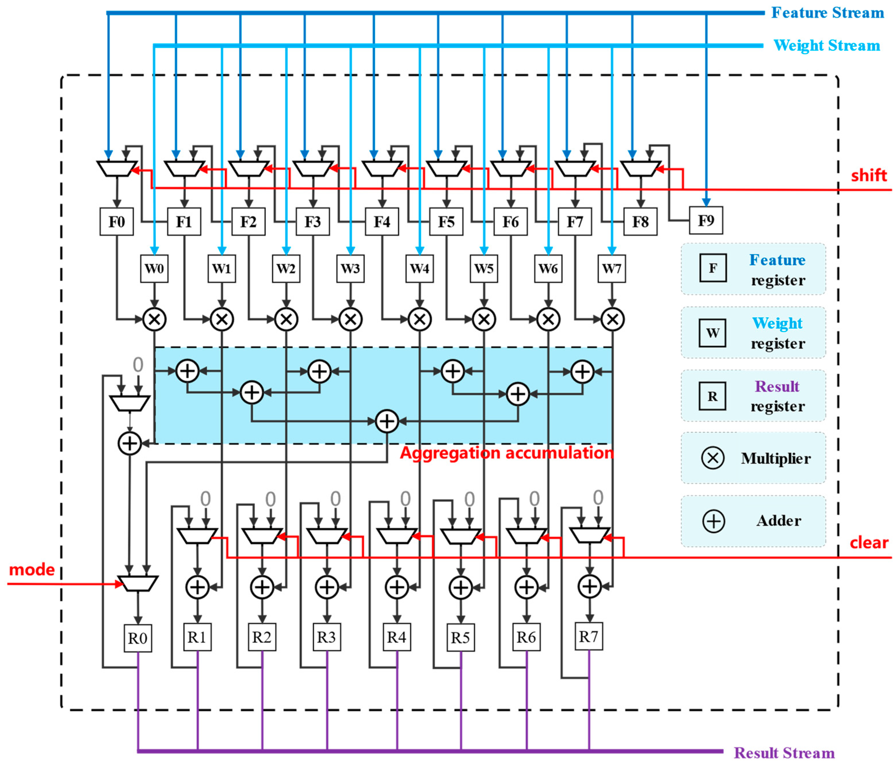
3.1.2. Configurable Vector Unit

The above reasoning is based on the assumption that the input feature data points are arranged continuously within the input channel, where the size of an input channel group is T M . For an input feature point at the spatial position index (h, w), there are T M consecutive points along the input channel direction. However, due to the characteristics of large input feature maps and small channels in the first layer, the input channels are usually 1 or 3, which means that only 1 or 3 out of the T M consecutive points are valid. Therefore, the utilization efficiency of the multiplication array of size T M × T N is not as high as 3/ T M for each T M multiplier. Hence, it is necessary to map the computational resources to the spatial convolution. Since the first layer convolutional layer often has a large feature map size, there are enough computational operations for the multiplication array calculation. In this case, the computating array needs to be transformed, where T M multiplication units are configured as a vector computation unit. By controlling the accumulation method, it can support the parallel computation of multiple output feature points or a single output feature point simultaneously, i.e., calculating T M output feature points in a batch or just one output feature point.
When conducting 2D convolution with T M = 1 , the multiplication operations corresponding to T C output feature points are decomposed onto the multiplication units, as depicted in Figure 3a. Conversely, when the input channels are sufficiently large and no 2D convolution is performed, the multiplication operations in the input channel direction are mapped onto the multiplication units, as illustrated in Figure 3b.
Two computation mapping strategies correspond to two different formats of off-chip feature arrangement. The utilization of different feature arrangement formats aims to enhance the compatibility with the computation array. In output feature rearrangement, the channel direction holds the highest priority, facilitating flexible feature loading by rows and ensuring the efficient processing of overlapping feature data during block scheduling in the height direction. The scale of the output feature submission cache remains consistent across both working modes. When computing the same output channel group, identical weight parameters are reused through batch operations to generate T R × T C × T N output feature data. By continuously alternating the calculation of the output channel group, T R × T C × N output features are produced.
To implement the aforementioned ideas, in the next section, we will elaborate on our proposed design from three aspects: feature organization, feature block scheduling and distribution, and feature computation.

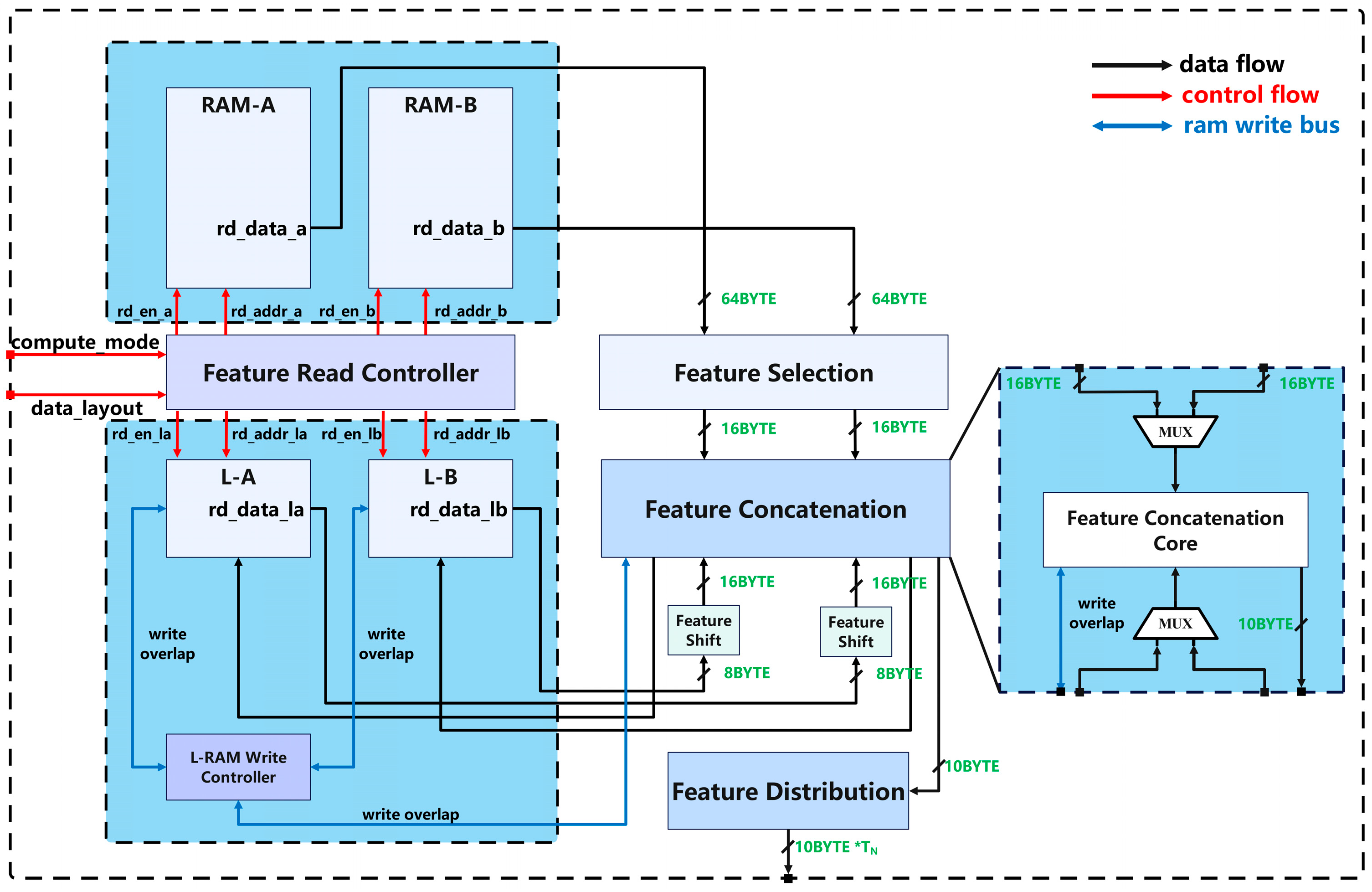
3.2. Feature Organization

Based on the computation mapping strategies and feature grouping layout method we have proposed, feature organization [28,29] is a major focus and challenge in our work. The goal of feature organization is to enhance the efficiency of feature data processing and ensure that the feature data distribution format aligns perfectly with the configurable vector units. Its significance can be observed in the following three aspects:
  • First, organizing off-chip features into a format that matches the configurable vector units based on the computation mapping strategies;
  • Second, designing on-chip feature caches to support various feature format organizations, thereby improving the efficiency of feature selection and concatenation during feature distribution;
  • Third, achieving complete alignment between the feature distribution format and the configurable vector units through flexible on-chip addressing for on-chip feature selection and concatenation.
The following section will introduce how features are organized, both on-chip and off-chip.

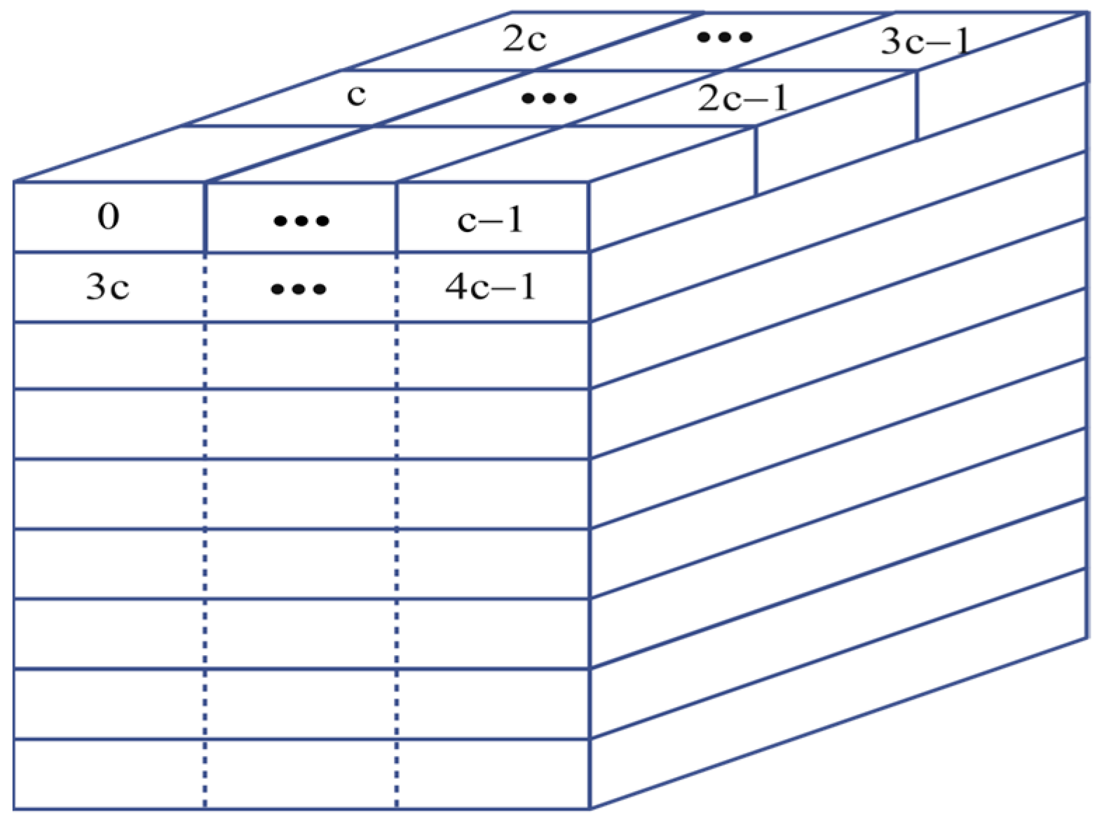
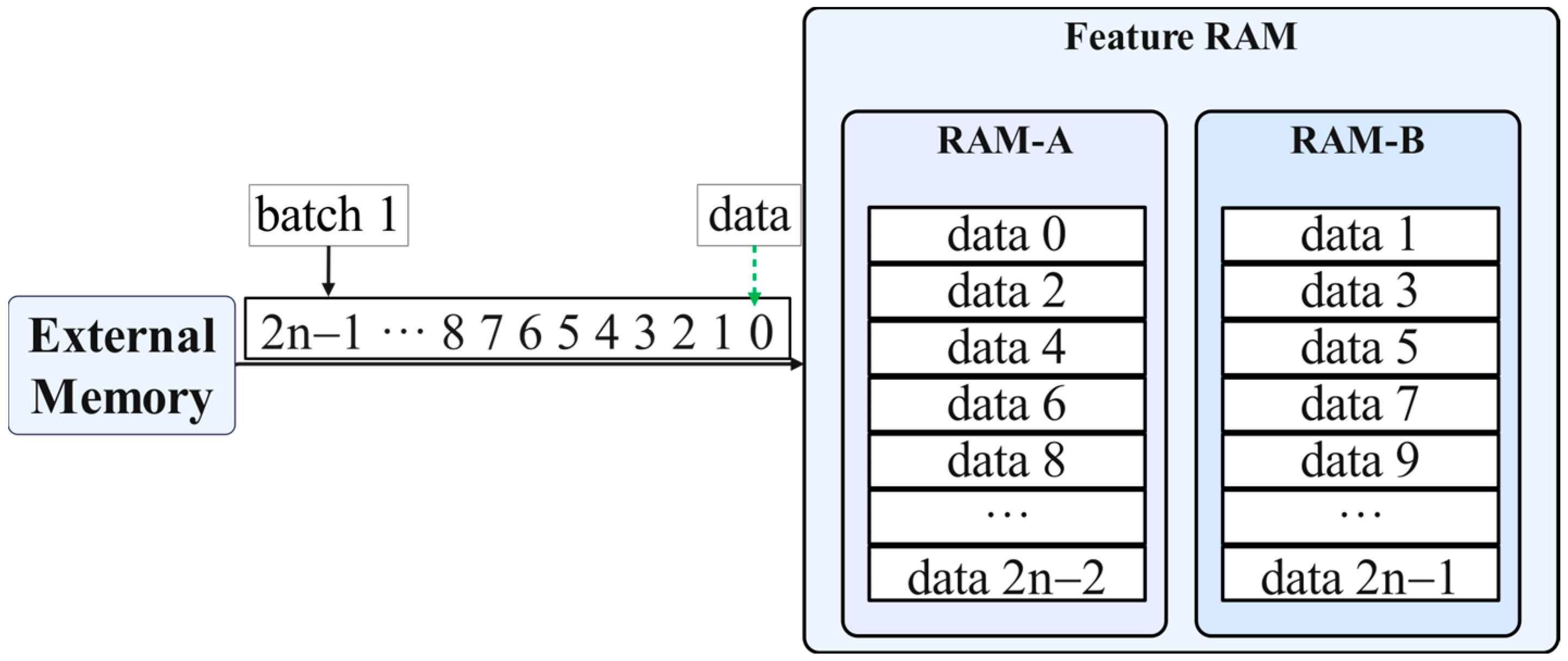
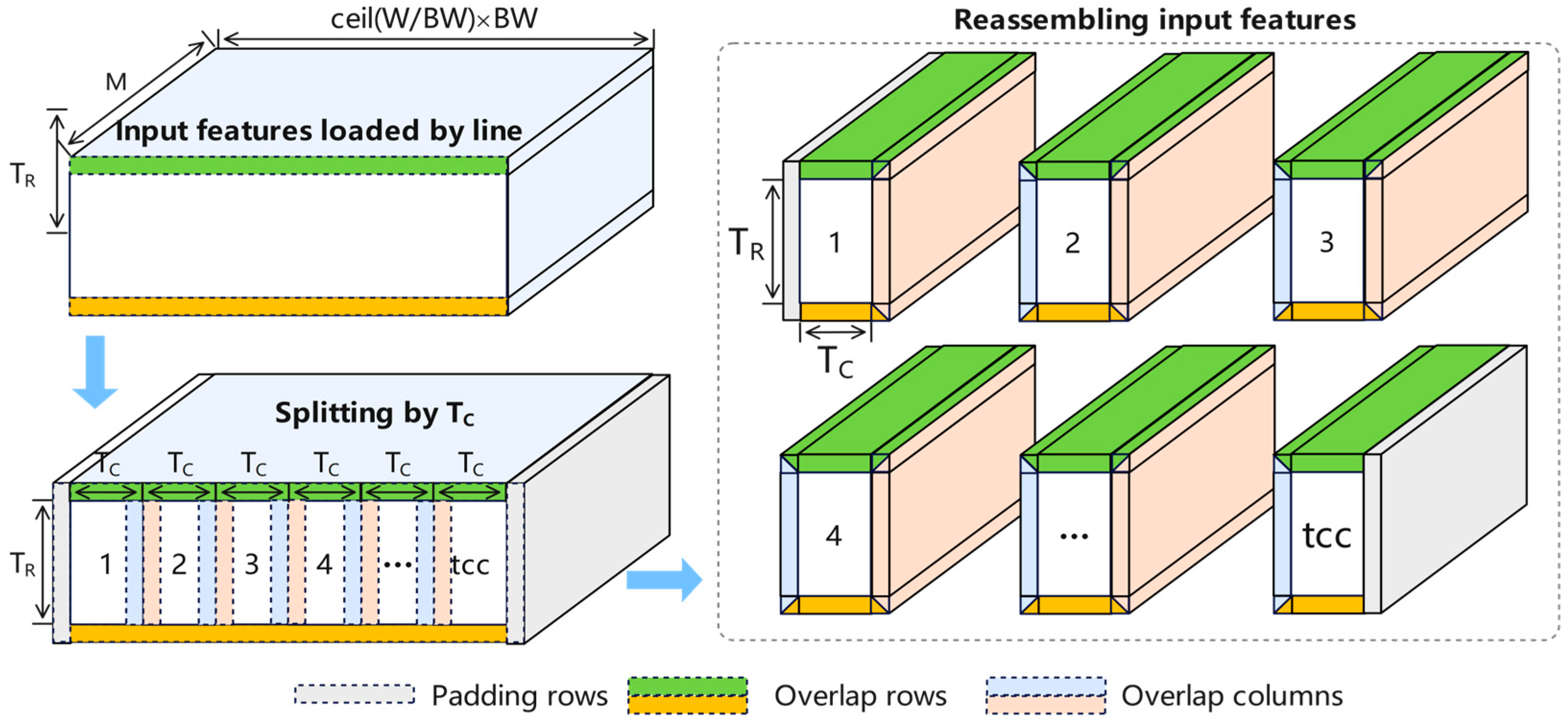
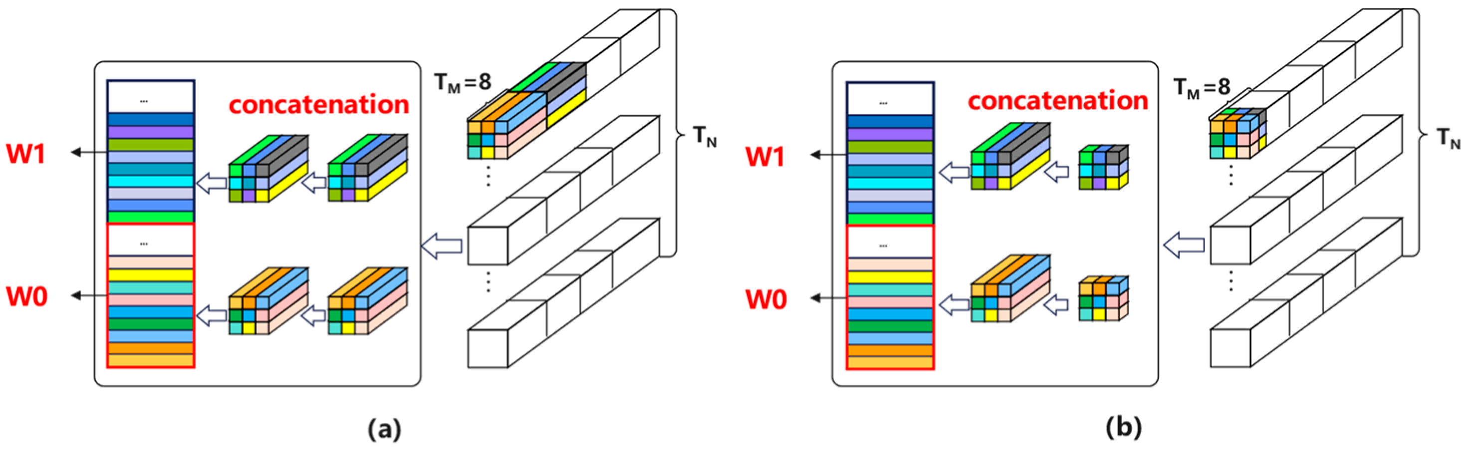
3.2.1. Off-Chip Feature Organization

Off-chip feature data address mapping refers to the technique of storing feature data slices generated by a CNN on a specific physical address in an off-chip storage device. This mapping process allows for effective management and access to feature data, making it a core method for off-chip feature organization. For most intermediate layers of the network, the data format of the feature map width direction grouping, called G C · R T C M , can be expressed as (C//Tc, R, Tc, M//64, M% BW); // means division, and BW is an abbreviation for bus bit width. Figure 4 is an address mapping in G C · R T C M data format, where m represents the number of times M is divisible by BW, and m = ceil (M/BW). When employing the RMC feature layout method, the feature memory access features encompass the ability to burst read all input channel data for any row of feature points and the capability to burst read multiple rows, with each row containing ceil (C/BW) input channel data for feature points.
The address mapping method of the G C · R T C M format is not suitable for processing the input channel of the first layer input feature as 1 or 3. Considering that the first layer usually has a large feature map width and height but fewer input channels, and considering the transmission efficiency and the convenience of addressing when splicing on-chip features, in order to facilitate good matching of data organization and configurable vector units, a new data format called RMC is defined which can be expressed as (R, M, C//BW, C%BW). Figure 5 is an address mapping in RMC data format. Each line of the input feature is aligned to BW bytes, where c represents the number of times the feature map width C is divisible by BW, c = ceil (C/BW). When utilizing the G C · R T C M feature layout method, the feature memory access attribute enables the continuous burst reading of all input channel data of a single feature point. It supports the burst reading of input channel data for consecutive T C feature points in one row and also facilitates burst reading of multiple rows, with each row containing all input channel data of T C feature points.

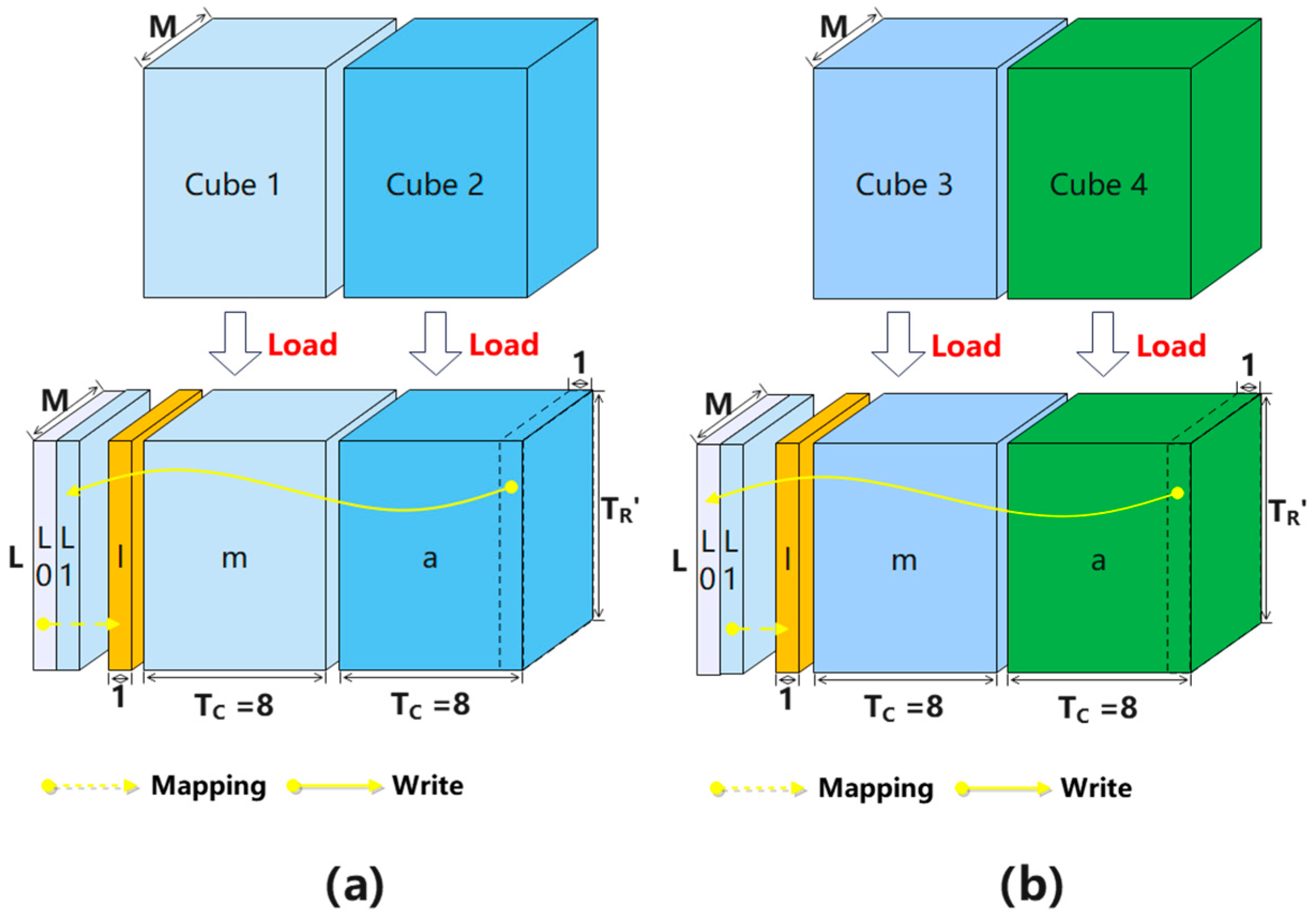
3.2.2. Feature Cache Array Design

The feature cache design is one of the key innovations in this architecture, proposing a unified feature cache design that effectively utilizes the on-chip feature cache space and maximizes the utilization of bus resources for different convolution sizes and strides under different feature layout formats. Due to the grouping of output features in the width direction, organizing the input features well under Gc·RTcM is considered crucial. Therefore, a feature cache design is first proposed to manage the input feature cache with K = 3 and S = 1/2, reducing the redundant loading of overlapping input feature data in the width direction of different output feature blocks. Then, on this basis, support for the RMC format is achieved through on-chip address mapping. This section first introduces how the feature cache is designed for the Gc·RTcM scenario. Firstly, the output feature width is represented by T C and the input feature width is represented by T C according to Equation (1).
T C = ( T C 1 ) × S + K
According to the location of the output feature block, the existence relationship is as follows:
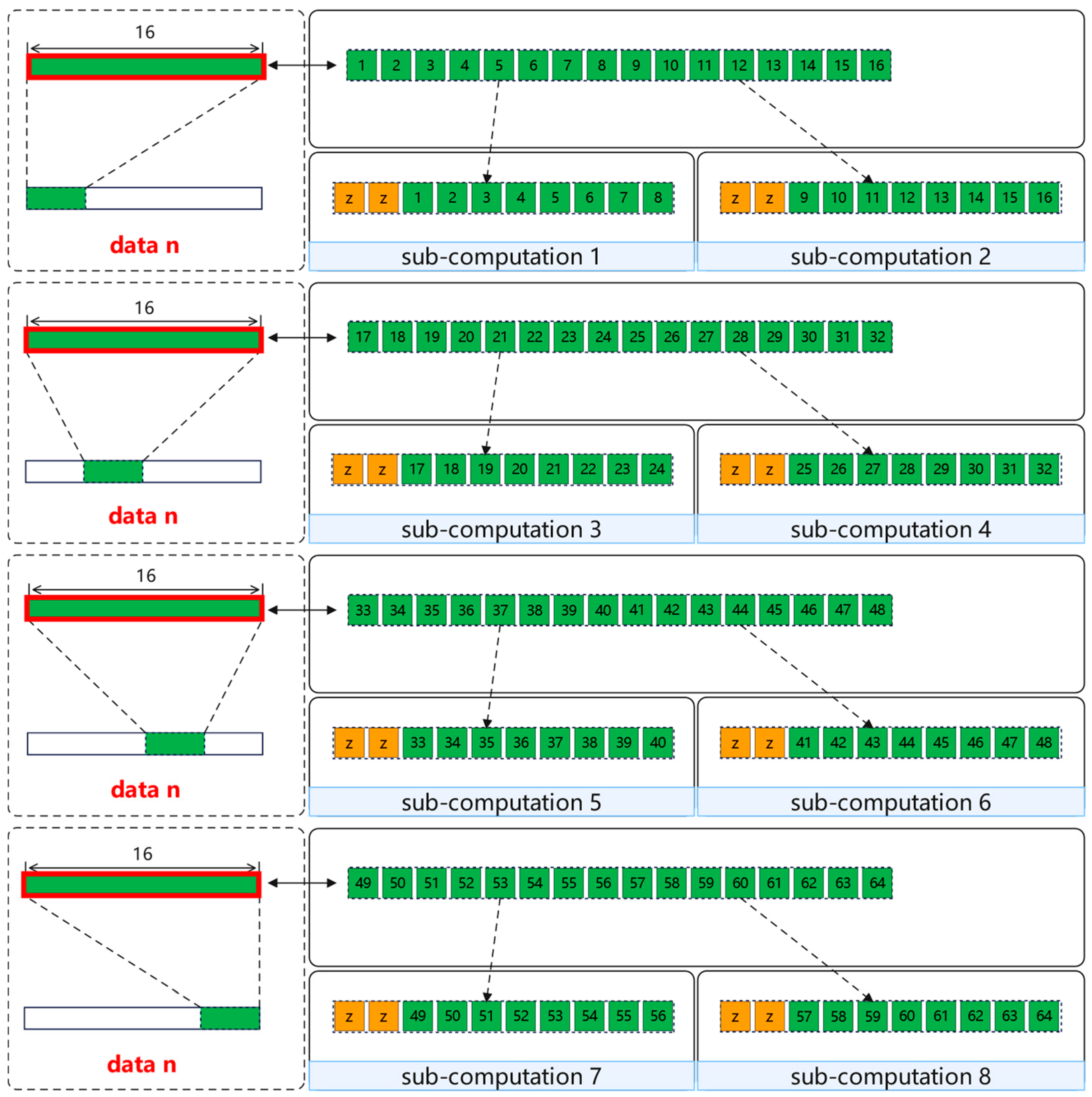
  • Assuming that the output feature points calculated in the current calculation chunk contain the first feature point of a row, the real padding points can be used instead of 1 input feature point;
  • Assuming that the output feature points calculated in the current calculation chunk do not contain the first and last feature points of a row, the real padding points cannot be utilized at this time, and the cached data points are used instead of 1 input feature point;
  • Assuming that the output feature points calculated by the current calculation chunk contain the last feature point of a row, the real padding points can be used instead of 1 input feature point.
  • When utilizing data from real padding points and cached data points, the effective input feature width T C is expressed as Equation (2).
    T C = ( T C 1 ) × S + K 1
When the convolution kernel size K = 3 and the convolution step size S = 1 , at this time the effective input feature width T C = 9 , the regular T C × T R × M feature block is used, and the organization of input feature cache is expressed in Equation (3).
T C × T R × M = 8 × T R × M + ( 1 × T R × M )
The loading feature chunks are shown in Figure 6. First, the feature chunks of Cube1 and Cube2 are loaded. Then, the effective data chunks and the small cache (denoted by l) are selected and merged to form an input feature of size 10 × T R × M , which is used to calculate an output feature of size T C × T R × N . In this process, the roles of the main cube (denoted by m) and the aid cube (denoted by a) are determined based on the size of the effective data. The main cube has a larger effective data size, while the aid cube has a smaller effective data size. Mapping represents the address mapping, and Write represents the actual write operations that write data into the specified space. For example, as shown in Figure 6a, during the computation process, the writing of a portion of the data from data chunk m to L1 space is an actual write operation. In the data organization stage, it can be selected to map the l cache data to L0 space. After completing the computation and outputting the features using Cube1 and Cube2 feature chunks as the main data, the space occupied by Cube1 feature chunk is released, Cube3 feature chunk is loaded, and a new relationship between the main cube and the aid cube is generated. At this point, as shown in Figure 6b, the small cache l is mapped to L1 space, and a portion of the data from data chunk m is written to L0 space.
When the convolution kernel size K = 3 and the convolution stride S = 2 , the effective input feature width T C = 16 . Due to the use of regular T C × T R × M feature chunks, the organization of the input feature cache is expressed in Equation (4).
T C × T R × M = 8 × T R × M + ( 8 × T R × M )
The loading of feature chunks is illustrated in Figure 7. Cube 1 and Cube 2 feature chunks are loaded sequentially, and a portion of the data from data chunk a are written into the L1 space. At the same time, the data cached in l are mapped to the L0 space, as shown in Figure 7a. After the calculation and output of the feature using Cube 1 and Cube 2 as the main data have been completed, the space occupied by Cube 1 and Cube 2 feature chunks is released. Then, Cube 3 and Cube 4 feature chunks are loaded. According to the illustration in Figure 7b, the small cache l is mapped to the L0 space, while a portion of the data from data chunk a is written into the L1 space.
Therefore, the basic structure of the on-chip feature cache array is a small random-access memory (RAM) used to cache historical feature data, and two feature group RAMs used to cache input features of size T C × T R × M . Let L represent the small RAM, and A and B represent the RAMs storing the feature group data. The constructed feature cache array is shown in Figure 8. In this array, L(0–3) stores the overlapping part of the feature blocks in the C direction, and A(0–1) and B(0–1) represent different partitions of the corresponding feature group RAMs. According to the previous analysis of the usage of one-dimensional convolutional feature data, when the stride is 1, alternating between A0 and B0 is sufficient to meet the input feature requirements, while when the stride is 2, one block operation consumes two blocks of feature group data. Therefore, in order to ensure an uninterrupted supply of feature data, the presence of A1 and B1 is required to form a double buffer.
Using the aforementioned feature cache design, on-chip features with different convolution sizes and strides can be achieved under the Gc·RTcM feature layout format.

3.2.3. On-Chip Feature Organization

Feature concatenation is necessary to ensure that the feature distribution format matches the computation array completely. In order to improve the efficiency of feature selection and concatenation during feature distribution, address mapping on feature data slices is crucial.
According to the characteristics of RMC, it is necessary to simultaneously obtain feature data for two adjacent addresses. According to the design of the feature cache, the feature data with consecutive addresses obtained from external storage are alternately mapped to RAM-A and RAM-B, as shown in Figure 9.
According to the characteristics of G C · R T C M features, data concatenation requires the use of feature data from adjacent feature groups. Based on the scheduling algorithm, these feature data are loaded into different storage areas of the on-chip feature cache in two bursts. According to the scheduling algorithm, only one depth of input feature is needed at a time. According to the definition of the feature cache, the feature data with consecutive addresses obtained from external storage need to be mapped in two bursts to RAM-A and RAM-B, respectively, as shown in Figure 10.

3.3. Feature Chunk Scheduling and Distribution

Usually, the bandwidth and on-chip cache pressure can be reduced by using chunked computation. The scheduling of the middle layer of the network adopts the G C · R T C M format, so when the size of the T C value is determined, the output feature width slicing factor is then fixed, and the size of the chunked computation output feature map is T R × T C × N , and the corresponding size of the input features should be T R × T C × N , as shown in Figure 11.
The scheduler determines the timing of the feature loading and feature distribution based on these rules. The previous section introduced the design of an on-chip feature cache based on the basic characteristics of feature group layout, and implemented efficient on-chip addressing for two types of off-chip feature layout. In this section, we will discuss the timing of feature loading and releasing, as well as how to make full use of the feature data already loaded into the on-chip feature cache through feature chunk scheduling. Specifically, we will explore how to correctly select and concatenate data to match the distributed feature data with the data required by the computation array.

3.3.1. R M C Format

When dealing with the RMC format, the spatial combinations to which the partitions of the feature cache can be mapped are A0|B0, A1|B1. Once the feature data for each spatial combination are ready, the computation can start to be initiated, so each spatial combination corresponds to one computation mode, as shown in Figure 12.
The control logic for loading features and starting computation in RMC format is shown in Figure 13. In the figure, load_start controls the initiation of the feature loading request, and load_done indicates the completion of feature loading when there are no available feature spaces for loading. compute_start controls the start of a new computation block, and when the feature cache-ready data satisfy the space combination described above, the feature distribution for the new computation block begins. compute_done indicates the completion of the current computation block, allowing for the release of feature spaces and the efficient utilization of on-chip cache and data bandwidth.
For RMC format features, the number of input feature rows to be loaded by row is determined according to T R to handle padding rows and overlap rows correctly. The feature distribution is performed by selectively splicing the loaded input feature data and dividing the output feature width direction into tcc sub-computations according to T C . t c c denotes the number of output feature width direction chunks according to T C , t c c = c e i l ( C / T C ), as shown in Figure 14.
When dealing with RMC format feature distribution, when T C = 8 if 17 input features points are obtained, the calculation for the case K = 3 and S = 2 can be completed. As shown in Figure 15, where data n − 1, data n and data n + 1 denote the input features of BW bytes of adjacent addresses and the selected feature data are indicated by bold-colored boxes.
Since the feature distribution bus bit width is T N × 10 bytes, the 17 bytes of input feature data are split into two input features of 10 byte size, where z denotes zero and o denotes overlap, as shown in Figure 16.
When T C = 8 , if 10 input feature points are obtained, the calculation can be made for the case of K = 3 and S = 1 . Therefore, similarly, by selecting two pieces of neighboring 16-byte length data, a portion of the data is selected for splicing, as shown in Figure 17.
Since the 16-byte length data can be distributed twice for sub-computation, the selected input data need further processing before they become the final spliced data, where o denotes the overlap taken from the L-cache, as shown in Figure 18.

3.3.2. G C · R T C M Format

For the G C · R T C M format feature with K = 3 and S = 1 , the input feature data consists of the L-cache space and two blocks of feature group data. Under the main/aid switching iteration mode, the feature group data can be mapped to the spatial combinations of A0|B0, B0|A1, A1|B1, and B1|A0. Once the feature data for each spatial combination are ready, the calculation can be initiated. Therefore, each spatial combination corresponds to a computation mode, as shown in Figure 19.
The control logic for loading features and initiating computation in the G C · R T C M format is depicted in Figure 20. In the diagram, load_start controls the initiation of the feature loading request, while load_done indicates the completion of feature loading. When there is no available feature space for loading, it waits for the release of feature space. compute_start controls the start of new computation blocks. When the feature cache-ready data satisfy the aforementioned spatial combination, the distribution of new computation blocks begins. compute_done indicates the completion of the current computation block, allowing for the release of feature space, effectively utilizing the cache and data bandwidth on the chip.
When the total number of calculations for height direction partitioning have been determined, the feature groups are continuously loaded and the input feature data are iteratively used. According to the scheduling, the output feature in the width direction is divided into tcc sub-computations according to T C , as shown in Figure 21.
When dealing with the input feature cache after good management of the input features based on scheduling, the channel parallel computational mapping strategy differs from the convolutional algorithm only in that hardware acceleration introduces channel group parallelism. Since the feature cache design has good management of the input feature data, when dealing with the distribution of G C · R T C M format features, it is only necessary to obtain the input feature data for processing based on the address generated by the convolutional algorithm.
Assuming BW = 64 bytes, when T M = 8 , by splitting the input features by 16 bytes length, half of the 16 bytes of data is taken at a time, so the possible splices are shown in Figure 22.
According to the feature distribution process described above, assuming BW = 64 bytes and T M = 8 , the designed feature distribution circuit is shown in Figure 23. In this circuit, feature concatenation is mainly achieved based on different calculation modes and feature layout formats. The overall process is similar to the one described earlier, where two sets of 64-byte data are obtained and transformed into two sets of 16-byte data through feature selection. Then, they enter the core feature concatenation module for concatenation processing. It is worth noting that during the access process in the L cache, the features need to be shifted to maintain consistency in bit width. After the concatenation is completed, the feature data are copied and selectively broadcast based on the configuration parameters of the computation array. This part of the circuit is omitted in the figure.

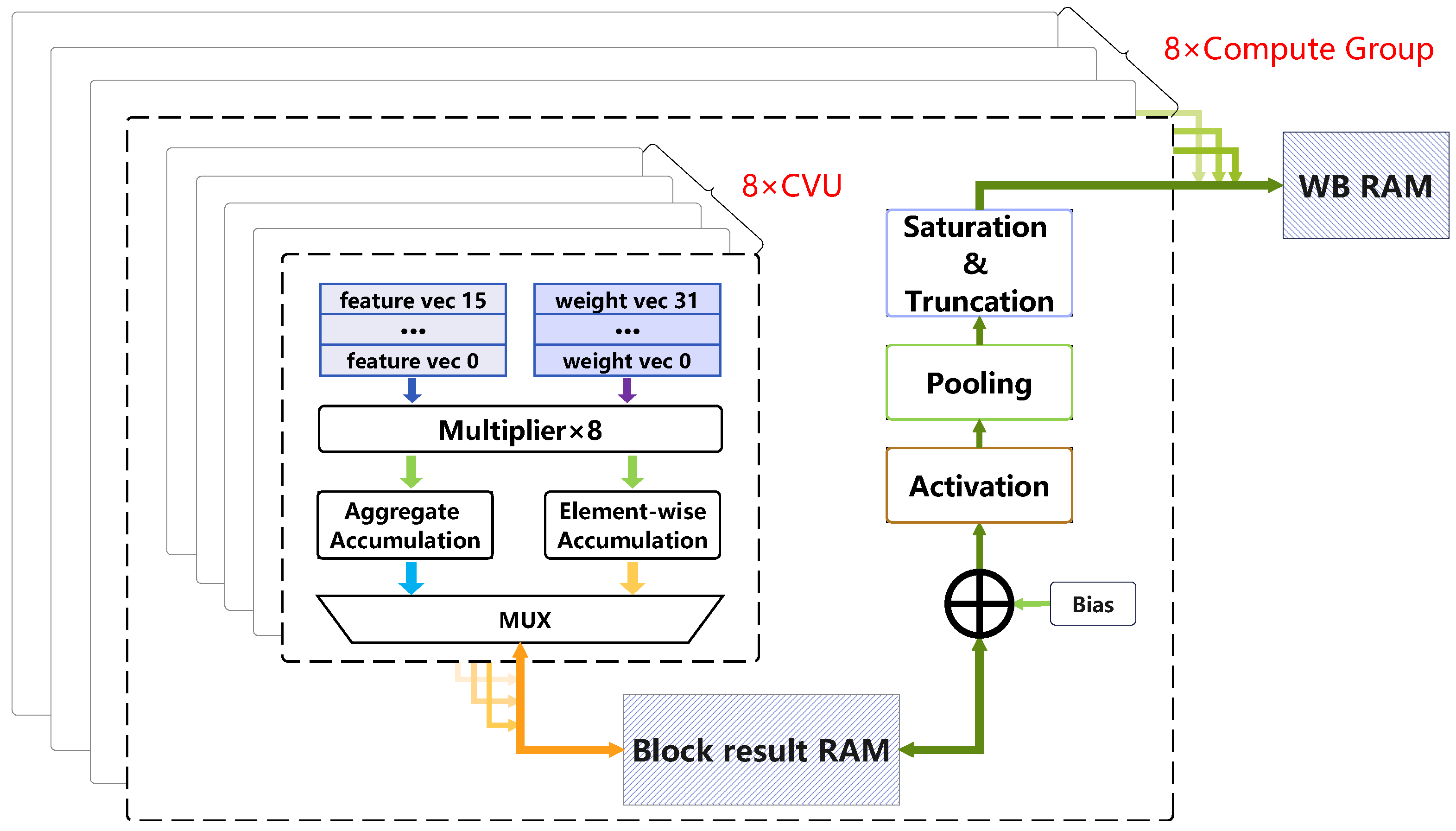
3.4. Feature Computation

To address the issue of utilization efficiency in large graph and small channel computation arrays under conventional multi-channel parallel hardware acceleration strategies, we propose the use of configurable vector units (CVU) as the core units for hardware acceleration. The key feature of these units is the adjustable working mode for accumulation operations, which supports both aggregate accumulation and element-wise accumulation modes. The detailed design of the CVU is shown in Figure 24, where the mode signal controls the selection of accumulation mode, the shift signal controls the shifting of feature data, and the clear signal resets the accumulation result.
After feature distribution, the CVUs now have access to the available feature computation resources. Therefore, feature computation involves correctly utilizing the distributed feature data, including how to match it with the weight data and determine the appropriate vector unit working mode.
If we consider the calculation of weight values corresponding to the current input channel group as a calculation batch, each calculation batch outputs one temporary calculation result and T C temporary calculation results. When T C is equal to 8, the input feature width is 10 bytes, and the input weight width is 8 bytes. By using shifting operations, the input feature data can be expanded and decomposed into multiple sub-operations that interact with the weights.
To match the weight data with the feature data, the weights are rearranged in advance using software to correspond to the input channel groups. During weight distribution, appropriate transformations are applied based on the computation mode. The weights are then distributed to the CVU and stored in the local weight cache. In the G C · R T C M format, the weights remain unchanged, as shown in Figure 25a. In the R M C format, due to the multiplier performing spatial convolution operations, the weights are transformed through replication, as illustrated in Figure 25b.

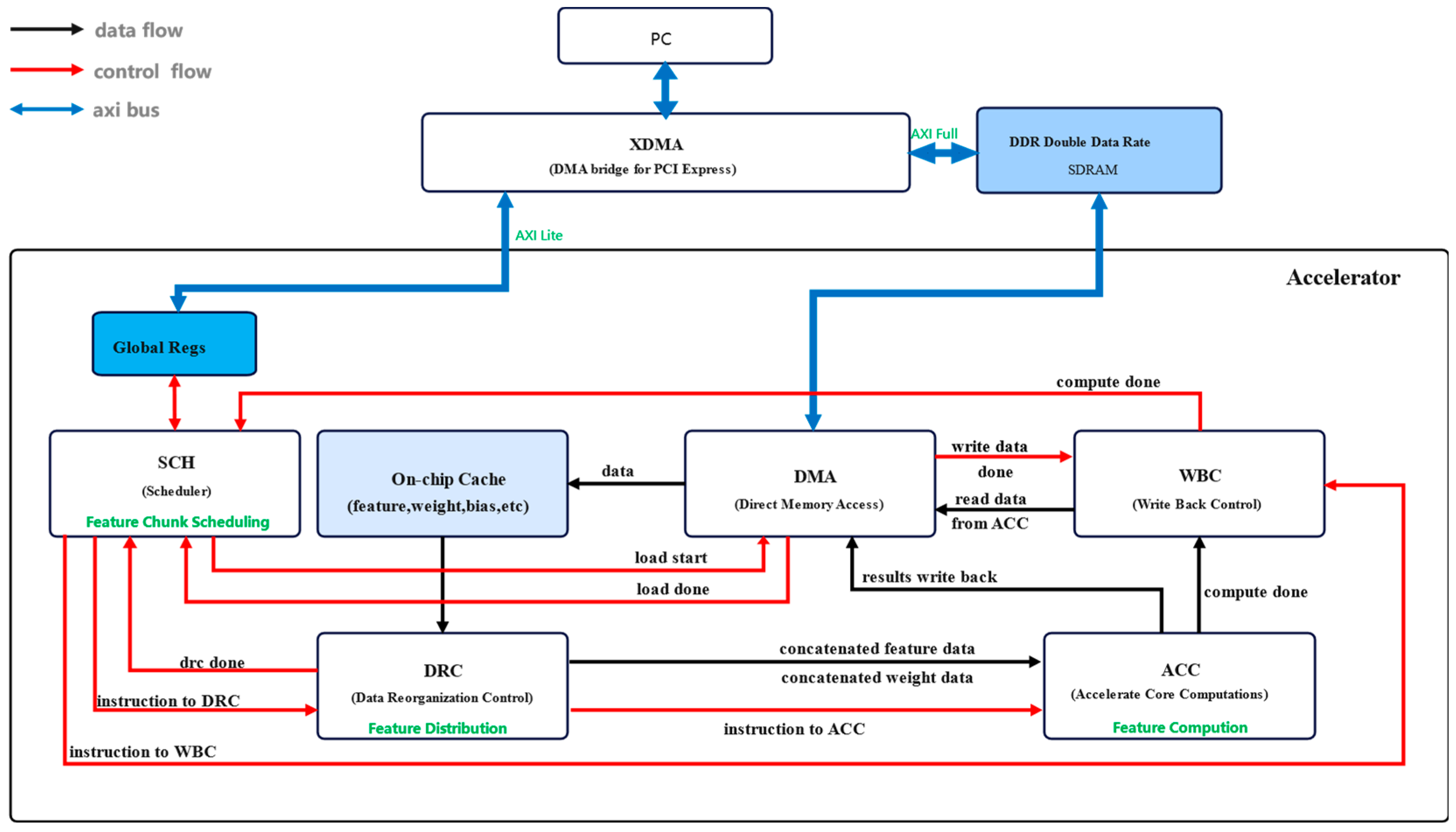
3.5. Proposed Hardware Architecture

The core idea of our proposed accelerator has been introduced in a previous context. Figure 26 illustrates the overall architecture of the proposed hardware accelerator for CNN. The AXI4 bus is responsible for data transfer, while the AXI_Lite bus manages instruction transfer. The key components of this CNN accelerator include the Scheduler (SCH) module, Direct Memory Access (DMA) module, Data Reorganization Control (DRC) module, Accelerate Core Computations (ACC) module, and Write-Back Control (WBC) module. The internal registers of the accelerator store detailed information about memory addresses and network layer parameters.
The DMA module handles data transfer requests between the accelerator and external memory interfaces. The Scheduler decomposes the computation of the entire network layer into block computation requests in the row and column directions, and controls the DMA to load input features. The DRC module guides the distribution of feature data, weight data, and instruction data to the ACC module.
The ACC is divided into a main computing unit and an auxiliary computing unit. When T N = 64 and T C = 8 , there are T N / T C computing groups, with each group consisting of T N / T C CVUs. These CVUs are connected through a Block Result RAM and jointly perform convolution, pooling, and activation operations, as shown in Figure 27. By controlling the accumulation mode, T N CVUs output feature maps of size T N × 8 or T N × 1 . By reusing weight data, each channel group computes T N × T R × T C output features, which are stored in the Block Result RAM. The final calculation result is obtained by switching channel groups and accumulating the outputs. The summed results in the Block Result RAM, of size T N × T R × T C , can be further processed through activation, pooling, and saturation truncation. Finally, the results are remapped to the WB RAM based on the feature layout address, and the WBC unit initiates block-wise computations by switching weights to achieve an output size of N × T R × T C .

4. Experiments

4.1. Experimental Design

This study focuses on the hardware acceleration of convolutional network layers with large images and small channels, as well as small images and large channels. The design utilizes a significant amount of RAM resources with low block address depth utilization. Therefore, the Xilinx’s Virtex UltraScale+ HBM VCU128 FPGA evaluation kit was chosen for experimentation. The board is equipped with 4GB DDR4 SDRAM and utilizes the Virtex7 series FPGA chip (model xcvu37p-fsvh2892), which provides sufficient resources for evaluating our design. We selected the Vivado 2020.02 IDE provided by Xilinx and used the Verilog hardware description language to write the code.
VGG-16 [30] is a classic model in deep neural networks, and has typical 3 × 3 convolution kernels, 1 step convolution operations, and a large fully connected layer. VGG-16 was chosen as the experimental object because it has been widely validated in previous studies and there is a large amount of comparative data available for reference. The complex structure and significant computation and data volume of VGG-16 enable it to comprehensively evaluate the performance of our developed CNN inference accelerator in processing computationally intensive tasks and large-scale data. In the experiment, the convolutional accelerator module was set to run at a clock frequency of 100 MHz, processing 8-bit quantized input feature maps and weights and verifying accuracy and efficiency by comparing the results of software calculations and hardware acceleration.
We can evaluate the efficiency of the computational array by tracking the effective number of working cycles of the multiply-accumulate array in the computing layer. The effective number of working cycles of the tracking multiplication and accumulational array in the computing layer starts from the start signal of the first block calculation and continues until the end signal of the last block calculation has been written back. We can calculate the efficiency of a multiply accumulate array by dividing its effective working cycles by the total number of cycles in the computing layer. The timing chart for computing unit performance statistics is shown in Figure 28, where total_cycles are recorded from sch_start signal to wb_done.
The total number of cycles are used for the ‘done’ signal, while valid_ cycles records the effective working time of the multiplier within this time range. By multiplying and accumulating the number of effective cycles of the array, we can gain a deeper understanding of the actual performance of the computational array throughout the entire calculation process, in order to better optimize and adjust the hardware design.
In order to measure the computational power of the accelerator, we chose OPS as an evaluation metric, which is expressed in Equation (5).
O P S = O P s T = R × C × N × M × K × K × 2 t o t a l _ c y c l e s × C l o c k   P e r i o d
where R × C denotes the size of the output feature map, N × M denotes the product of the number of output channels and the number of input channels, K denotes the size of the convolutional kernel, and T denotes the total time consumed by one layer of computation. Multiplication by 2 is due to the fact that OPS calculates the number of multiply–add operations per unit of time, which remains constant for each layer.
The utilization of the computation array (UCA) was measured and can be expressed in Equation (6).
U C A = T m u l t T = v a l i d _ c y c l e s × C l o c k   P e r i o d t o t a l _ c y c l e s × C l o c k   P e r i o d

4.2. Results and Discussions

Table 1 shows the performance of the three fully connected layers of VGG16. Since the data width is 64 bytes and there are 512 multipliers, the computation array can start computing every eight clock cycles. Therefore, the theoretical performance is 64/512 = 12.5%. Considering the time consumed by other logic, the actual performance of the fully connected layer is about 10.5%.
Table 2 shows the results for the height chunking size T R = 8 , Table 3 shows the results for the height chunking size T R = 16 , and Table 4 shows the results for the height chunking size T R = 32 .
From Table 2, it can be seen that the utilization rate of computing resources in each layer is above 99%, indicating that the accelerator is designed to be reasonably efficient. It solves the problem of the low utilization of computational arrays in traditional multi-channel parallel CNN hardware acceleration methods for large images with small channels.
Some UCA indicators for convolutional layers were slightly improved in Table 2, such as conv3 and conv4. This may be because the increase in T R values improves the degree of weight reuse, reducing the occurrence of UCA situations caused by weight loading, which has a positive impact. However, starting from conv5, there is a slight decrease in the computational performance of the network layers. This is likely due to the channel-first rearrangement of the output features, which results in a long period without feature data write-back. When the feature rearrangement has been completed, there will be a burst of continuous large-scale writes, which occupies the data bandwidth.
The conclusions drawn from Table 3 are similar to those from Table 2. With an increase in the T R value, there is a significant improvement in UCA in the conv2 layer. However, a decline in UCA is observed from the conv3 layer, indicating that with larger T R values, the generation of more output feature data intensifies the occupation of the data bandwidth, leading to a decline in performance.
In summary, from the three tables above, we can draw the following conclusions: for smaller output channels, employing a larger T R value can enhance the efficiency of UCA as it allows for more effective weight reuse. However, for larger output channels, a larger T R value may increase the back pressure of feature write-back, leading to negative effects. Additionally, since the pooling operation itself is a downsampling process aimed at reducing the number of output features, the fusion of convolution and pooling can alleviate the pressure of feature write-back, thereby maintaining a higher T R value.
Due to the shallow depth of RAM cache features and weight data used in each computation unit, we ended up using a large number of RAMs, but not all of them were fully utilized. The resources available on different FPGA platforms and whether or not the architecture design is specifically tailored for FPGA platforms can both impact the frequency of FPGA designs. Specifically, our goal is to study the contribution of computation units to throughput, so we aimed to minimize the impact of frequency differences on evaluation metrics in order to obtain a fairer comparison. Therefore, we used GOPS/DSP/freq (10−3) to emphasize the contribution of each DSP unit to the actual throughput. The results of comparing this design with other methods are shown in Table 5. In the table, this design implementation has a cell performance per 2.00 GOPS/DSP/freq (10−3), which exceeds other methods.

5. Conclusions

In this study, a method to design a high-throughput efficient CNN accelerator is presented. The proposed computational mapping method and feature-group-based data arrangement, through the implementation of a CNN hardware accelerator, achieved the design goal well and achieved high computation array utilization for both large graph and small channel and small graph and large channel cases. The proposed configurable vector unit supported vector aggregation accumulation and element-by-element accumulation, which improved the mapping efficiency of the network layer computation. The on-chip cache size was further optimized by using a feature block grouping data arrangement approach combined with a designed feature cache circuit and output feature remapping, which improved the input feature cache hit rate and reduced additional memory accesses. A performance statistics register was built into the hardware accelerator, and the direction of further performance optimization of the architecture was explored by investigating the impact of different T R parameters on the computation array utilization. Finally, with 512 DSPs running at 100 M mainframe frequency, the design in this paper achieved a maximum average computational capacity of 102.3 GOPS and a computation array utilization of 99.88%. Compared with other comparative methods, the design in this paper significantly improved the computation array utilization, achieved high throughput close to the theoretical limit, and had a higher computational density per unit multiplier.
This article does not discuss the situation in which the entire accelerator is packaged as a computing core, necessitating multiple computing cores to accelerate a layer of networks simultaneously. However, we believe that the proposed feature distribution method, combined with this input feature cache management method, can bring significant benefits to highly segmented and parallel accelerated output features. Therefore, compared to simply expanding the computing array, this method can further improve the computing peak under the stable efficiency of the computing array, which is not achievable by general methods. Furthermore, based on this feature cache design approach, it is also possible to make simple modifications to support larger convolutional kernels.

Author Contributions

Conceptualization, J.H., M.Z. and J.X.; methodology, J.H., M.Z., J.X., L.Y. and W.L.; software, J.H.; validation, J.H., M.Z., J.X. and L.Y.; formal analysis, J.H., M.Z., J.X., L.Y. and W.L.; investigation, J.H., M.Z., J.X., L.Y. and W.L.; writing—original draft preparation, J.H.; writing—review and editing, J.H., M.Z., J.X., L.Y. and W.L.; supervision, J.X., L.Y. and W.L.; project administration, J.X. and W.L. All authors have read and agreed to the published version of the manuscript.

Funding

This work was supported by the Key-Area Research and Development Program of Guangdong Province (Grant No. 2019B010107001).

Data Availability Statement

Publicly available datasets were analyzed in this study. The ImageNet dataset can be found here: https://www.image-net.org/ (accessed on 10 December 2023).

Conflicts of Interest

We declare that we have no financial and personal relationships with other people or organizations that can inappropriately influence our work, and there are no professional or other personal interests of any nature or kind in any product, service, and/or company that could be construed as influencing the position presented in, or the review of, the manuscript entitled.

References

  1. Krizhevsky, A.; Sutskever, I.; Hinton, G. ImageNet classification with deep convolutional neural networks. Commun. ACM 2017, 60, 84–90. [Google Scholar] [CrossRef]
  2. Girshick, R.; Donahue, J.; Darrell, T.; Malik, J. Rich feature hierarchies for accurate object detection and semantic segmentation tech report. In Proceedings of the IEEE 2014 IEEE Conference on Computer Vision and Pattern Recognition (CVPR), Columbus, OH, USA, 23–28 June 2014; pp. 580–587. [Google Scholar]
  3. Bontar, J.; Lecun, Y. Stereo matching by training a convolutional neural network to compare image patches. J. Mach. Learn. Res. 2016, 17, 1–32. [Google Scholar]
  4. Sandler, M.; Howard, A.; Zhu, M.; Zhmoginov, A.; Chen, L.-C. MobileNetV2: Inverted Residuals and Linear Bottlenecks. In Proceedings of the 2018 IEEE/CVF Conference on Computer Vision and Pattern Recognition (CVPR), Salt Lake City, UT, USA, 18–23 June 2018; IEEE: Piscataway, NJ, USA, 2018. [Google Scholar]
  5. Iandola, F.N.; Han, S.; Moskewicz, M.W.; Ashraf, K.; Dally, W.J.; Keutzer, K. Squeezenet: Alexnet-level accuracy with 50x fewer parameters and <0.5 mb model size. arXiv 2016, arXiv:1602.07360. [Google Scholar]
  6. Liang, S.; Yin, S.; Liu, L.; Luk, W.; Wei, S. FP-BNN: Binarized neural network on FPGA. Neurocomputing 2018, 275, 1072–1086. [Google Scholar] [CrossRef]
  7. Shen, Y.; Ferdman, M.; Milder, P. Overcoming resource underutilization in spatial CNN accelerators. In Proceedings of the 2016 26th International Conference on Field Programmable Logic and Applications (FPL), Lausanne, Switzerland, 29 August–2 September 2016; IEEE: Piscataway, NJ, USA, 2016; pp. 1–4. [Google Scholar]
  8. Liang, Y.; Lu, L.; Xiao, Q.; Yan, S. Evaluating fast algorithms for convolutional neural networks on FPGAs. IEEE Trans. Comput. Aided Des. Integr. Circuits Syst. 2019, 39, 857–870. [Google Scholar] [CrossRef]
  9. Ma, Y.; Cao, Y.; Vrudhula, S.; Seo, J.-S. An automatic RTL compiler for high-throughput FPGA implementation of diverse deep convolutional neural networks. In Proceedings of the 2017 27th International Conference on Field Programmable Logic and Applications (FPL), Ghent, Belgium, 4–8 September 2017; IEEE: Piscataway, NJ, USA, 2017; pp. 1–8. [Google Scholar]
  10. Ma, Y.; Cao, Y.; Vrudhula, S.; Seo, J.-S. Optimizing the Convolution Operation to Accelerate Deep Neural Networks on FPGA. IEEE Trans. Very Large Scale Integr. (VLSI) Syst. 2018, 26, 1354–1367. [Google Scholar] [CrossRef]
  11. Venieris, S.I.; Bouganis, C.S. Latency-driven design for FPGA-based convolutional neural networks. In Proceedings of the 2017 27th International Conference on Field Programmable Logic and Applications (FPL), Ghent, Belgium, 4–8 September 2017; IEEE: Piscataway, NJ, USA, 2017; pp. 1–8. [Google Scholar]
  12. Shen, Y.; Ferdman, M.; Milder, P. Maximizing CNN Accelerator Efficiency Through Resource Partitioning. ACM SIGARCH Comput. Arch. News 2017, 45, 535–547. [Google Scholar] [CrossRef]
  13. Zhang, C.; Sun, G.; Fang, Z.; Zhou, P.; Cong, J. Caffeine: Towards uniformed representation and acceleration for deep convolutional neural networks. In Proceedings of the ACM Turing Award Celebration Conference, Wuhan, China, 28–30 July 2023; pp. 47–48. [Google Scholar]
  14. Nguyen, D.T.; Nguyen, T.N.; Kim, H.; Lee, H.-J. A high-throughput and power-efficient FPGA implementation of YOLO CNN for object detection. IEEE Trans. Very Large Scale Integr. (VLSI) Syst. 2019, 27, 1861–1873. [Google Scholar] [CrossRef]
  15. Zhu, H.; Wang, Y.; Shi, C.-J.R. Tanji: A General-purpose Neural Network Accelerator with Unified Crossbar Architecture. IEEE Des. Test 2019, 37, 56–63. [Google Scholar] [CrossRef]
  16. Qiao, R.; Gang, C.; Gong, G.; Chen, G. High performance reconfigurable accelerator for deep convolutional neural networks. J. Xidian Univ. 2019, 3, 136–145. [Google Scholar]
  17. Shen, Y.; Ferdman, M.; Milder, P. Escher: A CNN Accelerator with Flexible Buffering to Minimize Off-Chip Transfer. In Proceedings of the 2017 IEEE 25th Annual International Symposium on Field-Programmable Custom Computing Machines (FCCM), Napa, CA, USA, 30 April–2 May 2017; IEEE: Piscataway, NJ, USA, 2017. [Google Scholar]
  18. Alawad, M.; Lin, M. Scalable FPGA accelerator for deep convolutional neural networks with stochastic streaming. IEEE Trans. Multi Scale Comput. Syst. 2018, 4, 888–899. [Google Scholar] [CrossRef]
  19. Xia, M.; Huang, Z.; Tian, L.; Wang, H.; Chang, V.; Zhu, Y.; Feng, S. Sparknoc: An energy-efficiency FPGA-based accelerator using optimized lightweight CNN for edge computing. J. Syst. Archit. 2021, 115, 101991. [Google Scholar] [CrossRef]
  20. Basalama, S.; Sohrabizadeh, A.; Wang, J.; Guo, L.; Cong, J. FlexCNN: An end-to-end framework for composing CNN accelerators on FPGA. ACM Trans. Reconfigurable Technol. Syst. 2023, 2, 16. [Google Scholar] [CrossRef]
  21. Huang, W.; Wu, H.; Chen, Q.; Luo, C.; Zeng, S.; Li, T.; Huang, Y. FPGA-Based High-Throughput CNN Hardware Accelerator with High Computing Resource Utilization Ratio. IEEE Trans. Neural Netw. Learn. Syst. 2021, 33, 4069–4083. [Google Scholar] [CrossRef] [PubMed]
  22. Li, H.; Fan, X.; Jiao, L.; Cao, W.; Zhou, X.; Wang, L. A high performance FPGA-based accelerator for large-scale convolutional neural networks. In Proceedings of the 2016 26th International Conference on Field Programmable Logic and Applications (FPL), Lausanne, Switzerland, 29 August–2 September 2016; IEEE: Piscataway, NJ, USA, 2016; pp. 1–9. [Google Scholar]
  23. Shan, J.; Lazarescu, M.T.; Cortadella, J.; Lavagno, L.; Casu, M.R. CNN-on-AWS: Efficient Allocation of Multikernel Applications on Multi-FPGA Platforms. IEEE Trans. Comput. Des. Integr. Circuits Syst. 2020, 40, 301–314. [Google Scholar] [CrossRef]
  24. Yin, S.; Tang, S.; Lin, X.; Ouyang, P.; Tu, F.; Liu, L.; Wei, S. A High Throughput Acceleration for Hybrid Neural Networks with Efficient Resource Management on FPGA. IEEE Trans. Comput. Des. Integr. Circuits Syst. 2018, 38, 678–691. [Google Scholar] [CrossRef]
  25. Sze, V.; Chen, Y.-H.; Yang, T.-J.; Emer, J. Efficient processing of deep neural networks: A tutorial survey. Proc. IEEE 2017, 105, 2295–2329. [Google Scholar] [CrossRef]
  26. Liu, Z.; Dou, Y.; Jiang, J.; Wang, Q.; Chow, P. An FPGA-based processor for training convolutional neural networks. In Proceedings of the 2017 International Conference on Field Programmable Technology (ICFPT), Melbourne, Australia, 11–13 December 2017; IEEE: Piscataway, NJ, USA, 2017. [Google Scholar]
  27. Chen, T.; Du, Z.; Sun, N.; Wang, J.; Wu, C.; Chen, Y. DianNao: A small-footprint high-throughput accelerator for ubiquitous machine-learning. ACM SIGPLAN Not. 2014, 49, 269–284. [Google Scholar] [CrossRef]
  28. Liu, J.; Zhang, C. A Multi-Scale Neural Network for Traffic Sign Detection Based on Pyramid Feature Maps. In Proceedings of the 2019 IEEE 21st International Conference on High Performance Computing and Communications, Zhangjiajie, China, 10–12 August 2019; IEEE: Piscataway, NJ, USA, 2019. [Google Scholar]
  29. Putra, R.V.W.; Hanif, M.A.; Shafique, M. ROMANet: Fine-Grained Reuse-Driven Off-Chip Memory Access Management and Data Organization for Deep Neural Network Accelerators. IEEE Trans. Very Large Scale Integr. (VLSI) Syst. 2021, 29, 702–715. [Google Scholar] [CrossRef]
  30. Simonyan, K.; Zisserman, A. Very deep convolutional networks for large-scale image recognition. arXiv 2014, arXiv:1409.1556. [Google Scholar]
  31. Jia, H.; Ren, D.; Zou, X. An FPGA-based accelerator for deep neural network with novel reconfigurable architecture. IEICE Electron. Express 2021, 18, 20210012. [Google Scholar] [CrossRef]
  32. Zeng, S.; Huang, Y. A Hybrid-Pipelined Architecture for FPGA-based Binary Weight DenseNet with High Performance-Efficiency. In Proceedings of the 2020 IEEE High Performance Extreme Computing Conference (HPEC), Waltham, MA, USA, 22–24 September 2020. [Google Scholar]
  33. Yu, Y.; Wu, C.; Zhao, T.; Wang, K.; He, L. OPU: An FPGA-Based Overlay Processor for Convolutional Neural Networks. IEEE Trans. Very Large Scale Integr. (VLSI) Syst. 2020, 28, 35–47. [Google Scholar] [CrossRef]
Figure 1. Mapping diagram of channel group parallel computation.
Electronics 13 01050 g001
Figure 2. Schematic diagram of channel group parallel computation mapping based on feature group data layout.
Electronics 13 01050 g002
Figure 3. Comparison of computation array working modes: (a) parallelism with multiple output features vs. (b) parallelism with single output feature.
Electronics 13 01050 g003
Figure 4. Address mapping for G C · R T C M data format.
Electronics 13 01050 g004
Figure 5. Address mapping for RMC data format.
Electronics 13 01050 g005
Figure 6. K = 3 , S = 1 schematic of feature chunk loading. (a) Diagram illustrating the loading of Cube1 and Cube2. (b) Diagram illustrating the loading of Cube3.
Electronics 13 01050 g006
Figure 7. K = 3 , S = 2 schematic of feature chunk loading. (a) Diagram illustrating the loading of Cube1 and Cube2. (b) Diagram illustrating the loading of Cube3 and Cube4.
Electronics 13 01050 g007
Figure 8. Schematic diagram of the feature cache array.
Electronics 13 01050 g008
Figure 9. Schematic diagram of on-chip address mapping for RMC format features.
Electronics 13 01050 g009
Figure 10. Schematic diagram of on-chip address mapping for G C · R T C M format features.
Electronics 13 01050 g010
Figure 11. Schematic of output feature map chunking calculation with input feature sizes.
Electronics 13 01050 g011
Figure 12. RMC format feature computation mode: K = 3 , S = 1 / 2 as an example.
Electronics 13 01050 g012
Figure 13. Control logic under RMC format: K = 3 , S = 1 / 2 as an example.
Electronics 13 01050 g013
Figure 14. Diagram of feature stitching and scheduling for sub-chunk computation based on RMC format features.
Electronics 13 01050 g014
Figure 15. Diagram of K = 3 , S = 2 feature selection in RMC format.
Electronics 13 01050 g015
Figure 16. Diagram of K = 3 , S = 2 feature splicing in RMC format.
Electronics 13 01050 g016
Figure 17. Diagram of K = 3 , S = 1 feature selection in RMC format.
Electronics 13 01050 g017
Figure 18. Diagram of K = 3 , S = 1 feature splicing in RMC format.
Electronics 13 01050 g018
Figure 19. G C · R T C M format feature computation mode: K = 3 , S = 1 as an example.
Electronics 13 01050 g019
Figure 20. Control logic under G C · R T C M format: K = 3, S = 1 as an example.
Electronics 13 01050 g020
Figure 21. Feature splicing and scheduling diagram for sub-chunk computation based on G C · R T C M format features: K = 3, S = 1 as an example.
Electronics 13 01050 g021
Figure 22. Diagram of feature splicing in G C · R T C M format.
Electronics 13 01050 g022
Figure 23. Design of feature distribution circuit.
Electronics 13 01050 g023
Figure 24. Detailed design of multiply-accumulate logic for CVU.
Electronics 13 01050 g024
Figure 25. Diagram of weight transformation (a) in G C · R T C M format vs. (b) in R M C format.
Electronics 13 01050 g025
Figure 26. The overall architecture of the proposed hardware accelerator.
Electronics 13 01050 g026
Figure 27. Overall structure of the ACC module.
Electronics 13 01050 g027
Figure 28. The timing diagram for performance statistics of the computation array.
Electronics 13 01050 g028
Table 1. UCA in each fully connected layer of VGG16.
LayerTotal CyclesValid CyclesUCA
fc1262,1442,461,44610.65
fc232,768309,13210.60
fc3819277,94410.51
Table 2. UCA in each calculation layer of VGG16 when T R = 8 .
LayerShapeTotal CyclesValid CyclesUCA
conv1(3, 64, 3, 1)222,251221,18499.52
conv2(64, 64, 3, 1)4,726,2154,718,59299.84
conv2-pool(64, 64, 3, 1)4,726,2274,718,59299.84
conv3(64, 128, 3, 1)2,361,6152,359,29699.90
conv4(128, 128, 3, 1)4,721,0614,718,59299.95
conv4-pool(128, 128, 3, 1)4,720,9864,718,59299.95
conv5(128, 256, 3, 1)2,360,5492,359,29699.95
conv6(256, 256, 3, 1)4,720,1494,718,59299.97
conv7(256, 256, 3, 1)4,720,1494,718,59299.97
conv7-pool(256, 256, 3, 1)4,719,9944,718,59299.97
conv8(512, 512, 3, 1)2,360,7782,359,29699.94
conv9(512, 512, 3, 1)4,720,7084,718,59299.96
conv10(512, 512, 3, 1)4,720,6814,718,59299.96
conv10-pool(512, 512, 3, 1)4,719,7544,718,59299.98
conv11(512, 512, 3, 1)1,181,5891,179,64899.84
conv12(512, 512, 3, 1)1,181,6241,179,64899.83
conv13(512, 512, 3, 1)1,181,5871,179,64899.84
conv13-pool(512, 512, 3, 1)1,180,7261,179,64899.91
Table 3. UCA in each calculation layer of VGG16 when T R = 16 .
LayerShapeTotal CyclesValid CyclesUCA
conv1(3, 64, 3, 1)222,251221,18499.52
conv2(64, 64, 3, 1)4,722,8884,718,59299.91
conv2-pool(64, 64, 3, 1)4,722,8264,718,59299.91
conv3(64, 128, 3, 1)2,361,0372,359,29699.93
conv4(128, 128, 3, 1)4,720,6114,718,59299.96
conv4-pool(128, 128, 3, 1)4,720,4744,718,59299.96
conv5(128, 256, 3, 1)2,360,9052,359,29699.93
conv6(256, 256, 3, 1)4,720,7954,718,59299.95
conv7(256, 256, 3, 1)4,720,7954,718,59299.95
conv7-pool(256, 256, 3, 1)4,720,4724,718,59299.96
conv8(512, 512, 3, 1)2,361,7862,359,29699.89
conv9(512, 512, 3, 1)4,721,0524,718,59299.95
conv10(512, 512, 3, 1)4,722,1724,718,59299.92
conv10-pool(512, 512, 3, 1)4,720,5344,718,59299.96
conv11(512, 512, 3, 1)1,182,0041,179,64899.80
conv12(512, 512, 3, 1)1,182,0041,179,64899.80
conv13(512, 512, 3, 1)1,182,0401,179,64899.80
conv13-pool(512, 512, 3, 1)1,181,4841,179,64899.84
Table 4. UCA in each calculation layer of VGG16 when T R = 32 .
LayerShapeTotal CyclesValid CyclesUCA
conv1(3, 64, 3, 1)222,250221,18499.52
conv2(64, 64, 3, 1)4,721,6334,718,59299.94
conv2-pool(64, 64, 3, 1)4,721,4814,718,59299.94
conv3(64, 128, 3, 1)2,361,2352,359,29699.92
conv4(128, 128, 3, 1)4,721,0634,718,59299.95
conv4-pool(128, 128, 3, 1)4,720,7944,718,59299.95
conv5(128, 256, 3, 1)2,361,3802,359,29699.91
conv6(256, 256, 3, 1)4,722,3074,718,59299.92
conv7(256, 256, 3, 1)4,722,2924,718,59299.92
conv7-pool(256, 256, 3, 1)4,721,8034,718,59299.93
conv8(512, 512, 3, 1)2,362,8342,359,29699.85
conv9(512, 512, 3, 1)4,723,1544,718,59299.90
conv10(512, 512, 3, 1)4,723,1524,718,59299.90
conv10-pool(512, 512, 3, 1)4,724,2284,718,59299.88
conv11(512, 512, 3, 1)---
conv12(512, 512, 3, 1)---
conv13(512, 512, 3, 1)---
conv13-pool(512, 512, 3, 1)---
Table 5. Comparison of performance on VGG-16.
[31][15][32][33]Our
PlatformFPGAFPGAFPGAFPGAFPGA
Clock (MHz)140165200200100
Precision (bit)1616888
#RAMNA249.51765193.5773.5
DSP5762562877704512
Throughput(GOPS)129.766.931805.83176102.27
GOPS/DSP/freq(10−3)1.601.581.331.252.00
Disclaimer/Publisher’s Note: The statements, opinions and data contained in all publications are solely those of the individual author(s) and contributor(s) and not of MDPI and/or the editor(s). MDPI and/or the editor(s) disclaim responsibility for any injury to people or property resulting from any ideas, methods, instructions or products referred to in the content.

