Abstract
In this paper, a filtered differential phase shifter with good selectivity is proposed and constructed. This study proposes and builds a filtered differential phase shifter with good selectivity. The main and reference lines in the suggested filtered differential phase shifter are structurally identical. The main line’s bandpass filtering function is achieved by a new coupled feeder, a parallel coupled line loaded with shorted branches, and a coupled resonator at the load end. It has impedance matching and additional transmission zeros/poles. By loading the coupled resonator at the load end, the selectivity of the phase shifter can be improved and the passband and transmission zeros/poles of the phase shifter can be equitably distributed by varying the coupling coefficients and the electrical lengths of the loaded branches. The reference line is a coupled resonator with the same structure and its electrical length is related to the number of degrees of phase shift. Finally, a differential phase shifter is designed and measured. The fractional bandwidth of the proposed phase shifter is about 38%, the return loss reaches −11 dB, the insertion loss is about 1.02 dB, the deviation of the simulated results in terms of the number of degrees of phase shift is about 2.5 degrees, and the deviation of the tested results is about 6 degrees. The trend of the simulation results and the actual measurement results are in good agreement.
1. Introduction
Phase shifter is the electronic device or circuit used to change the phase of a signal. It plays an important role in electronic and communication systems, and is widely used in polarization redistribution antennas, electronically scanned radars, broadband branch-line baluns, wireless communications, circularly polarized reflector arrays, and other systems. In the common phase modulation communication system, the phase shifter can adjust the phase of the signal. By adjusting the phase shifter, the pAAArecise control of the phase of the signal can be realized, and the transmission of information can be realized, which effectively improves the performance and efficiency of the communication system. In phased array radar and satellite communication systems, phase shifters are used in beamforming [1] for adjusting the phase of each element in the antenna array. By changing the phase of the signal, the phase relationship of each unit in the antenna array can be controlled to achieve the direction adjustment of the beam for electronic scanning and beamforming. In communication systems, phase shifters [2] do not require any additional new analog hardware to be fabricated. One-bit phase shifters are used for full-duplex millimeter-wave communication and can be used to adjust the phase of the signal. Ref. [3] fabricated 27–42 GHz 5-bit passive switching phase shifters for the signal synthesis, and the separation, being used in 5G applications. The phase shifter can be used to adjust the phase of the received signal in an interference environment to minimize the effect of interference on the signal [4]. Tunable phase shifters are designed using tunable capacitors as reflective loads. Phase shifters provide a flexible way to adjust the phase without changing the hardware architecture, which makes the system design more flexible and reconfigurable. A phase shifter with a 90° or 180° phase difference serves as a key circuit element. A lot of research has been carried out by researchers to design different types of phase shifters [5,6,7,8,9,10].
Conventional phase shifters change the phase by varying the length of the transmission line or the propagation constant, but this usually results in a narrow bandwidth. In 1958, Schiffman designed a 90° differential phase shifter using an edge-coupled stripline structure [5]. Since then, various improvements have been made to the Schiffman phase shifter to obtain wider-bandwidth phase shifts, such as the use of different types of coupled-line structures [11], which have a tunable differential phase shifter with broadband phase characteristics and a maximum in-band phase error of ±8.6° [12]. Fabricating a phase shifter with a larger bandwidth using a multilayer structure employing a semi-elliptic edge-coupled structure would make the structure more complex and the fabricated circuit larger. The selection of superconductor materials [4] for superconducting phase shifters with adjustable phase shifts for full microwave transmission suitable for quantum computing and technology can effectively reduce the size of the device, but it is also expensive in terms of fabrication. Configurations proposed in the literature [13] have a 90° phase shifter function that utilizes lateral coupling between two microstrip patches, realized through slots located in a common ground plane. These phase shifter designs have a large phase imbalance, which is a limitation for applications requiring highly accurate phase control. On the other hand, some differential phase shifter designs may suffer from narrow bandwidth. A class of planar miniature arbitrary phase difference couplers [14,15] with arbitrary coupling coefficients can provide arbitrary coupling coefficients and arbitrary phase differences, but their phase shift bandwidth is only 20% and they have no filtering. The large phase shift deviation at the band edge limits their use in broadband applications. Ref. [16] provides a design method for arbitrary phase difference, but it also has a narrow bandwidth and poor out-of-band performance.
Recently, the selectivity of bandpass filters and phase-shifter-integrated devices [17,18] has attracted extensive interest from researchers. Poor passband selectivity leads to insufficient out-of-band signal rejection, which may cause inter-signal interference, especially in dense-frequency usage environments. T-type open branch-loaded transmission line structures [6], and coplanar waveguide mouse couplers [19], are complex, and the reference line of the phase shifter has to be modified each time to meet the requirements for different output phase differences. The increase in the circuit network in turn leads to an increase in the return loss and size of the circuit, resulting in a decrease in circuit performance. Inconvenient calculation methods are difficult to apply in practice, which greatly limits the generality of the device. To compensate for poor passband selectivity, additional circuit components may be required, which can increase circuit complexity and cost, for example, cascading multiple resonators to increase the order of the filter, utilizing a multilayer PCB structure, or using superconducting materials. However, for the fabrication of differential phase shifters, increasing the number of resonator orders will inevitably lead to redundant circuit structures and increase the size of the fabricated device; utilizing a multilayer structure will make the structure more complex; and selecting superconducting materials can effectively reduce the size of the device, but the cost of fabrication is also very expensive.
Therefore, in this paper, a highly selective differential phase shifter using a single-layer structure is proposed and the design methodology is analyzed in detail. The phase shifter considers both passband and loaded resonators, which are chosen to introduce additional transmission poles and zeros to improve the passband selectivity. The reference line section allows for phase shift values of 90 degrees. This section is a connected resonator structure similar to the main line. In addition, the measured results of the designed and fabricated phase shifter are in agreement with the simulated results.
2. Proposed Phase Shifter Structure
The structure of the suggested differential filter phase shifter is depicted in Figure 1. It can be separated into two parts: the reference line structure, which is green, and the primary line structure, which is red. The main line of the proposed differential phase shifter consists of a new coupled feed line set equipped with coupled resonators. The reference line has the same structure and its physical structure is identical to the main line. Both the main line and the reference line are symmetrical structures. The main line is cascaded by parallel coupled lines and branch-loaded short-circuited branches. For the main line, the new coupled feeder is cascaded by parallel coupled lines and short-circuited branches of certain electrical lengths (, ). By controlling the electrical length of the short-circuited branches, the coupled line can be made to exhibit short circuit characteristics at frequency . They have the same passband response at the center frequency when the frequency . The pole at the center frequency is generated by a one-half wavelength coupled line. Load-coupled resonators (, , ) are utilized to improve the passband rectangularity and bandwidth. In addition, the differential phase shifter in this paper has two main characteristics, i.e., phase difference and amplitude agreement. The phase is determined by the difference between the phases of the main and reference lines. The main and reference lines of the phase shifter are two-port networks. According to the microwave network theory, the insertion phase shift of the main and reference lines of the phase shifter can be expressed as
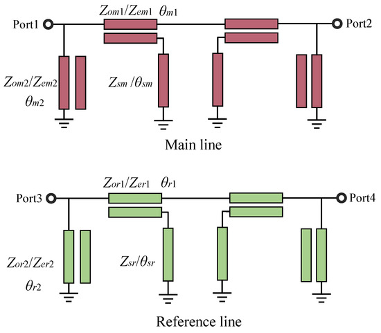
Figure 1.
Structure of the differential phase shifter.
3. Analysis and Design
Figure 2 depicts the generalized topology of a filtered differential phase shifter with high selectivity. It can be seen in Figure 2 that the phase shifter structure proposed in this paper is realized by a cascade network of generic topologies. For a conventional type path, the transmission matrix, i.e., the ABCD matrix, is
where and are the electrical lengths of the reference and main lines. For more generalization, both conventional paths are represented by transmission lines with equivalent characteristic impedance and electrical lengths , , where , are functions of , and their relationship is , with being the center frequency of the operating passband. Two identical networks with characteristic impedance and electrical length are connected in series before and after the two paths of the conventional network, where is also a function of . The main and reference lines’ amplitude and phase response are computed as
where is the phase characteristic, represents the transmission coefficient, i = m corresponds to the main line of the phase shifter, and i = r denotes the reference line of the phase shifter. From Equation (1), the phase is determined by the difference between the phases of the main and reference lines. The phase difference is determined by the design parameters of the circuit, while the amplitude uniformity ensures that the two output signals have the same strength to maintain the quality and stability of the signals. Therefore, they can also be simplified by the above equation as
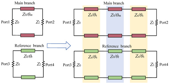
Figure 2.
Generalized topology of filtered differential phase shifter with high selectivity.
Figure 3 shows a schematic diagram of the topology corresponding to the circuit structure of a filtered phase shifter with high selectivity. It can be seen that the dark-green part is the circuit structure, while the main line corresponds to the circuit structure of the reference line. The lower part shows the topology of the whole phase shifter. The main and reference lines of the entire phase shifter are composed of a two-port network. Due to the cascaded two-port network, the ABCD matrix of the N cascaded ports is equal to the multiplication of the ABCD matrices of the individual ports. Therefore, starting from the conventional topology type depicted in Figure 2, the main and reference paths of the system in this paper are obtained through the cascaded network, and since the main and reference lines have the same structure, their transmission matrices, the ABCD matrices, can be obtained from the conventional topology shown in Figure 2 above, i.e., from Equation (2).
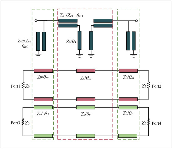
Figure 3.
Circuit model and topology of the filtered differential phase shifter with high selectivity.
The phase shift of the proposed phase shifter has been given by Equation (5), so, from the transmission matrix of this phase shifter, the amplitude equation can be derived as
4. Fabrication and Measurements
To verify the aforementioned concepts, a highly selective phase shifter with a center frequency of 3.6 GHz was designed and built following theoretical study. It achieves a phase shift of 90° ± 2.5° in the passband. The bandwidth is about 38.5%. A single-layer microstrip topology is used in this study. The substrate used is Rogers R5880 with a relative dielectric constant of 2.2 and a thickness of 0.78 mm. A Keysight N5224B was used as the measurement tool after additional analysis and adjustments using Advanced Design System2019. The final physical layout of the phase shifter suggested in this study is depicted in Figure 4. It is based on the circuit structure shown in Figure 1, where the physical dimensions of the loaded branches and each set of connected microstrip lines are determined using particular impedance values. It can be seen from the figure that it is a symmetrical structure consisting of three parts in cascade; the left and right parts are parity mode impedances with coupling, and the lowermost blue part is a grounded through-hole with a diameter of 2.5 mm. Table 1 shows the final configuration of the phase shifter, which was obtained by converting the theoretical parameters to physical dimensions and changing them slightly according to the theoretical variations.
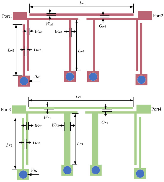
Figure 4.
Phase shifter layout.

Table 1.
Parameters of the proposed differential phase shifter.
Figure 5 and Figure 6 show the amplitude response and phase response of the phase shifter proposed in this paper. As can be seen from Figure 5, the simulation results show that the highly selective phase shifter has a 3 dB bandwidth of 38.5% in the frequency range of 2.70–4.71 GHz, with a minimum return loss better than 14.02 dB and an insertion loss of less than 0.51 dB. The load-shorting stubs introduce two transmission zeros near the passband cutoff edges at 2.98 and 4.48 GHz. Based on the measurements, the out-of-band rejection is about 30 dB in the frequency range from 4.3 GHz to 6.0 GHz, and the analog phase shift of the phase shifter is 90° ± 2.5° in the frequency range from 3.2 to 4.05 GHz, as shown in Figure 6. In the passband, the phase deviation of the differential phase shifter is about 6 degrees in the 3.1–4.1 Ghz range. The measurements further demonstrate the validity of the proposed design scheme as they are in general agreement with the layout simulation results.
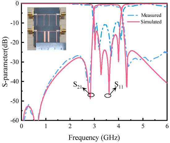
Figure 5.
Simulated and measured results of the designed 90° phase shifter.
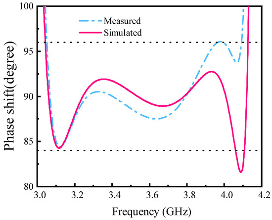
Figure 6.
Simulated and measured phase shift of the designed 90° phase shifter.
The trends of the measured and simulated data show a fair degree of consistency. The differential phase shifter has a fraction of roughly 38.5%, with an insertion loss less than −1.02 dB and return loss less than −11 dB. The phase shift of the differential phase shifter is measured to be 90° ± 6° over this frequency range. In the simulation, the phase shift introduced by the SMA connectors is not taken into account, and the SMA interfaces and solder joints introduce additional phase deviations that can lead to deviations between simulated and measured results. In physical machining experiments, the phase characteristics of differential phase shifters with different coupling spacing are also affected by machining errors (maximum machining error ±1 mil). These errors may lead to a slight deviation of the measured results from the simulated results. We have prepared Table 2 to further show the ratio between the designed phase shifter and other different phase shifters examined.
Table 2.
Comparison between the designed phase shifter and different configurations of other works.
5. Conclusions
In this paper, a filtered differential phase shifter with high selectivity is designed and fabricated, its implementation using cascade networks is methodically described, and its simulation principles and physical test functions are investigated and verified. To enhance the selectivity of the phase shifter, the in-band and out-of-band transmission poles and zeros are increased by using a novel coupled feeder with a load-coupled line resonator, and then the phase shift is further adjusted. This differential phase shifter structure can be made smaller, making it a more compact design than the conventional phase shifter structure that adds a microstrip line as a reference line. The layout and schematic simulation results correlate well with the measurements.
Author Contributions
Conceptualization, X.F., T.L., L.F., Y.M., W.X. and T.Z.; methodology, X.F., T.L., L.F. and W.X.; software, X.F., T.L., L.F., Y.M. and W.X.; formal analysis, X.F., T.L., L.F., Y.M. and W.X.; investigation, X.F., T.L., L.F., Y.M. and W.X.; resources, X.F., T.L. and L.F.; data curation, X.F., T.L., L.F., Y.M., W.X. and T.Z.; writing—original draft preparation, X.F., T.L., L.F., Y.M., W.X. and T.Z.; writing—review and editing, X.F., T.L., L.F., Y.M., W.X. and T.Z. All authors have read and agreed to the published version of the manuscript.
Funding
This work is the result of the research project funded by the Guangxi science and technology major special project (Gui Ke AA22068064) on remote intelligent remote control construction machinery research and application and Liuzhou science and technology program project (2022AAB0101) on remote intelligent remote control construction machinery research and application.
Data Availability Statement
The original contributions presented in the study are included in the article, and further inquiries can be directed to the corresponding author.
Conflicts of Interest
The authors declare that there is no conflict of interest. The supporting parties were not involved in the study design, data collection, analysis and interpretation, report writing and the decision whether to submit the report for publication. All authors have read and agreed to the submission of the published version of the manuscript to the journal.
References
- Szortyka, V.; Raczkowski, K.; Kuijk, M.; Wambacq, P. A wideband beamforming lowpass filter for 60 GHz phased-array receivers. IEEE Trans. Circuits Syst. Regul. Pap. 2015, 62, 2324–2333. [Google Scholar] [CrossRef]
- da Silva, J.M.B.; Sabharwal, A.; Fodor, G.; Fischione, C. 1-bit phase shifters for large-antenna full-duplex mmWave communications. IEEE Trans. Wirel. Commun. 2020, 19, 6916–6931. [Google Scholar] [CrossRef]
- Tsai, J.H.; Tung, Y.L.; Lin, Y.H. A 27–42-GHz low phase error 5-bit passive phase shifter in 65-nm CMOS technology. IEEE Microw. Wirel. Components Lett. 2020, 30, 900–903. [Google Scholar] [CrossRef]
- Liu, W.J.; Zheng, S.Y.; Pan, Y.M.; Li, Y.X.; Long, Y.L. A wideband tunable reflection-type phase shifter with wide relative phase shift. IEEE Trans. Circuits Syst. II Express Briefs 2017, 64, 1442–1446. [Google Scholar] [CrossRef]
- Schiffman, B. A new class of broad-band microwave 90-degree phase shifters. IRE Trans. Microw. Theory Tech. 1958, 6, 232–237. [Google Scholar] [CrossRef]
- Zheng, S.Y.; Chan, W.S.; Man, K.F. Broadband phase shifter using loaded transmission line. IEEE Microw. Wirel. Components Lett. 2010, 20, 498–500. [Google Scholar] [CrossRef]
- Wong, Y.S.; Zheng, S.Y.; Chan, W.S. Multi-way and poly-phase aligned feed-forward differential phase shifters. IEEE Trans. Microw. Theory Tech. 2014, 62, 1312–1321. [Google Scholar] [CrossRef]
- Lyu, Y.P.; Zhu, L.; Cheng, C.H. Dual-band differential phase shifter using phase-slope alignment on coupled resonators. IEEE Microw. Wirel. Components Lett. 2018, 28, 1092–1094. [Google Scholar] [CrossRef]
- Zhu, H.; Guo, Y.J. Wideband filtering phase shifter using transversal signal-interference techniques. IEEE Microw. Wirel. Components Lett. 2019, 29, 252–254. [Google Scholar] [CrossRef]
- Akbar, F.; Mortazawi, A. An integrated compact phase shifter with a single analog control. IEEE Microw. Wirel. Components Lett. 2021, 32, 410–413. [Google Scholar] [CrossRef]
- Wu, Y.; Shen, J.Y.; Liu, Y.; Leung, S.W.; Xue, Q. Miniaturized arbitrary phase-difference couplers for arbitrary coupling coefficients. IEEE Trans. Microw. Theory Tech. 2013, 61, 2317–2324. [Google Scholar] [CrossRef]
- Lo, Y.C.; Chung, B.K.; Lim, E.H. Design of wideband phase shifter with edge-coupled semi-elliptical lines. Microelectron. J. 2021, 114, 105143. [Google Scholar] [CrossRef]
- Zheng, S.Y.; Deng, J.H.; Pan, Y.M.; Chan, W.S. Circular sector patch hybrid coupler with an arbitrary coupling coefficient and phase difference. IEEE Trans. Microw. Theory Tech. 2013, 61, 1781–1792. [Google Scholar] [CrossRef]
- Zhu, H.; Abbosh, A.M. A compact tunable directional coupler with continuously tuned differential phase. IEEE Microw. Wirel. Components Lett. 2017, 28, 19–21. [Google Scholar] [CrossRef]
- Chaudhary, G.; Jeong, Y. Wideband tunable differential phase shifter with minimized in-band phase deviation error. IEEE Microw. Wirel. Components Lett. 2019, 29, 468–470. [Google Scholar] [CrossRef]
- Wong, Y.S.; Zheng, S.Y.; Chan, W.S. Quasi-arbitrary phase-difference hybrid coupler. IEEE Trans. Microw. Theory Tech. 2012, 60, 1530–1539. [Google Scholar] [CrossRef]
- Lyu, Y.P.; Zhu, L.; Cheng, C.H. Proposal and synthesis design of wideband filtering differential phase shifters with a pair of out-of-band transmission zeroes. IEEE Trans. Microw. Theory Tech. 2018, 66, 2828–2841. [Google Scholar] [CrossRef]
- Yu, X.; Chen, J.; Feng, L.; Zhu, L.; Liu, H. Synthesis design of wideband phase shifters using coupled-line structure. IEEE Microw. Wirel. Components Lett. 2022, 32, 515–518. [Google Scholar] [CrossRef]
- Yao, J.J.; Yeo, S.P. Six-port reflectometer based on modified hybrid couplers. IEEE Trans. Microw. Theory Tech. 2008, 56, 493–498. [Google Scholar]
- Guo, L.; Zhu, H.; Abbosh, A. Wideband phase shifter with wide phase range using parallel coupled lines and L-shaped networks. IEEE Microw. Wirel. Components Lett. 2016, 26, 592–594. [Google Scholar] [CrossRef]
- Singh, A.; Mandal, M.K. Electronically tunable reflection type phase shifters. IEEE Trans. Circuits Syst. II Express Briefs 2019, 67, 425–429. [Google Scholar] [CrossRef]
Disclaimer/Publisher’s Note: The statements, opinions and data contained in all publications are solely those of the individual author(s) and contributor(s) and not of MDPI and/or the editor(s). MDPI and/or the editor(s) disclaim responsibility for any injury to people or property resulting from any ideas, methods, instructions or products referred to in the content. |
© 2024 by the authors. Licensee MDPI, Basel, Switzerland. This article is an open access article distributed under the terms and conditions of the Creative Commons Attribution (CC BY) license (https://creativecommons.org/licenses/by/4.0/).