Article

Constructing a Microstrip Phase Shifter with Low Phase Error Using a Y-Resonator

1
School of Automation, Guangxi University of Science and Technology, Liuzhou 545000, China
2
College of Integrated Circuits and Optoelectronic Chips, Shenzhen Technology University, Shenzhen 518118, China
*
Author to whom correspondence should be addressed.
Electronics 2024, 13(24), 5006; https://doi.org/10.3390/electronics13245006
Submission received: 24 September 2024 / Revised: 15 November 2024 / Accepted: 18 December 2024 / Published: 19 December 2024

Abstract

:
In this paper, we propose a Y-type dual-mode microstrip phase shifter that utilizes input–output cross-coupling. The structure comprises a main line and a reference line, with the main line designed in a cross-coupled parallel-feeding configuration to create a band-pass filter. The single-mode resonance frequency is fine-tuned to meet the bandwidth requirements of the band-pass filter. Additionally, by introducing new symmetric transmission zeros in the upper and lower cutoff bands through the cross-coupling of the input and output feed lines, we achieve a quasi-elliptic response. This design significantly enhances both the passband and out-of-band performance of the filter. The reference line functions as a uniform transmission line, and the phase shift value of the phase shifter is achieved by adjusting its electrical length. Compared to conventional phase shifters, this design offers several advantages, including a simpler structure, reduced phase error, and a wider phase shift range. Ultimately, a 90° to 225° phase shifter was designed and simulated, while a 90° phase shifter was fabricated and tested. Measurement results indicate that the designed phase shifter successfully achieves a phase shift of 90° ± 1.2°, with S11 less than 16.5 dB and a fractional bandwidth (FBW) of 60.8%.

1. Introduction

With the rapid development of wireless communications, phase shifters have been used in a real sense in several technological fields, such as phased-array radars [1], phased-array antennas [2], beam-forming networks [3], and satellite communication systems [4].
In addition, various types of phase shifters have been proposed as key devices for phased array systems [4,5,6,7,8,9]. The phase shifter is located between the feed power division network and the antenna array and makes the phase of the antenna unit change by adjusting the feed phase of the antenna unit so as to achieve the purpose of beam scanning and the performance of which determines the advantages and disadvantages of the phased array antenna’s scanning operating bandwidth, scanning accuracy, and the volume of the performance. Therefore, it is of far-reaching significance to study phase shifters with a small structure size, wide phase shift band, simple structure, and small phase deviation.
Currently, wideband phase shifters are mainly realized by Schiffman structures [10,11], branch-and-branch loaded transmission lines [12,13,14,15], microstrip-slot transitions [16], multimode resonators [17], coupling structures [18], and loaded aggregate units [19]. In RF, front-end phase shifters usually work together with bandpass filters. Yunpeng Lv of Nanjing University of Posts and Telecommunications proposed a phase shift theory based on multimode resonance theory and a broadband phase shifter based on multiple resonance networks. For the first time, filtered multiplexed multi-phase-shifted phase shifters and filtered broadband phase shifters were realized. However, compared with simple-parallel-mode dual-mode resonators, the design using multimode resonators has the limitations of high complexity, difficult tuning, high isolation requirements, high influence by errors, and a narrower bandwidth range.
Therefore, a Y-type dual-mode microstrip phase shifter using input–output cross-coupling is proposed in this paper. The equivalent circuit of the Y-type resonator is analyzed, and the results show that two suitable resonant frequencies can be obtained by choosing appropriate branch lengths to control the bandwidth.
The two-port network of the bandpass filter of the main line is directly combined with the two-port network of the reference line to form a four-port phase shifter, the insertion of the two two-port networks is analyzed, and, finally, a synthesis process and the design and fabrication of a practical phase shifter are realized, and the measurement results verify the proposed design.

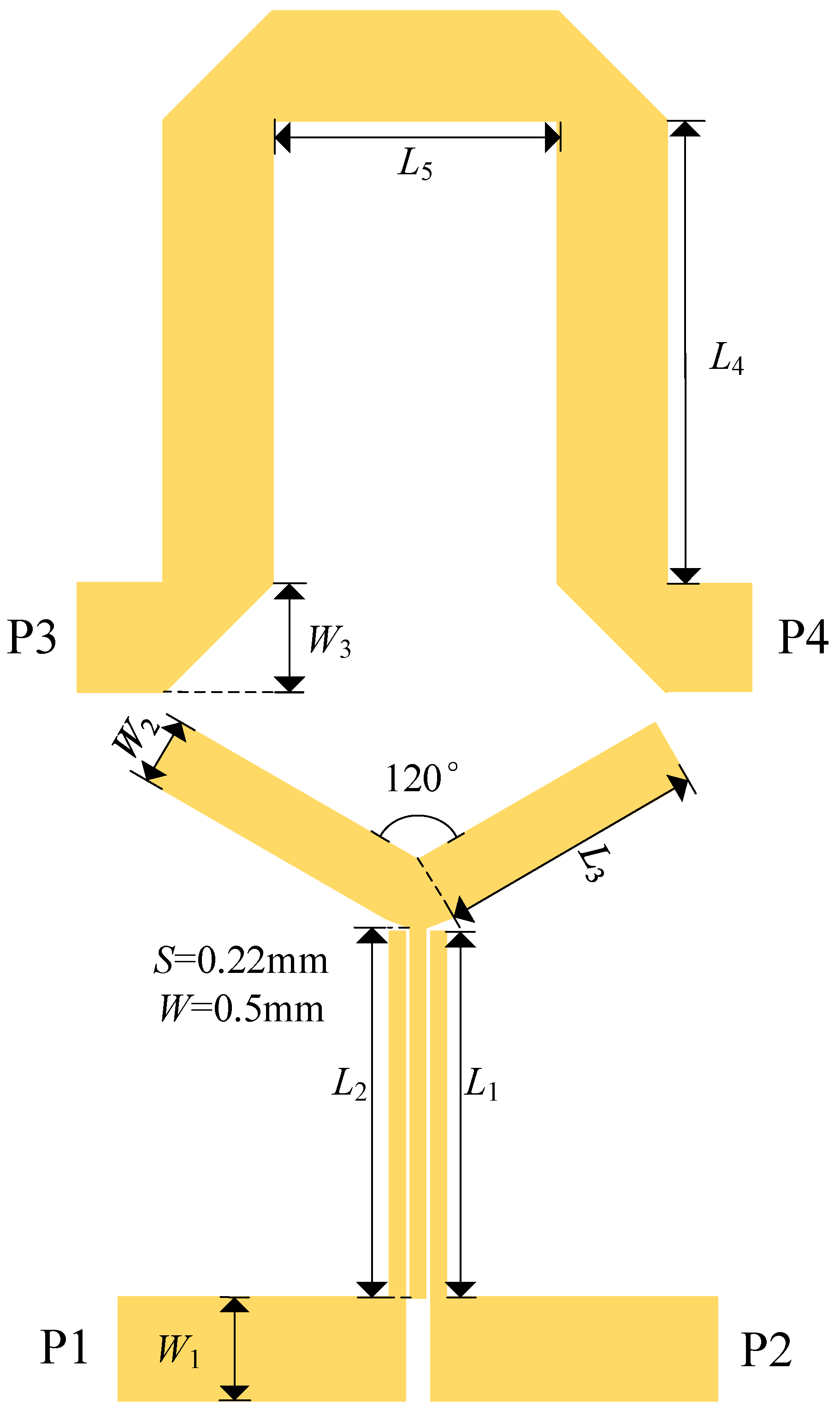
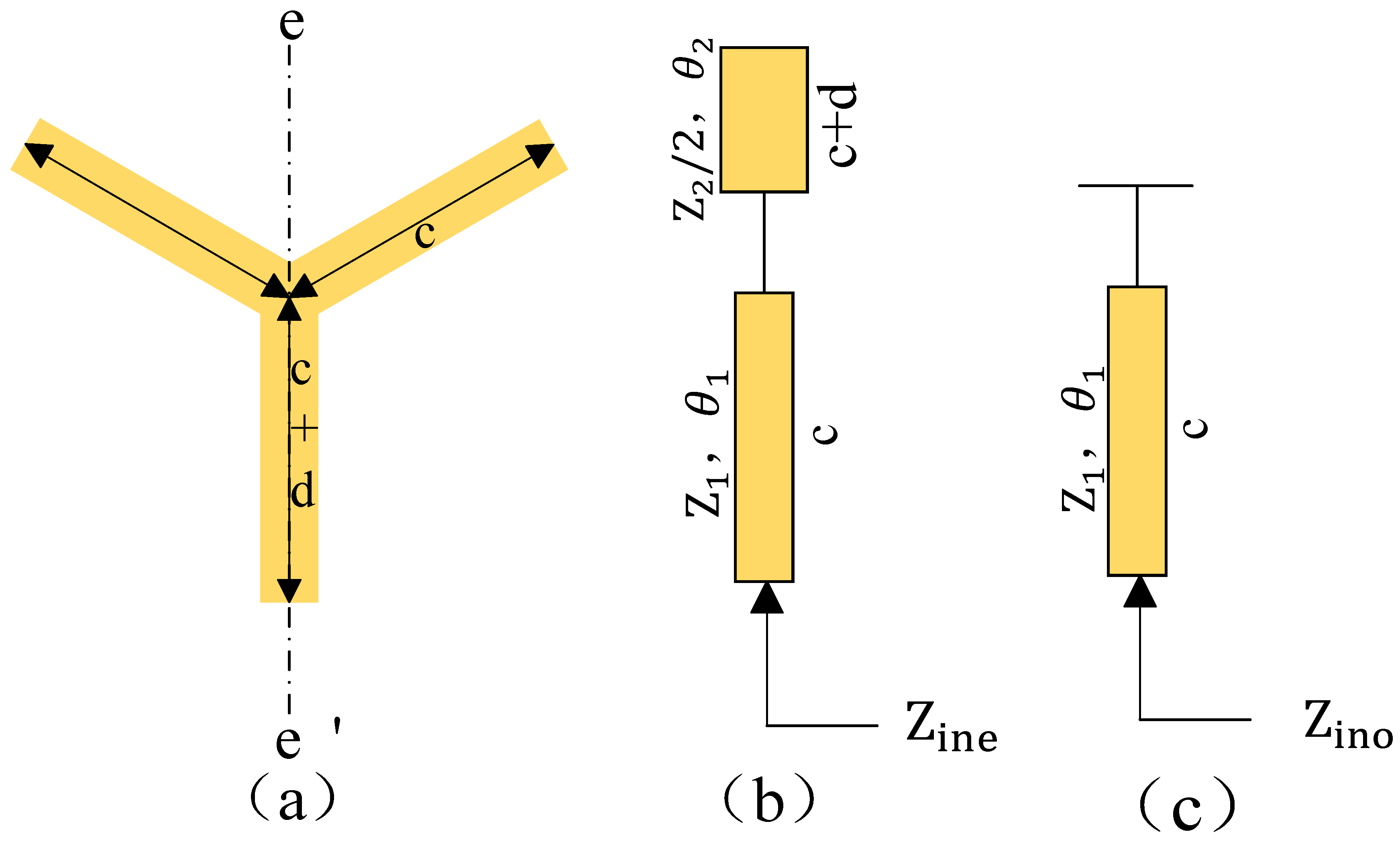
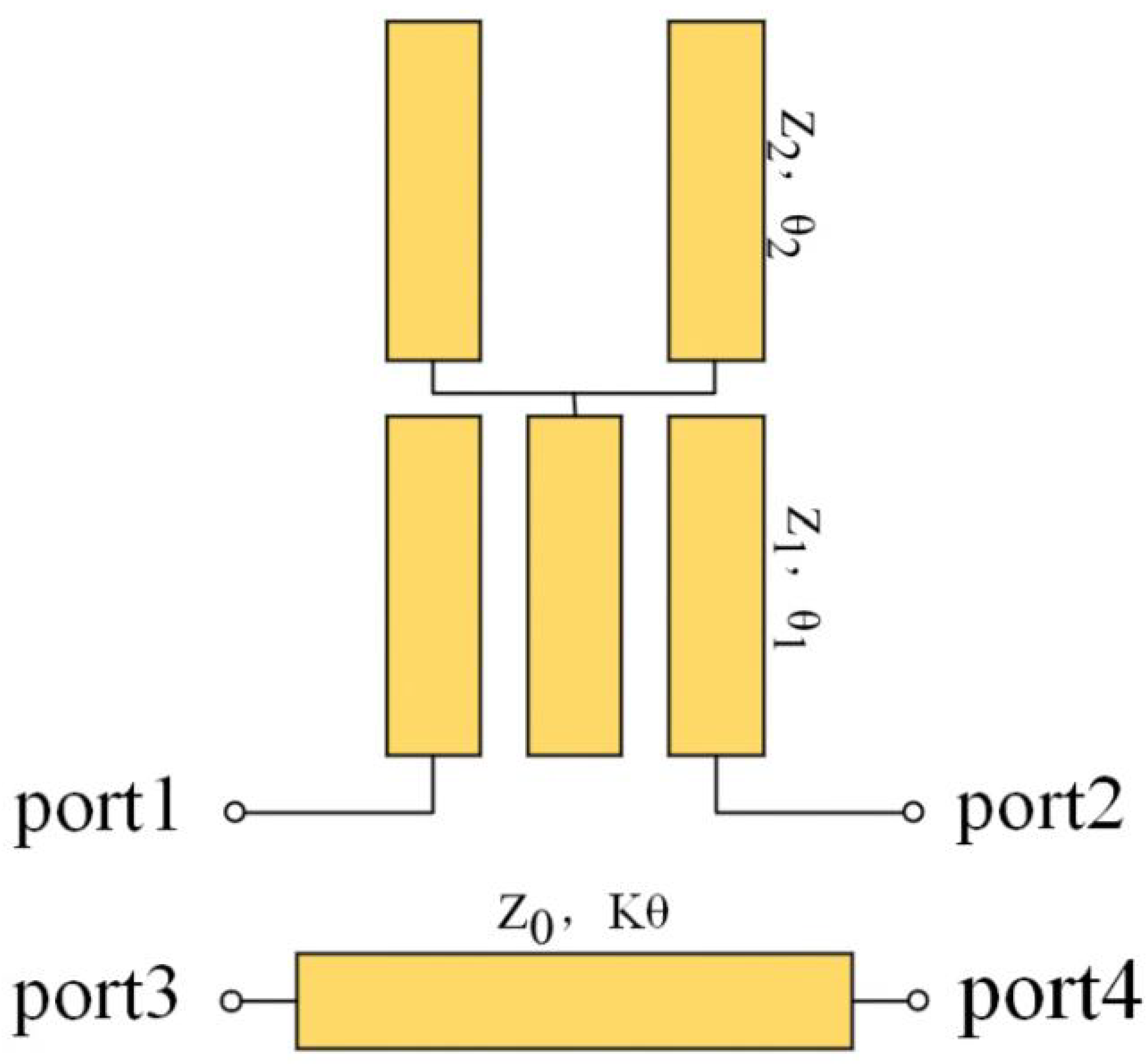
2. Proposed Structure

The topology of the proposed Y-type dual-mode microstrip phase shifter is shown in Figure 1. The Y-type dual-mode resonator is used in this novel structure. This dual-mode resonator consists of three microstrip lines connected at 120° intervals, with the left branch equal to the right branch. There is cross-coupling between port 1 and port 2, and there are two paths for signal transmission from port 1 to port 2: one is that the signal from port 1 is coupled to the Y-shaped resonator mainly through the parallel coupled line structure; the other is that a weak-end coupled direct signal path is formed through the input/output feeder roots. This coupling structure allows the filter to produce two finite transmission zeros in the upper and lower stop bands, resulting in a quasi-elliptic function response. The quasi-elliptical response combines the high selectivity of elliptical filters with the equal-ripple characteristics of the passband. However, unlike an ideal elliptical filter, the quasi-elliptical response can exhibit unequal amplitude ripple outside the band. This design enhances out-of-band rejection by introducing transmission zeros at the edges of the passband while also preserving better signal integrity within the passband. This response improves passband and out-of-band performance. The reference line is usually a uniform transmission line, and the phase shift of the phase shifter is controlled by adjusting the electrical length of the reference line.
Figure 2 shows a schematic diagram of the Y-type microstrip dual-mode resonator with an odd–even mode resonance equivalent circuit. From Figure 2a, it can be seen that the resonator is symmetric about ee, the odd-mode excitation in the symmetry plane will be shorted, and the odd-mode resonance equivalent circuit is shown in Figure 2c. The characteristic impedance can be defined as follows:
Z i n o = j Z 1 c o t θ 1 .
Here, θ 1 = β c is the electrical length of the Y-resonator branch, and the odd-mode resonance frequency f 0 can be obtained from the resonance condition that the odd-mode resonance derivative is zero:
f 0 = c 4 L 3 ε e .
For even-mode excitation, no current flows in the symmetry plane, and the even-mode resonant equivalent circuit is shown in Figure 2b. Using the transmission line theory and neglecting the effect of junction discontinuity, the characteristic impedance can be defined as follows:
Z i n e = j Z 1 2 t a n θ 1 t a n θ 2 Z 1 Z 2 2 Z 2 t a n θ 1 + Z 1 t a n θ 2 .
Here, θ 2 = β ( c + d ) is the electrical length of the main branch of the Y-type resonator, and the even-mode resonant frequency f e exists from the resonance condition where the even-mode resonant derivative is zero:
f e = c 4 L 2 ε e .
According to Equations (2) and (4), the appropriate branch lengths can be selected to obtain two appropriate resonant frequencies.

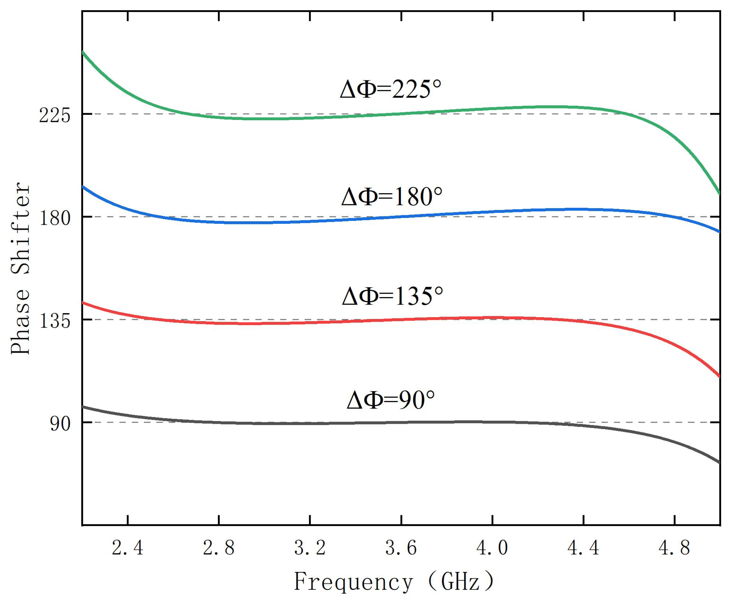
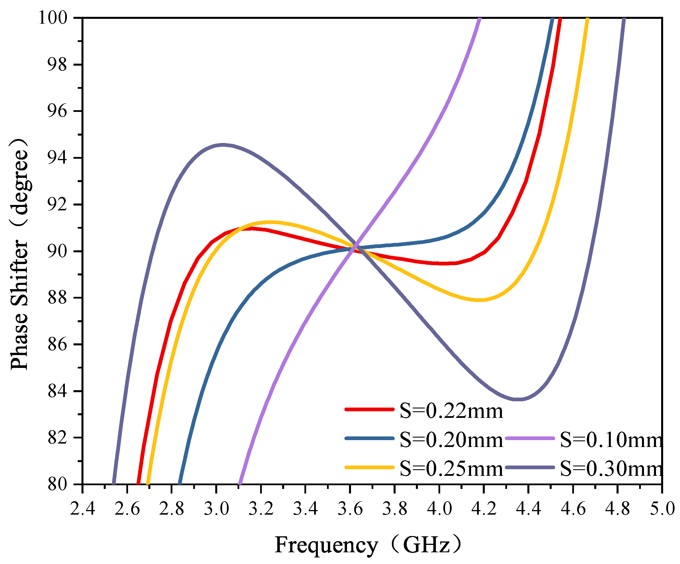
3. Analysis and Design

Figure 3 shows the schematic diagram of the equivalent circuit of the proposed phase shifter, where port 1 to port 2 are the main lines and port 3 to port 4 are the reference lines. The phase shift value of the phase shifter is the difference in the inserted phase shift between the main lines and the reference lines:
Δ Φ = Δ Φ m Δ Φ r ,
where Δ Φ m is the main line insertion phase shift, and Δ Φ r is the reference line insertion phase shift. According to the microwave network theory, the main and reference line insertion phase shifts of the phase shifter can be represented by the ABCD matrix as follows:
Δ Φ m = S 21 = t a n 1 B + C Z 0 2 j ( A + D ) Z 0 2 ,
Δ Φ r = S 43 = K θ .
In order to keep the phase shift value constant for a certain pass band of phase shift values, the phase slopes of the main and reference lines should be the same, i.e.,
d Δ Φ m d f f = f 0 = d Δ Φ r d f f = f 0 = K θ 0 f 0 .
For an ideal phase shifter, the phase difference between the main line and the reference line is constant over a frequency range, i.e., the phase shift value is constant. In practice, the phase difference between the two is somewhat variable over a range of operating frequencies. Assuming that the calibration phase shift value is Δ Φ 0 , the maximum phase shift value in the working band is Δ Φ m a x , and the minimum phase shift value is Δ Φ m i n . As shown in Figure 4, the phase deviation (PD) is defined as the maximum difference between the phase shift value and the calibration phase shift value in the working band:
P D = m a x Δ Φ m a x Δ Φ 0 , Δ Φ m i n Δ Φ 0 .
The schematic simulation results show that the proposed microstrip phase shifter can achieve a stable phase shift value of 225° over the operating bandwidth within the phase deviation PD. The reflection and transmission coefficients can be expressed as follows:
S 11 = Γ e + Γ o 2 ,
S 21 = Γ e Γ o 2 ,
where Γ e and Γ o denote the odd-mode reflection coefficient and even-mode reflection coefficient, respectively, with respect to the odd/even-mode input impedance:
Γ e = Z i n e Z 0 Z i n e + Z 0 ,
Γ o = Z i n o Z 0 Z i n o + Z 0 .
The parity mode input impedance in (1) and (3) is brought into (12) and (13) to yield the parity mode reflection coefficients, and then into (10) and (11) to yield the S-parameters. The ABCD matrix of the main line is obtained from (6):
2 j z 1 z 2 t a n θ 1 2 2 j z 1 z 2 2 z 1 2 z 2 t a n θ 1 z 1 3 t a n θ 1 2 t a n θ 2 2 z 2 t a n θ 1 + z 1 t a n θ 2 2 j z 1 2 t a n θ 1 t a n θ 2 .
The phase shift value Δ Φ can be obtained by bringing the required S-parameters into (6) and (7), and the transfer function F of the phase shift network is expressed as follows:
| S 21 | 2 = 1 1 + | F | 2 and F = B C 2 .
The transfer function F can be found by bringing the ABCD matrix of the phase shift network into the above equation. For the reference line, its ABCD matrix is, according to microwave theory, as follows:
c o s K θ j z 0 s i n K θ j s i n K θ z 0 c o s K θ .
The ABCD matrix of the reference line is brought into Equation (6) to obtain the insertion phase shift of the reference line and, hence, the phase shift value of the phase shifter. The phase response for different phase shift values is shown in Figure 5. The phase shifter proposed in this paper achieves wide broadband and low phase deviation for different values of phase shift. It can be seen from the figure that the phase deviation increases gradually as the phase shift value increases from 90° to 225°. When the phase shift value is 90°, the fractional bandwidth can reach 60.8%, and its phase deviation is less than 1.2°. A wide bandwidth can be realized with a smaller phase deviation and a simpler structure. In general, the phase response of a wideband phase shifter is highly sensitive to the coupling distance. Figure 6 illustrates the relationship between coupling distance and phase response, indicating that as the coupling distance decreases, both the phase shift bandwidth and phase shift deviation reduce. Conversely, increasing the coupling distance leads to a broader phase shift bandwidth but also increases the phase shift deviation. Specifically, when the coupling distance is set to S = 0.20 mm, the phase shift bandwidth becomes too small. At S = 0.25 mm, while the phase shift bandwidth increases, the phase shift deviation exceeds 2°, which does not align with the design objectives. After carefully balancing the phase shift bandwidth and deviation, the optimal coupling distance is determined to be S = 0.22 mm.

Design Steps

The design flow chart is shown in Figure 7: (1) Draw the corresponding odd-mode and even-mode circuits based on the structure of the proposed filter phase shifter; (2) Using your knowledge of microwave theory, write the input impedances corresponding to an odd-mode circuit and an even-mode circuit, noted as Z i n o and Z i n e ; (3) Find the S-parameters from the reflection and transmission coefficients with respect to the odd/even input impedance with the ABCD matrix; (4) Write the reflection coefficient S 11 , transmission coefficient S 21 , and insertion phase of the network based on the conversion relationship between the ABCD matrix and the scattering parameter; (5) The insertion phases of the main and reference networks are operated as a difference to derive the phase shift value Δ Φ ; (6) First-order differentiation of the insertion phase such that the slopes of the insertion phases of the two networks are the same in the operating frequency band; (7) Determine component parameter values using | S 11 | = 0 , | S 21 | = 1 , and steps (5) and (6); (8) Based on the parameters of the selected dielectric substrate (substrate thickness, dielectric constant, and loss angle tangent), the calculated circuit parameters (characteristic impedance and electrical length) are converted to actual physical dimensions using closed-form equations; (9) The physical dimensions of the phase shifter are slightly adjusted using simulation software. With this design step, the designed 90°, 135°, 180°, and 225° equivalent circuit parameters, as well as physical dimensions, can be obtained, as shown in Table 1.

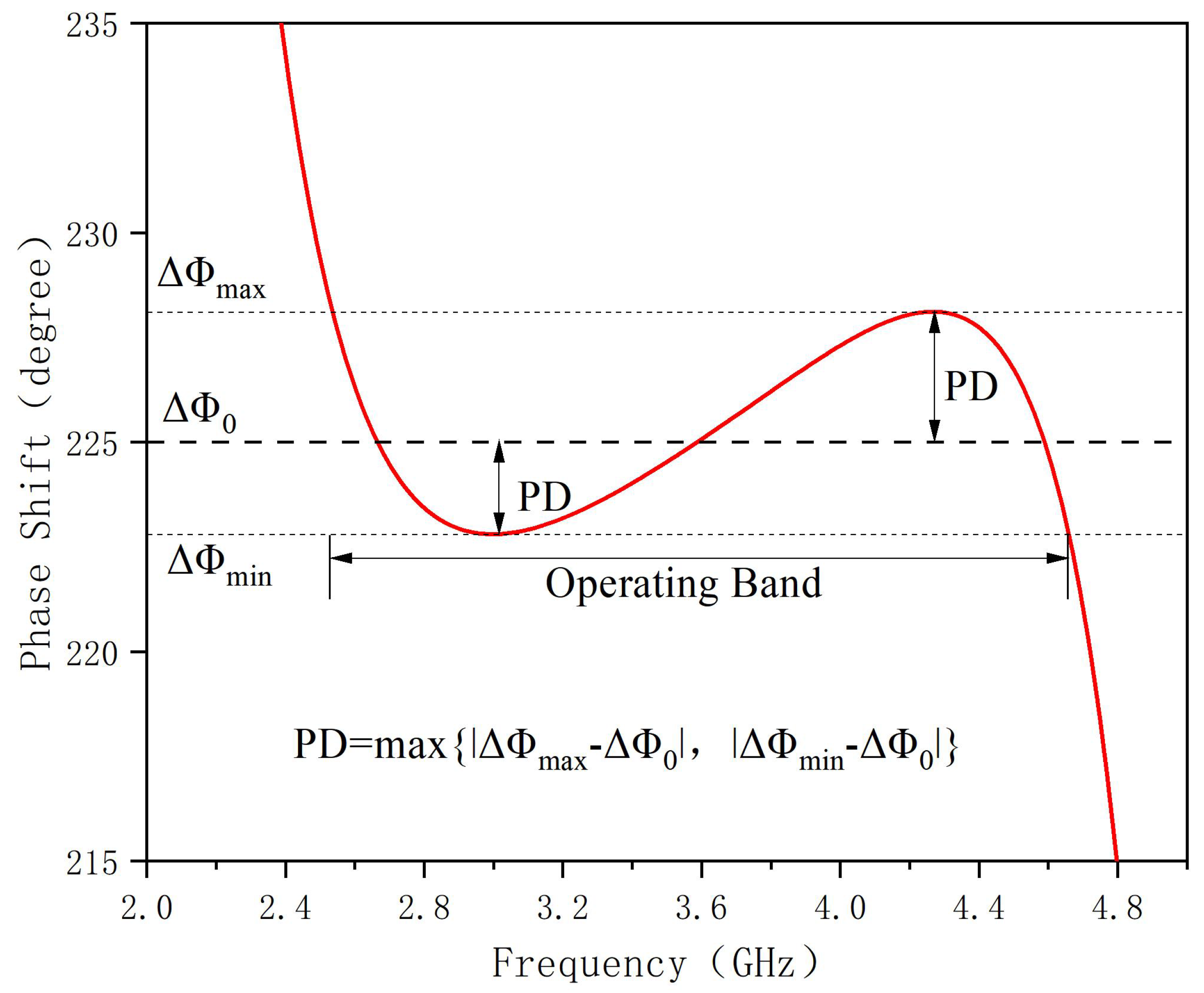
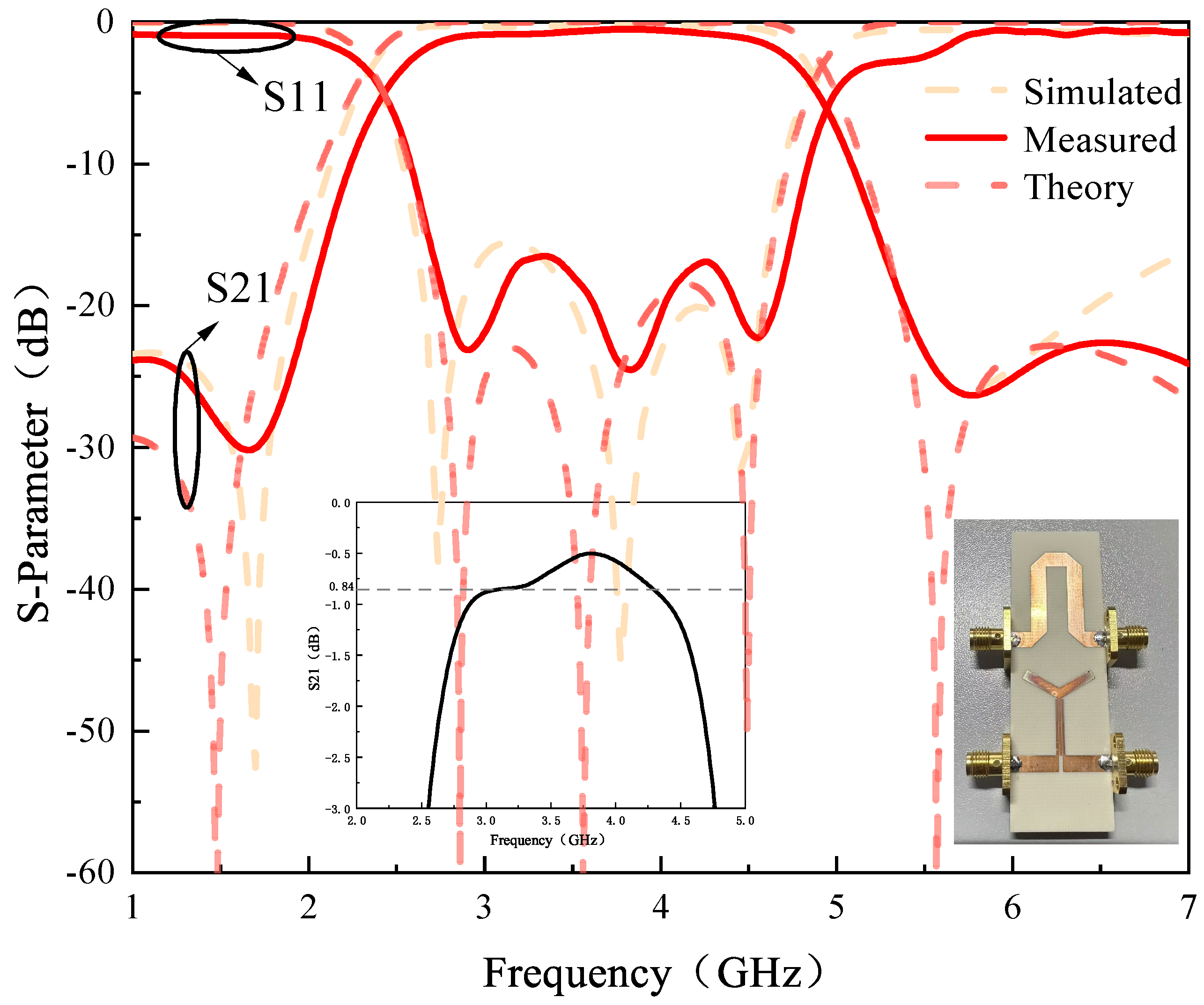
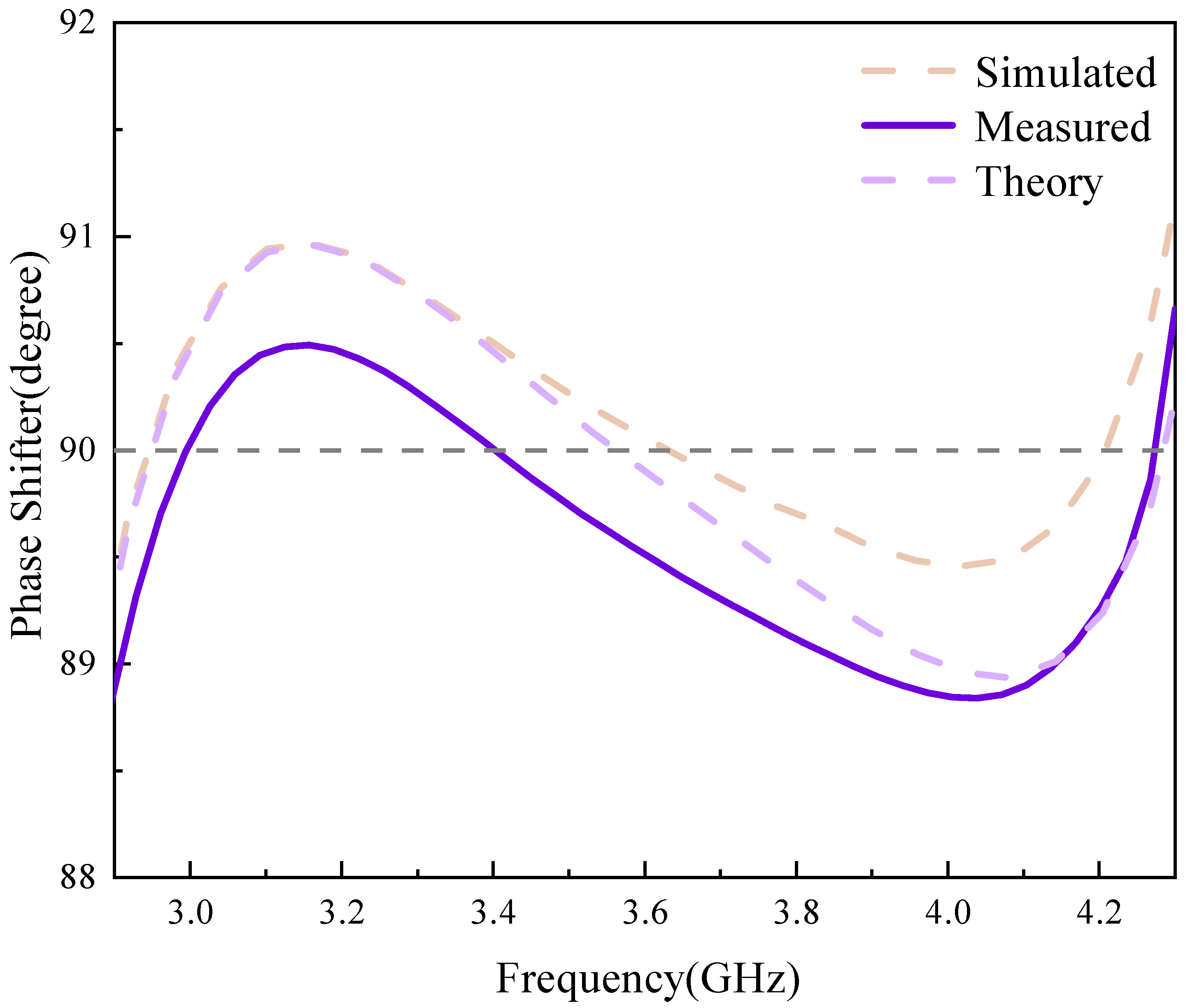
4. Result and Discussion

In order to demonstrate the proposed phase shifter, a broadband phase shifter with a center frequency of 3.6 GHz, a relative bandwidth of 60.8%, and a phase shift of 90° are designed and fabricated. The proposed phase shifter is realized on a single-layer microstrip structure. The substrate used is Rogers 4003 (ϵr = 3.55, tanδ = 0.0027, h = 1.524 mm). After further analysis and optimization using ADS2020 software, the instrument used for the measurements was a Ceyear 3672C. The final layout of the phase shifter is shown in Table 1, and the processing test shot is shown in Figure 8.
The magnitude response and phase response of the designed microstrip phase shifter are shown in Figure 8 and Figure 9. From Figure 8, it can be seen that the 3 dB bandwidth is 60.8% in the frequency range of 2.56–4.75 GHz, the minimum return loss is better than 16.5 dB, the insertion loss is less than 1.2 dB, and due to the use of input-output cross-coupling, two transmission zeros are introduced near the passband cutoff edge at 1.68 and 5.77. As can be seen in Figure 8, the phase shifter has a phase shift value of 90° ± 1.2° in the frequency range of 2.7–4.3. The measured results are largely consistent with both the schematic and layout simulation results. However, because the physical connections at the SMA interface and solder joints are idealized in the simulation, this can lead to slight variations in the resonant frequency, resulting in a measured frequency response that displays minor multiple resonances. To facilitate comparison with other reported studies, Table 2 has been prepared. It clearly shows that the phase error, insertion loss, return loss, and relative bandwidth in [5,9] are inferior to those of the current phase shifter. In [6], the alignment of the center frequency with the current phase shifter is more informative; although its insertion loss (better than 0.6) surpasses that of the current phase shifter (better than 0.84), its phase error, return loss, and relative bandwidth are not as favorable. This highlights the excellent phase shift accuracy of the proposed phase shifter. The phase shift range in [8] can achieve 0–360°, and its insertion loss and relative bandwidth are slightly superior to those of the current phase shifter. However, with a phase error of up to 10°, the advantage of the current phase shifter in terms of minimal phase error becomes more pronounced. Furthermore, the phase shift range and phase error in [10,16] do not match those of the current phase shifter. While the insertion loss, return loss, and relative bandwidth in [10] are better, the complexity of its structure makes processing and fabrication more challenging than for the current phase shifter.

5. Conclusions

In this paper, a phase shifter using a Y-type resonator was proposed and theoretically and experimentally investigated. The proposed microstrip line phase shifter has the advantages of small phase error, wide operating bandwidth and simple structure. In addition, this paper presented a design methodology that allows one to directly determine the initial physical dimensions of the phase shifter based on the specified specifications. Based on this synthesis method, a 90° phase shifter with a bandwidth of 60.8% and a phase deviation of 1.2° was realized.

Author Contributions

Conceptualization, X.F. and Y.M.; methodology, Y.M.; software, Y.M.; validation, Y.M. and X.F.; formal analysis, Y.M.; investigation, X.F.; writing—original draft preparation, Y.M.; writing—review and editing, Y.M.; visualization, W.X.; supervision, L.F. and T.L.; project administration, Y.M.; funding acquisition, X.F. and H.C. All authors have read and agreed to the published version of the manuscript.

Funding

This paper is the research result of the project funded by Guangxi Natural Science Foundation for Distinguished Youth (2023GXNSFFA026002) and Liuzhou Science and Technology Program for Research and Application of Remote Intelligent Remote Control Construction Machinery (2022AAB0101).

Data Availability Statement

The original contributions presented in the study are included in the article, further inquiries can be directed to the corresponding author.

Conflicts of Interest

The authors declare no conflicts of interest.

References

  1. Tolin, E.; Vipiana, F.; Litschke, O.; Bruni, S. Phase shifters design for scan range extension of Rotman lens beamforming based antenna arrays. In Proceedings of the 2018 IEEE International Symposium on Antennas and Propagation & USNC/URSI National Radio Science Meeting, Boston, MA, USA, 8–13 July 2018; IEEE: Piscataway, NJ, USA, 2018; pp. 2129–2130. [Google Scholar]
  2. Kobayashi, A.; Imanishi, R.; Nosaka, H. Fast-Phase-Switching Current-Mode Phase Shifter for Beyond 5G Phased Array Antenna. In Proceedings of the 2023 53rd European Microwave Conference (EuMC), Berlin, Germany, 19–21 September 2023; IEEE: Piscataway, NJ, USA, 2023; pp. 26–29. [Google Scholar]
  3. Cao, J.Z.; Chen, F.C. Design of continuously steerable Nolen matrix-based beamforming networks using tunable phase shifters. In Proceedings of the 2022 International Conference on Microwave and Millimeter Wave Technology (ICMMT), Harbin, China, 12–15 August 2022; IEEE: Piscataway, NJ, USA, 2022; pp. 1–3. [Google Scholar]
  4. Qiu, L.L.; Zhu, L. Synthesis design of filtering differential phase shifters of independently suppressed harmonics. IEEE Trans. Circuits Syst. II Express Briefs 2021, 68, 2760–2764. [Google Scholar] [CrossRef]
  5. Xu, W.; Li, T.; Chen, X.; Chen, H.; Feng, L. Highly selective phase shifter using stub-loaded coupled-line resonators. Microw. Opt. Technol. Lett. 2023, 65, 3164–3170. [Google Scholar] [CrossRef]
  6. Tian, Y.; Gu, J.; Xu, H.; Liu, W.; Duan, Z.; Gao, H.; Yan, N. A 26-32GHz 6-bit bidirectional passive phase shifter with 14dBm IP1dB and 2.6° RMS phase error for phased array system in 40nm CMOS. In Proceedings of the 2023 IEEE/MTT-S International Microwave Symposium-IMS 2023, San Diego, CA, USA, 11–16 June 2023; IEEE: Piscataway, NJ, USA, 2023; pp. 195–198. [Google Scholar]
  7. Jang, Y.; Salman, M.; Jeong, Y.C.; Choi, K.S.; Han, S.M.; Ahn, D. Wideband phase shifter using 3 types of LC resonant circuits for phase slope alignment. In Proceedings of the 2019 PhotonIcs & Electromagnetics Research Symposium-Spring (PIERS-Spring), Rome, Italy, 17–20 June 2019; IEEE: Piscataway, NJ, USA, 2019; pp. 4034–4039. [Google Scholar]
  8. Lyu, Y.P.; Zhu, L.; Cheng, C.H. Design and analysis of Schiffman phase shifter under operation of its second phase period. IEEE Trans. Microw. Theory Tech. 2018, 66, 3263–3269. [Google Scholar] [CrossRef]
  9. Feng, L.; Chen, J.; Yu, X.; Zhu, L.; Liu, H. A novel wideband 90° filtering phase shifter using broadside-coupled MSLs. IEEE Trans. Circuits Syst. II Express Briefs 2022, 69, 2742–2746. [Google Scholar] [CrossRef]
  10. Zheng, B.; Tang, H.; Li, H.; Zhou, L.; Dong, Y.; Haerinia, M.; Zhang, H. Ultra-Wideband Schiffman Phase Shifter Designed with Deep Neural Networks. Authorea Prepr. 2023. [Google Scholar]
  11. Qiu, L.L.; Zhu, L.; Lyu, Y.P. Schiffman phase shifters with wide phase shift range under operation of first and second phase periods in a coupled line. IEEE Trans. Microw. Theory Tech. 2019, 68, 1423–1430. [Google Scholar] [CrossRef]
  12. Zheng, S.Y.; Chan, W.S. Differential RF phase shifter with harmonic suppression. IEEE Trans. Ind. Electron. 2013, 61, 2891–2899. [Google Scholar] [CrossRef]
  13. Yeung, S.H.; Xue, Q.; Man, K.F. Broadband 90 Differential Phase Shifter Constructed Using a Pair of Multisection Radial Line Stubs. IEEE Trans. Microw. Theory Tech. 2012, 60, 2760–2767. [Google Scholar] [CrossRef]
  14. Zheng, S.Y.; Chan, W.S.; Man, K.F. Broadband phase shifter using loaded transmission line. IEEE Microw. Wirel. Components Lett. 2010, 20, 498–500. [Google Scholar] [CrossRef]
  15. Tang, X.; Mouthaan, K. Phase-shifter design using phase-slope alignment with grounded shunt λ/4 stubs. IEEE Trans. Microw. Theory Tech. 2010, 58, 1573–1583. [Google Scholar] [CrossRef]
  16. Wang, Y.; Bialkowski, M.; Abbosh, A. Double Microstrip-Slot Transitions for Broadband 90° Microstrip Phase Shifters. IEEE Microw. Mireless Components Lett. 2012, 22, 58–60. [Google Scholar] [CrossRef]
  17. Lyu, Y.P.; Zhu, L.; Cheng, C.H. A new design of ultrawideband single-layer 90° phase shifter in the view of group delay. IEEE Microw. Wirel. Components Lett. 2019, 29, 376–378. [Google Scholar] [CrossRef]
  18. Dong, Q.; Wu, Y.; Zheng, Y.; Wang, W.; Liu, Y. A compact single-layer ultra-wideband phase shifter using weakly coupled lines. IEEE Access 2019, 7, 12575–12583. [Google Scholar] [CrossRef]
  19. Liu, H.; Zhang, L.; Pan, J.; Guo, Y.; Dai, X. Design of a wideband phase shifter using loaded element. In Proceedings of the 2016 Progress in Electromagnetic Research Symposium (PIERS), Shanghai, China, 8–11 August 2016; IEEE: Piscataway, NJ, USA, 2016; pp. 2153–2155. [Google Scholar]
Figure 1. Topology of the Y-type dual-mode microstrip phase shifter.
Electronics 13 05006 g001
Figure 2. Schematic diagram of the Y-type microstrip dual-mode resonator with a parity mode resonance equivalent circuit. (a) Y-Resonator Topology (b) Even-mode resonant equivalent circuit (c) Odd mode resonance equivalent circuit.
Electronics 13 05006 g002
Figure 3. Equivalent schematic of the proposed wideband phase shifter.
Electronics 13 05006 g003
Figure 4. Phase shift response between main and reference lines.
Electronics 13 05006 g004
Figure 5. Phase response for four different phase shift values.
Electronics 13 05006 g005
Figure 6. Phase shift response for different coupling distances.
Electronics 13 05006 g006
Figure 7. Phase response for four different phase shift values.
Electronics 13 05006 g007
Figure 8. Frequency response of theoretical, simulated, and measured results.
Electronics 13 05006 g008
Figure 9. Phase response of theoretical, simulated, and measured results.
Electronics 13 05006 g009
Table 1. Equivalent circuit parameters as well as physical dimensions for the four designed phase shift values.
Phase Shifter (°)Equivalent Circuit Parameters (°\ohm)Physical Dimensions (mm)
90Z0 = 50; Z1 = 51.2; Z2 = 92.4; θ 1 = 84; θ 2 = 76.2; K = 0.482; θ = 226.1L1 = 12.8; L2 = 12.95; L3 = 9.6;
L4 = 16.2; L5 = 10; W1 = 3.6;
W2 = 2.3; W3 = 3.8; S = 0.22
135Z0 = 50; Z1 = 50.7; Z2 = 91.5; θ 1 = 91.5; θ 2 = 69.2; K = 0.469; θ = 141.4L1 = 15.5; L2 = 15.8; L3 = 10;
L4 = 15.2; L5 = 10; W1 = 3.6;
W2 = 1; W3 = 3.8; S = 0.15
180Z0 = 50; Z1 = 72.8; Z2 = 92.4; θ 1 = 87.8; θ 2 = 76.2; K = 0.403; θ = 176.1L1 = 14; L2 = 14.2; L3 = 11;
L4 = 15.2; L5 = 10; W1 = 3.6;
W2 = 1; W3 = 3.8; S = 0.09
225Z0 = 50; Z1 = 94.6; Z2 = 92.4; θ 1 = 92; θ 2 = 76.2; K = 0.412; θ = 226.1L1 = 14; L2 = 15.1; L3 = 11;
L4 = 18.2; L5 = 10; W1 = 3.6;
W2 = 2.3; W3 = 3.8; S = 0.205
Table 2. Parameters of the proposed phase shifter with small phase error.
ReferenceF0 (GHz)PR (°)MaxPD (°)IL/RL (dB)FBW (%)
50.589.9±1.5<1.4/>1637.5
63.645–180±5<0.6/>1538.5
82.250–360±10<0.5/>1064
9390±2.8<1.2/>1058
10390±3<0.46/>2280
17390±3<0.97/>19.660.3
This Work3.690–225±1.2<0.84/>16.560.8
Disclaimer/Publisher’s Note: The statements, opinions and data contained in all publications are solely those of the individual author(s) and contributor(s) and not of MDPI and/or the editor(s). MDPI and/or the editor(s) disclaim responsibility for any injury to people or property resulting from any ideas, methods, instructions or products referred to in the content.

