1. Introduction
The microcontroller unit (MCU) serves as a core component in the field of automotive electronics. With the global increase in the electric vehicle industry, there is heightened demand for advanced MCU features, performance, Design For Test (DFT) considerations, and efficient chip probing (CP) testing strategies for mid- to high-end automotive MCUs. Among these, Flash embedded within automotive-grade MCUs stands out as a critical module [
1]. Notably, the mass production CP testing cost of these MCUs is dominated by the Flash component, accounting for approximately 70% to 80% of the overall MCU test cost. For instance, in the case of a 40 nm MCU Flash, the CP testing cost per 10,000 wafers can reach USD 1 to 2 million. Reducing the testing time by even 10% could yield substantial cost savings, potentially lowering expenses by USD 100,000 to 200,000.
The stringent requirements for internal voltage and current within the Flash macro of automotive-grade MCUs necessitate precise trimming during CP testing. Specifically, Flash ESF3 cells require the measurement of three types of high-voltage analog signals: voltage of erase gate (VEG), voltage of coupling gate (VCG), and voltage of source line (VSL). Each measurement involves selecting from 24 different trimming levels. Notably, the trimming of high-voltage analog signals accounts for nearly 7% of all CP1 testing times, often representing an efficiency bottleneck in automated test equipment (ATE) measurements. Consequently, specialized ATE [
2] and versatile Built-In Self-Test (BIST) [
3,
4,
5] modes are essential for handling various high-voltage and current trimming requirements.
Upgrading existing hardware resources for widely used mass-production ATE devices remains a formidable challenge, particularly due to the constraints often imposed by budget, physical space, and compatibility issues. Therefore, under unchanged hardware conditions, accelerating the measurement speed of high-voltage analog quantities during CP testing emerges as a pivotal aspect of enhancing CP efficiency. To achieve this goal, effective strategies must encompass not only the enhancement of the concurrent testing capability of embedded Flash within the MCU, but also the optimization of the testing efficiency of individual Flash components.
The existing literature has explored various methods that address these challenges. The authors of reference [
6] have focused on the software and hardware design of embedded channel ATE. They provided efficient ATE for chip testing, but without involving the circuit design of BIST. The authors of reference [
7] meticulously aligned ATE resources, including power supplies, high-voltage generators, and digital interfaces, with the specific requirements of MCU Flash testing. They also innovatively compressed and integrated a dedicated BIST instruction set. This compression enables MCU-side decoding, drastically reducing the additional system overhead. Through offloading some of the processing tasks to the MCU itself, this approach streamlines the testing process and further accelerates test speeds. The authors of reference [
8] have improved CP test efficiencies through an adaptive test algorithm, yet they did not optimize the actual BIST design or equipment measurement process. Multiple BIST engines have been employed in [
9] to achieve the concurrent testing of multiple IPs within the SoC, optimizing test times compared to the serial testing of IPs. However, the detailed test items for different types of IPs were not further optimized, especially the time-consuming analog trimming test items. The authors of reference [
10] have completed the auto-trimming of multiple analog voltages in the multi-core RF SoC through the internal design of multiplexers and ADCs, improving test efficiencies. Nevertheless, adding ADCs in the DFT circuit significantly increases the chip area due to testing. Moreover, the authors of [
11] have improved the auto-trimming system of the embedded Flash reference current source in the MCU by establishing and optimizing the MCU internal current measurement unit, achieving mass production test efficiency improvements. However, this requires the design of complex current measurement units in the MCU.
All aforementioned methods mainly rely on existing ATE for the actual testing process, necessitating the use of ATE measurement units specifically designed for high-voltage analog testing. However, this reliance introduces additional time overhead due to the need for setup, calibration, and resource allocation. To address this limitation and ensure measurement accuracy without ATE involvement, this study proposes an auto-trimming-based DFT optimization method. By maintaining the original embedded Flash structure, we introduce a high-precision voltage comparison module within the MCU. Simultaneously, corresponding digital logic is added to the BIST circuitry, enabling the rapid and precise automatic trimming of the aforementioned voltage signals, significantly reducing testing time.
The study is organized as follows:
Section 2 shows the proposed auto-trimming-based DFT without using ATE measurements, and the implementation is provided in
Section 3. The experimental setup and results are detailed in
Section 4 and
Section 5, respectively.
Section 6 concludes the study.
2. Proposed Auto-Trimming-Based DFT Without Using ATE Measurements
As shown in
Figure 1, the conventional analog trimming methods involve direct ATE measurements of the high-voltage analog signals (VPP0/1) within the Flash component. The BIST (Built-In Self-Test) mechanism controls the Flash macro to adjust the voltage. For embedded Flash, the HV (high-voltage) output requires entry into the Flash’s test mode. In this mode, analog switches control the output voltages: VEG, VCG, and VSL; moreover, trimming registers are configured to adjust the voltage. ATE measurements are then used to ensure that the output meets the desired target.
At present, there are two strategies for measuring high-voltage analog signals during the CP process. The first involves traversing all possible trimming codes and selecting the one corresponding to the target value. The second strategy accelerates trimming using a binary search approach. However, both methods rely on ATE involvement for analog measurements, resulting in frequent calls to ATE devices and significantly reducing the measurement speed. For instance, when measuring a 1 MB Flash macro using a T5830 (Advantest, Tokyo, Japan) ATE device, the ATE completes the measurement of the three analog signals in approximately 2.94 s, accounting for approximately 7% of the total MCU testing time of 42.65 s.
Without relying on the measurement unit of ATE, with the measurement completed inside the chip, automated trimming can be realized within the chip. This will shorten testing times and reduce testing costs simultaneously. To achieve this goal, two aspects of design optimization are needed: increasing the relevant BIST instruction set to complete the process control of automated trimming. Moreover, adding an analog module for automated voltage measurement can be achieved by adding an on-chip ADC for voltage measurements, but this method requires a more complex ADC IP and occupies a larger chip area.
As depicted in
Figure 2, the proposed auto-trimming method eliminates the need for ATE in analog measurements. The entire measurement process is self-contained within the chip, achieving the automatic trimming of analog signals. Specifically, the analog signal VPP0/1 from the Flash component connects to the BIST module. Instead of directly measuring the signal, the ATE provides a reference voltage. The BIST module then controls the Flash macro to adjust the voltage while simultaneously evaluating the trimming outcome.
3. Implementation of Proposed Auto-Trimming-Based DFT Without Using ATE Measuring
The entire system of the proposed auto-trimming-based DFT without using ATE measurement includes analog and digital module designs. The analog module consists of two high-precision comparators, as shown in
Figure 3, and the digital module is shown in
Figure 4.
As shown in
Figure 3, when the CP tests the trimming item of the embedded high-voltage Flash module, the ATE machine must first provide two reference voltages. The specific value of the reference voltage needs to be determined according to the trimming target and the voltage division situation. The reference voltage is directly used as the input of the comparator, and the other end of the comparator is input by the high-voltage Flash module that needs trimming after voltage division. The ATE machine sends the auto-trimming command. Then, the digital module starts its operations. Moreover, the digital module configures the Flash Test Mode, and the configuration registers. Consequently, Vpp0/1 is output from the internal voltage division to the embedded Flash external pin Vpp0/1. Vpp0/1 is directly connected to the other end of the comparator. After comparison, the output is connected to the auto-trimming digital module in the BIST circuit. After two rounds of scanning, the digital module obtains the Trim code closest to the target value. The enabled signal of the comparator is given by auto-trimming. After the test is completed, the two comparators are disabled. To ensure normal operation in non-auto-trimming conditions, Vpp0/1 also needs to be connected to ATE to ensure that trimming can be carried out directly through ATE when entering debug mode.
As shown in
Figure 5, taking VEG voltage trimming as an example, the target range is 5.0 ± 0.06 V. Due to the code shifting accuracy of about 70 mV, the reference voltage accuracy range provided by ATE must be greater than 2–3 times the shifting accuracy to ensure that it is within the target range after shifting. The first round of Trim adjusts the gear from the top to the bottom in order to obtain codes. The second round comprises bottom-up gear shifting, resulting in codes. After obtaining two codes, the midpoint is taken to ensure that the trimming analog is closest to the target value. ATE is needed to supply a reference voltage serving as a voltage benchmark, and measurement accuracy hinges on the accuracy of the reference voltage provided by the mainstream Memory ATE. Moreover, the voltage output accuracy of mainstream Memory ATE (M2 (Teradyne, North Reading, MA, USA) and T5830) is from 250 μV to 2 mV, which can fully meet the current 70 mV accuracy requirement.
The digital BIST includes an SPI controller, Function controller, BIST controller, and other modules, which are specifically mounted on the internal bus of the Flash Interconnector; it is necessary to add corresponding auto-trimming processes on the internal bus to complete the automatic trimming of the Flash HV module. As shown in
Figure 4, the auto-trimming module is directly connected to the Flash Interconnector of the BIST circuit internally and to the SPI/JTAG controller module externally. It mainly includes three design sections:
- (1)
Input and output interface design, which is mainly divided into a system interface and SPI/JTAG controller interface.
- (2)
The state machine of the auto-trimming module, for which its state mainly carried out three major functions, including (a) controlling the Flash macro so that it enters the measurement mode of the relevant high-voltage analog signal; (b) controlling the analog comparator to obtain the comparison result between the trimming signal and the reference voltage provided by ATE; and (c) controlling the BIST circuit to enable it to output the trimming code and obtaining the comparison result from the analog comparator to make the final judgment on the completion of trimming.
- (3)
Instruction set system: In total, four sets of instructions are designed, namely, trimming from high to low voltages, trimming from low to high voltages, enabling/disabling the comparator, and reading the trimming code.
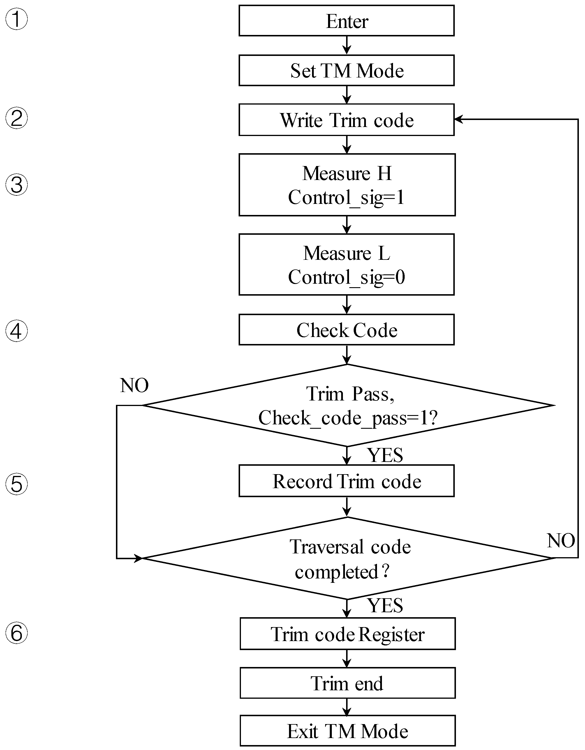
The specific process is shown in
Figure 6. ① First, the TM (Test Mode) of the embedded Flash is entered, and the measurement mode of VEG, VCG, and VSL is switched on. This step initializes the necessary test environment within the flash memory subsystem, allowing for subsequent measurement and trimming operations. ② The trimming code is written into Flash via BIST, and the voltage of the above measurement signal is adjusted. By using the Built-In Self-Test (BIST) mechanism, the trimming code can be precisely written to the Flash, and the associated voltages can be adjusted to the desired levels for accurate measurement. ③ A trimming voltage scan is performed, and it is compared with the voltage comparator to find the flip point of its output from 0 to 1, which is the Measure H step in the figure. Then, a reverse voltage scan is performed to find the flip point of the comparator from 1 to 0, which is the Measure L step in the figure. ④, ⑤, and ⑥ mainly confirm whether trimming is completed. If the target is achieved, the trimming code is recorded, and the TM (Test Mode) is exited. If the target is not achieved, trimming is continued. The accuracy of auto-trimming is related to the setting of the comparator’s reference voltage multiplied by the before and after values. The proper setting of these reference voltages is crucial as it determines the sensitivity and precision of the comparator in detecting the flip points during the Measure H and L steps, thereby directly influencing the overall accuracy of the auto-trimming process.
4. Experimental Test Setup
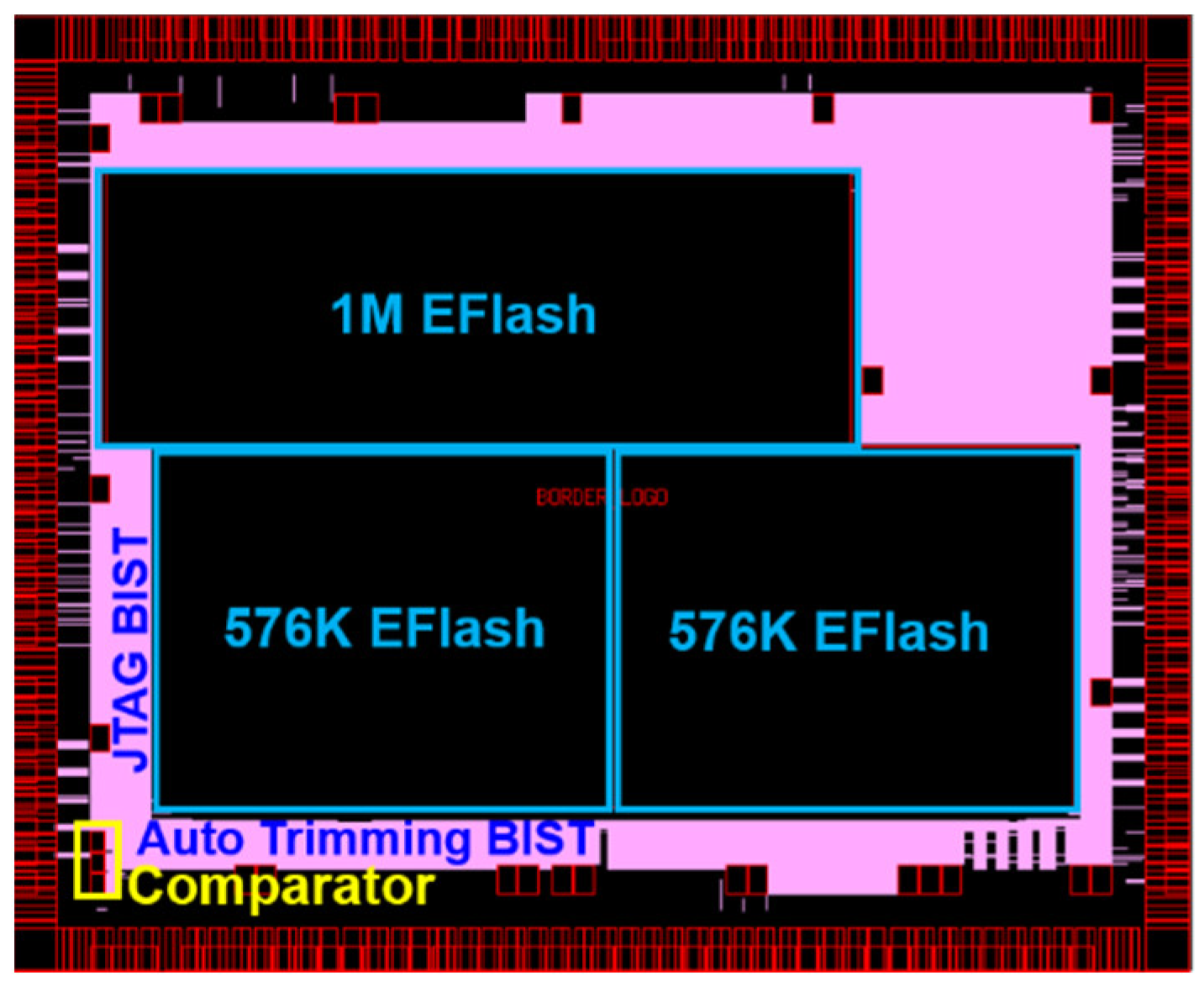
In order to verify the function, performance, and reliability of the auto-trimming embedded Flash BIST optimization design, a verification chip is designed. The architecture of the entire verification chip (Test Chip) is shown in
Figure 7.
The test environment setup is shown in
Figure 8. The wafer-level CP test solution is adopted. The hardware equipment uses the 93 K (Advantest, Tokyo, Japan) test machine, the probe station uses a fully automatic probe station, and the connection between the probe card and the ATE 93 K is connected via high-speed signal cables. The clock frequency of the test chip does not exceed 100 MHz, and an engineering cantilever probe card is used.
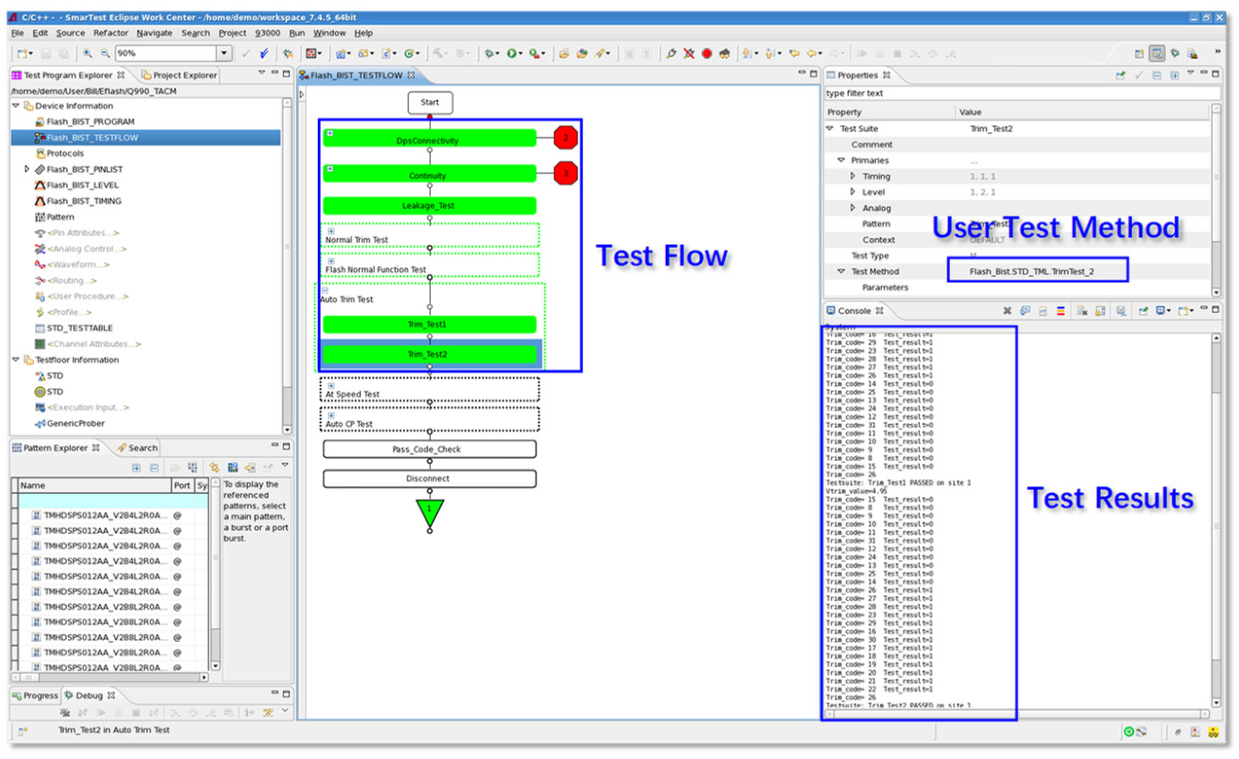
The test software is a test flow developed based on the 93 K SmarTest platform. The test stimulus signal is sent from the ATE, transmitted to the probe card through cables, and finally enters the test chip through a test pad. The test result is transmitted back to the test machine, and the final result is judged. The software environment of the 93 K test system is shown in
Figure 9, which consists of the CP flow and User Test Method.
The entire CP flow process is shown in
Figure 10. First, DC measurement is performed to check the connectivity of the test environment, and the leakage of each pin of the device under test is within a reasonable range:
- (1)
The Flash standard test process is followed, and the normal trim test of HV and the reference current is performed to ensure that the subsequent operation of Flash is correct and effective, reflecting real test results.
- (2)
The trim code is reloaded in the Flash register; then, the normal function verification of the Flash macro begins.
- (3)
After confirming that the sample function is normal, the auto-trimming test is carried out, and the result of the automatic trimming step is recorded as a trim code* to distinguish it from normal trimming results.
- (4)
If the result is as expected, the test is continued; otherwise, the original trim code needs to be reloaded into the register.
- (5)
The test ends.
The User Test Method is the user-defined test method that drives the hardware to complete the test by calling the function of the ATE test equipment. The detailed part of the program code used to improve the overall test efficiency is shown in
Appendix A.
5. Experimental Test Results
The analog circuit part verification mainly verifies the comparator’s response time and the comparator’s sampling time. The digital part of the simulation mainly verifies the relevant instruction set and the execution process of the entire auto-trimming step.
Through the actual test of the aforementioned verification chip, the total time of the auto-trimming step of the three-way signal VEG/VCG/VSL is about 0.23 s, accounting for 0.67% of the total test time. According to the data statistics of mass-produced products, in conventional auto-trimming with ATE measurement, the statistical value time of the three-way signal trimming ATE measured is about 2.94 s, accounting for 6.9% of the total test time. The main reasons why the embedded Flash takes too long to use the conventional Trimming method are as follows.
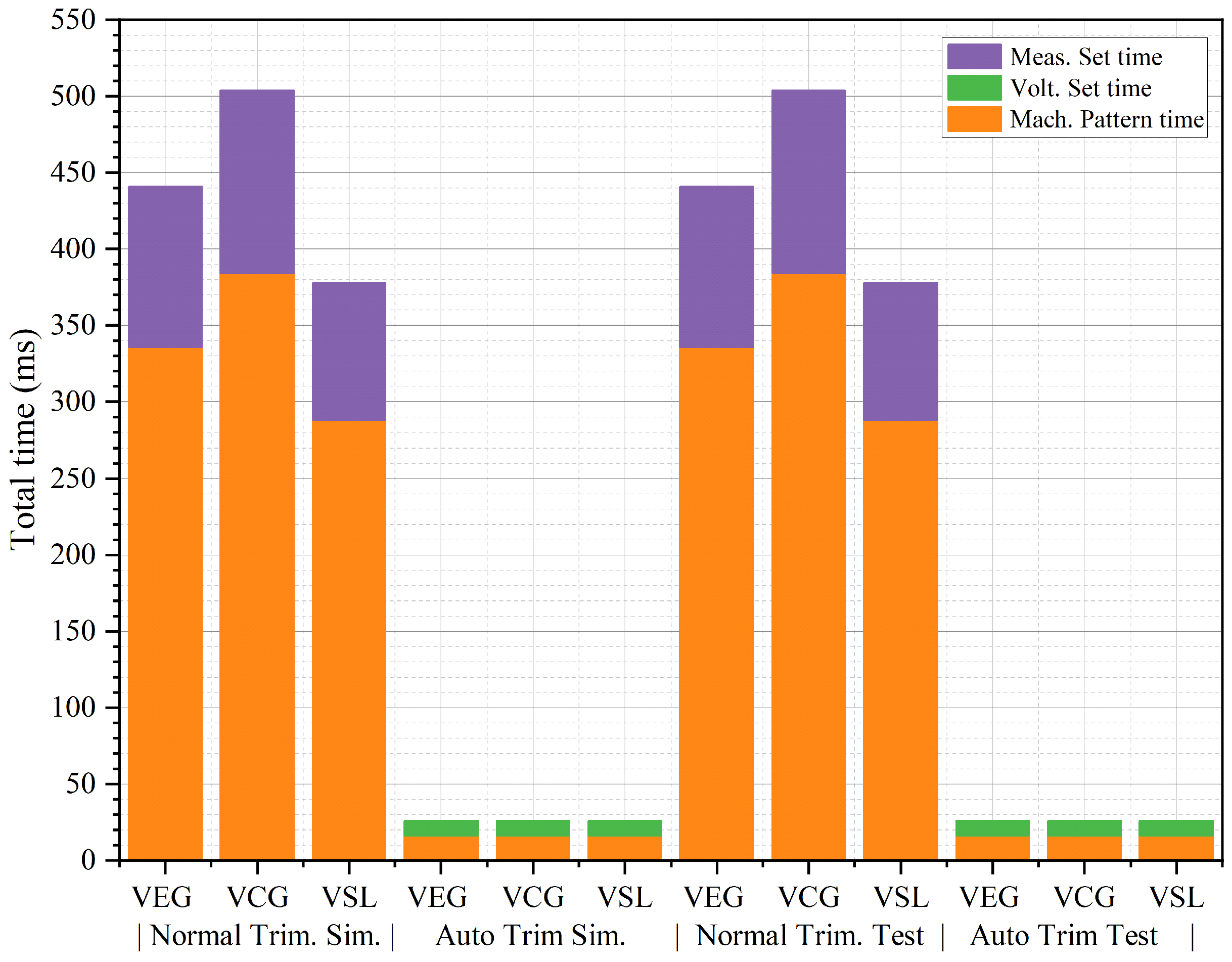
Setup time: Each time an individual interacts with an ATE machine, a certain setup time is required before and after calling the test pattern. Currently, the total waiting time is at least 6 ms. Therefore, during normal trimming, there are usually 8 to 10 interactions with the ATE. Each time a pattern is selected, 10 ms of setup time is required to wait for the pattern to stabilize. As shown in
Figure 11, the ATE machine measurement setup time, VEG/VCG/VSL, is about 400 ms in total, while the setup time in auto-trimming is only 48 ms.
Pattern execution time: When using ATE measurement resources, each measurement requires 10 ms of pattern execution time, while when using auto-trimming, only the voltage setup time is required, and voltage setup is only performed twice. Therefore, compared with normal trimming, auto-trimming saves at least about 1.5 s in this item.
Compared with the original BIST method, auto-trimming has a great advantage in both setup and pattern execution time when using ATE for trimming.
For the overall test time comparison, we refer the reader to the data in
Figure 12. In the simulation, the trimming time is reduced from 1.62 s to 0.2 s. In the actual measurement, the trimming time is reduced from 2.94 s to 0.23 s. In the simulation, the normal trimming test times and auto-trimming times are slightly lower than the actual time. The main error is that the waiting time in the simulation is an estimate of the ATE time.
From the ratio of trimming times to total test times, the ratio of using auto-trimming to normal trimming in the simulation is reduced from 4.2% to 0.5% (refer to
Figure 13a,b), and in actual measurements, it is reduced from 6.9% of normal trimming to 0.6% of auto-trimming (refer to
Figure 13c,d). A comparison of the area and total test time of the two BISTs is shown in
Table 1, and the test time is reduced by 6.35%.
A 60-chip test on a wafer was completed through auto-trimming. The test selected a comparator voltage divider resistor that was set to 0.25*VPP. After obtaining the trimming results, ATE measurement confirmation with the voltage divider resistor set to 0.4*VPP was performed. Simultaneously, the trimming of VEG was completed via the ATE method. The data distribution of the two measurement methods was compared according to the ratio of 0.4*VPP, which can satisfy the index requirement of 5 V ± 60 mV and actually reach 5 V ± 50 mV. The trimming result of the ATE measurement is within 5 V ± 1.6σ, and the result of auto-trimming is also within 5 V ± 1.6σ, as shown in
Figure 14. In addition, carrying out error analyses of the two measurement methods used on the 60-chip test, the error can be controlled within the industry’s standard requirement: equipment measurement error of 0.2% ± 6 mV. The actual error reaches 0.15% ± 7 mV, as shown in
Figure 15.
The newly added auto-trimming function of embedded Flash BIST was verified through the wafer verification and analysis of actual test results, indicating that the measurement efficiency of BIST for analog and high-voltage cases was significantly improved. In this field, architecture also has certain technological advancements.
6. Conclusions
In summary, the automated trimming of high-voltage and analog quantities can be carried out by adding and optimizing the digital part of the BIST circuit and analog circuits, thereby greatly reducing the test time of such test items. Subsequently, both new BIST circuits completed the verification chip design. After being fabricated using the 40 nm process, they successfully met the design requirements through the rewind test. Furthermore, an error analysis of the auto-trimming and ATE measurement trimming test results was also performed. The technical features described in this study comprise scientific research and industrial achievements based on a large number of engineering practices. In order to efficiently complete high-precision trimming, this technology reduces the ever-increasing demands on ATE resources and controls the cost of CP testing. This study provides a competitive BIST design scheme for the mass production CP testing of embedded Flash in mid-to-high-end automotive MCUs, providing a practical solution for the advancement of subsequent automotive MCU products. In the future, it can be applied to automotive MCU products in order to optimize mass production CP test times.
Author Contributions
Conceptualization, Q.L.; methodology, Q.L.; software, Q.L.; validation, Q.L.; formal analysis, Q.L.; investigation, Q.L.; resources, Q.L.; data curation, Q.L.; writing—original draft preparation, Q.L.; writing—review and editing, Q.L.; visualization, Q.L.; supervision, D.W.Z.; project administration, D.W.Z.; funding acquisition, D.W.Z. All authors have read and agreed to the published version of the manuscript.
Funding
This research received no external funding.
Data Availability Statement
The original contributions presented in this study are included in the article. Further inquiries can be directed to the corresponding author.
Conflicts of Interest
The authors declare no conflicts of interest.
Appendix A
The detailed part of the program code used to improve the overall test efficiency is as follows.
virtual void run()
{
//Add your test code here.
ERROR_MAP_TEST emap1(TM::TESTER_CYCLES);
SCAN_TEST_RESULT log1(TM::CYCLE_BASED_LOGGING);
GET_TESTSUITE_NAME(mTestName);
/* Setup the error map */
emap1.pin(scanPins1).setLocation(TM::RAM)
.setRecordingMode(TM::PF)
.setStartCycle(0);
/* Execute functional test */
FUNCTIONAL_TEST();
/* If functional test has passed, no further processing has to be done */
if(GET_FUNCTIONAL_RESULT()) {
return;
}
/* Retrieve the overall failures for this site */
log1.totalFailures(emap1.pin(scanPins1).getErrorCount());
log1.totalCyclesExecuted(emap1.getLastCycleExecuted());
/* Retrieve the failing cycles per pin for this site */
INT failsToUpload1 = emap1.pin(scanPins1).getErrorCount();
ARRAY_LL cycles1,cycles2,cycles3,cycles4;
emap1.pin(scanPins1).getFirstFailingCycles(0, failsToUpload1, cycles1);
log1.pin(scanPins1).failingCycles(cycles1);
/* Push the failures to datalog */
TESTSET().testsuite(mTestName).judgeAndLog_ScanTest(log1);
return;
} |
References
- Martirosyan, S.; Harutyunyan, G.; Shoukourian, S.; Zorian, Y. An efficient testing methodology for embedded flash memories. In Proceedings of the 2017 IEEE East-West Design & Test Symposium (EWDTS), Novi Sad, Serbia, 6–9 October 2017; pp. 1–4. [Google Scholar] [CrossRef]
- Liu, J.; Pan, F.; Zhou, D. The design of multilayer IC test board based on ATE. In Proceedings of the 2017 18th International Conference on Electronic Packaging Technology (ICEPT), Harbin, China, 16–19 August 2017; pp. 1552–1556. [Google Scholar] [CrossRef]
- Liu, Y.; Mukherjee, N.; Rajski, J.; Reddy, S.M.; Tyszer, J. Deterministic Stellar BIST for In-System Automotive Test. In Proceedings of the 2018 IEEE International Test Conference (ITC), Phoenix, AZ, USA, 28–30 October 2018; pp. 1–9. [Google Scholar] [CrossRef]
- Kaczmarek, B.B.; Mrugalski, G.; Mukherjee, N.; Rajski, J.; Rybak, Ł.; Tyszer, J. Test Sequence-Optimized BIST for Automotive Applications. In Proceedings of the 2020 IEEE European Test Symposium (ETS), Tallinn, Estonia, 25–29 May 2020; pp. 1–6. [Google Scholar] [CrossRef]
- Zhang, G.; Yuan, Y.; Liang, F. Low Cost Test Pattern Generation in Scan-Based BIST Schemes. Electronics 2019, 8, 314. [Google Scholar] [CrossRef]
- Tie, Z.; Ko, D.; Cheng, H.H. Embedded Ch based automatic testing environment for electronic products. In Proceedings of the 2012 IEEE/ASME 8th IEEE/ASME International Conference on Mechatronic and Embedded Systems and Applications, Suzhou, China, 8–10 July 2012; pp. 308–313. [Google Scholar] [CrossRef]
- Mao, J.; Long, Y.; Deng, Y.; Lu, Y.; Li, R.; Jiang, X. Key Technologies for Engineering Mass Production Testing of MCU Chips Based on ATE. China Integrated Circuit 2022, 31, 84–89. [Google Scholar]
- Bullag, R.F.; Ortega, R.C.; Bullag, S.B. Adaptive trimming test approach—The efficient way on trimming analog trimmed devices at wafer sort. In Proceedings of the 36th International Electronics Manufacturing Technology Conference, Johor, Malaysia, 4–6 November 2014; pp. 1–4. [Google Scholar] [CrossRef]
- Goh, S.H.; Chan, Y.H.; Lin, Z.; Lam, J. Concurrent built-in self-testing under the constraint of shared test resources and its test time reduction. Integration 2017, 59, 198–205. [Google Scholar] [CrossRef]
- Mittal, R.; Kawoosa, M.; Parekhji, R.A. Systematic approach for trim test time optimization: Case study on a multi-core RF SOC. In Proceedings of the 2014 International Test Conference, Seattle, WA, USA, 20–25 October 2014; pp. 1–9. [Google Scholar] [CrossRef]
- Suzuki, J.; Yamashita, J.; Suzuki, J.; Hanyu, M.; Ido, M.; Saito, T.; Nakashima, Y. A Cost-Effective High Accuracy Auto-Trimming System without Tester Constraint for Low-End Embedded Flash Memory. In Proceedings of the 2018 International SoC Design Conference (ISOCC), Daegu, Republic of Korea, 5–8 November 2018; pp. 48–49. [Google Scholar] [CrossRef]
| Disclaimer/Publisher’s Note: The statements, opinions and data contained in all publications are solely those of the individual author(s) and contributor(s) and not of MDPI and/or the editor(s). MDPI and/or the editor(s) disclaim responsibility for any injury to people or property resulting from any ideas, methods, instructions or products referred to in the content. |
© 2024 by the authors. Licensee MDPI, Basel, Switzerland. This article is an open access article distributed under the terms and conditions of the Creative Commons Attribution (CC BY) license (https://creativecommons.org/licenses/by/4.0/).


