Author Contributions
Conceptualization, data curation, formal analysis, investigation, methodology, validation, A.G.; writing—original draft, writing—review and editing, N.A.; supervision, funding acquisition, project administration, K.K.C. All authors read and agreed to the published version of the manuscript.
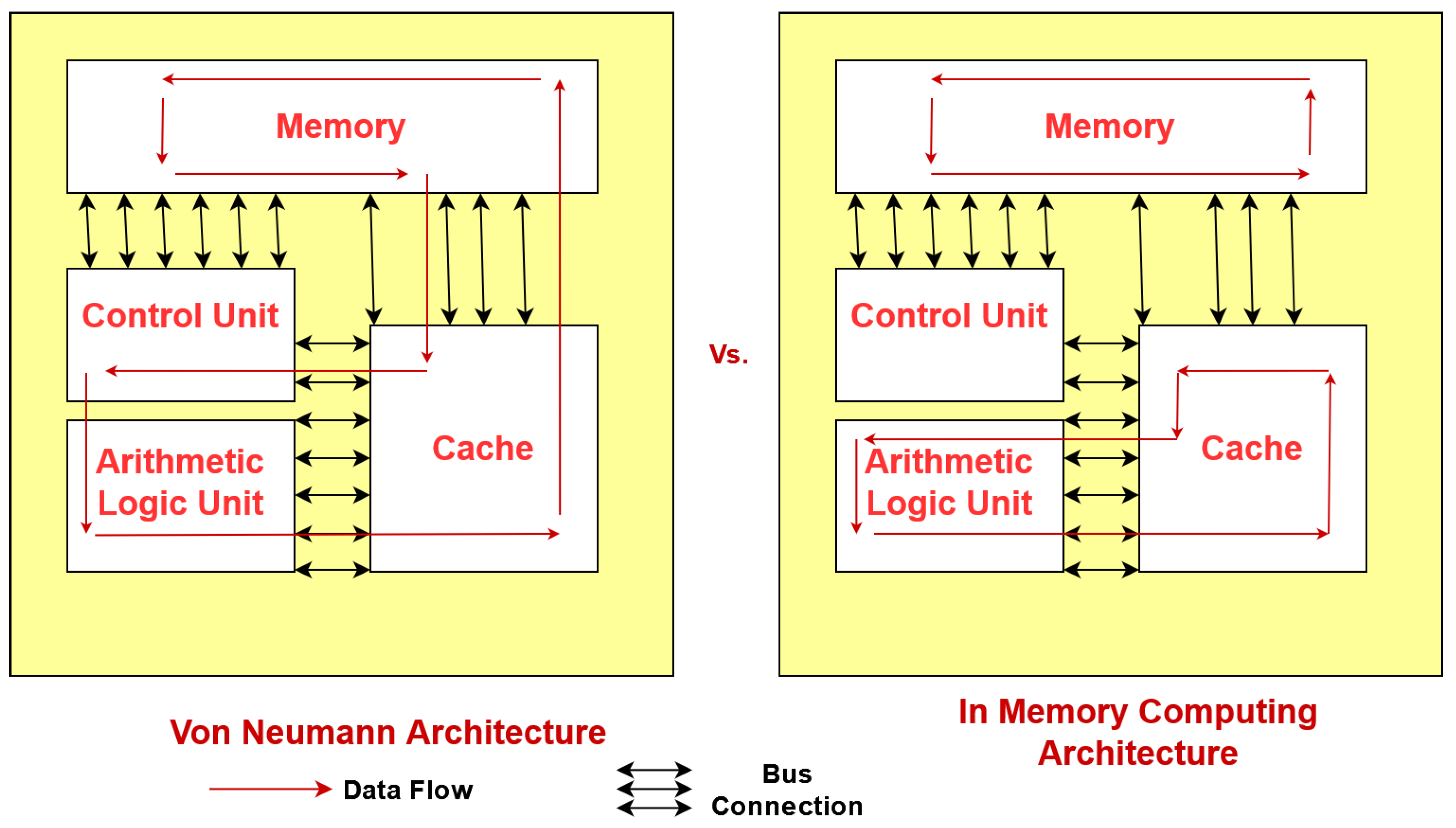
Figure 1.
Comparison between von Neumann and computing-in-memory(CIM) architecture.
Figure 1.
Comparison between von Neumann and computing-in-memory(CIM) architecture.
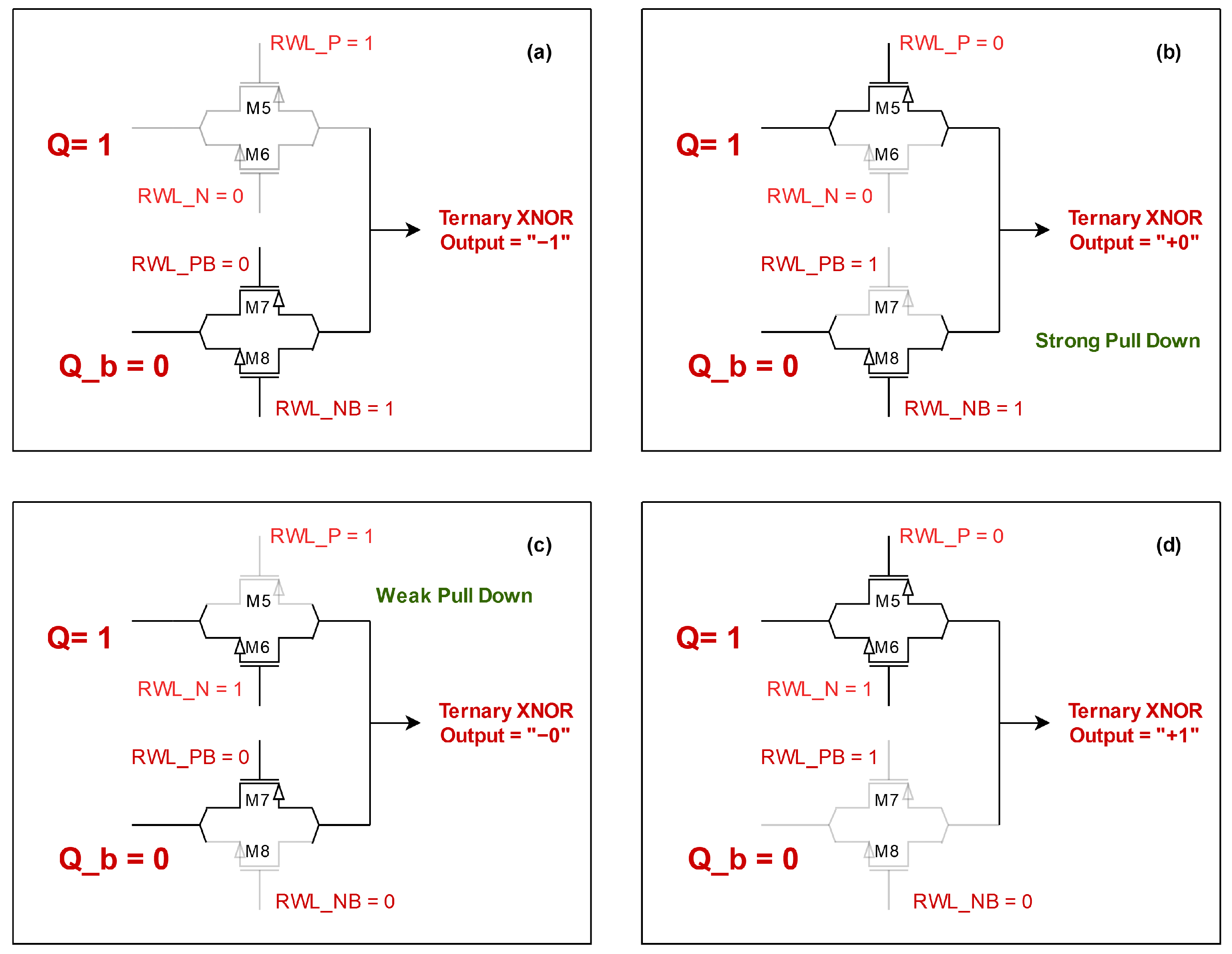
Figure 2.
Ternary XNOR operation with fixed weights and varying inputs. Subfigures (a–d) explains different XNOR inputs and desired outputs.
Figure 2.
Ternary XNOR operation with fixed weights and varying inputs. Subfigures (a–d) explains different XNOR inputs and desired outputs.
Figure 3.
P-Latch N-Access (PLNA) SRAM structure with XNOR logic.
Figure 3.
P-Latch N-Access (PLNA) SRAM structure with XNOR logic.
Figure 4.
Single-Ended (SE) SRAM structure with XNOR logic.
Figure 4.
Single-Ended (SE) SRAM structure with XNOR logic.
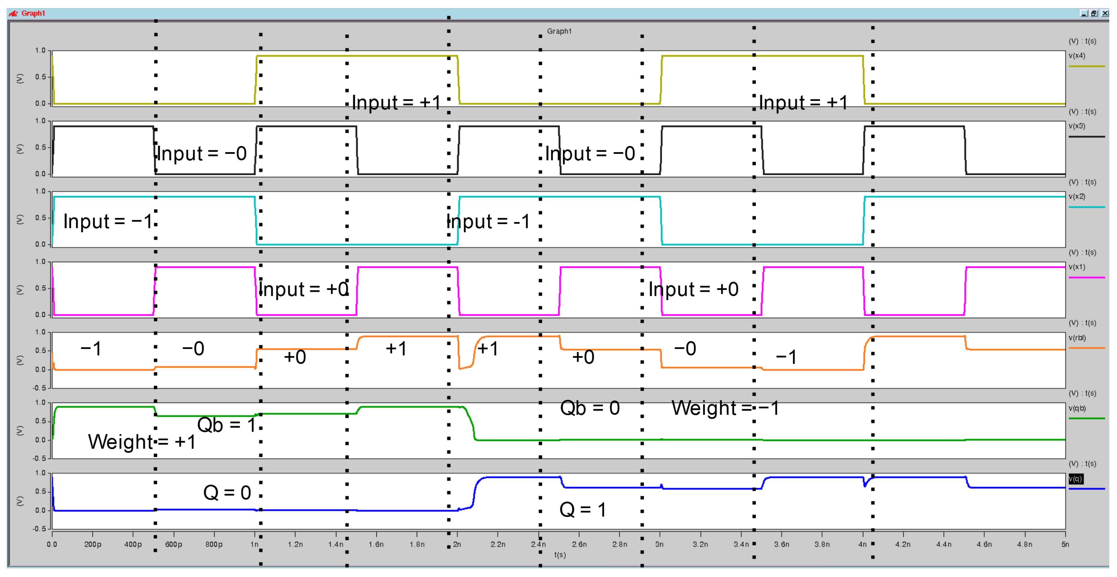
Figure 5.
Original SRAM waveform analysis of the proposed XNOR-SRAM CIM operation for ternary inputs. The input signals (+1, 0, −1, +0) are represented by yellow, black, cyan, and magenta lines, respectively. The ternary combination output (−1, 0, +1) is shown by the orange line. The complementary output Qb is indicated by the green line, while the primary output Q is represented by the blue line. The results illustrate correct ternary computation, highlighting the functionality of the XNOR pass transistor logic.
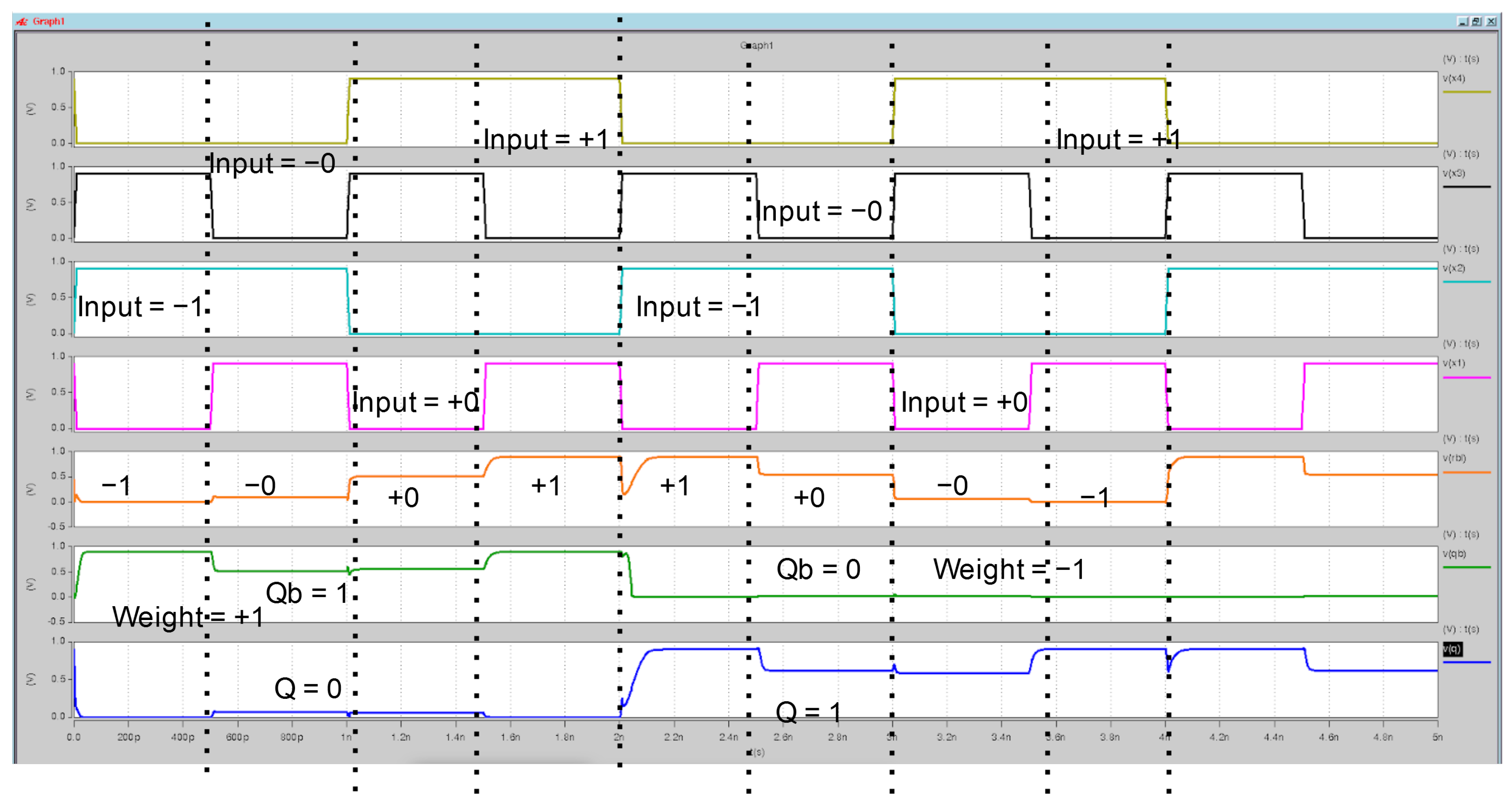
Figure 6.
PLNA SRAM waveform analysis of the proposed XNOR-SRAM CIM operation for ternary inputs. The input signals (+1, 0, −1, +0) are represented by yellow, black, cyan, and magenta lines, respectively. The ternary combination output (−1, 0, +1) is shown by the orange line. The complementary output Qb is indicated by the green line, while the primary output Q is represented by the blue line. The results illustrate correct ternary computation, highlighting the functionality of the XNOR pass transistor logic.
Figure 7.
SE SRAM waveform analysis of the proposed XNOR-SRAM CIM operation for ternary inputs. The input signals (+1, 0, −1, +0) are represented by yellow, black, cyan, and magenta lines, respectively. The ternary combination output (−1, 0, +1) is shown by the orange line. The complementary output Qb is indicated by the green line, while the primary output Q is represented by the blue line. The results illustrate correct ternary computation, highlighting the functionality of the XNOR pass transistor logic.
Table 1.
Logic Map for the Product Between the Input and the Weight.
Table 1.
Logic Map for the Product Between the Input and the Weight.
| Input Value | Inputs | Weights | Weights Value | Outputs RBL |
|---|
| RWL_P | RWL_N | RWL_PB | RWL_NB | Q | Q_b |
|---|
| −1 | 1 | 0 | 0 | 1 | 1 | 0 | +1 | −1 |
| +0 | 0 | 0 | 1 | 1 | 1 | 0 | +1 | 0 |
| −0 | 1 | 1 | 0 | 0 | 1 | 0 | +1 | 0 |
| +1 | 0 | 1 | 1 | 0 | 1 | 0 | +1 | 1 |
| −1 | 1 | 0 | 0 | 1 | 0 | 1 | −1 | 1 |
| +0 | 0 | 0 | 1 | 1 | 0 | 1 | −1 | 0 |
| −0 | 1 | 1 | 0 | 0 | 0 | 1 | −1 | 0 |
| +1 | 0 | 1 | 1 | 0 | 0 | 1 | −1 | −1 |
Table 2.
Transistor Sizing for FinFET in PLNA 8T SRAM Cell.
Table 2.
Transistor Sizing for FinFET in PLNA 8T SRAM Cell.
| Number | Transistor | Number of FINS |
|---|
| 1 | M1 | 1 |
| 2 | M2 | 1 |
| 3 | M3 | 2 |
| 4 | M4 | 2 |
| 5 | M5 | 1 |
| 6 | M6 | 4 |
| 7 | M7 | 1 |
| 8 | M8 | 4 |
Table 3.
Transistor Sizing for FinFET in SE 8T SRAM Cell.
Table 3.
Transistor Sizing for FinFET in SE 8T SRAM Cell.
| Number | Transistor | Number of FINS |
|---|
| 1 | M1 | 1 |
| 2 | M2 | 1 |
| 3 | M3 | 2 |
| 4 | M4 | 4 |
| 5 | M5 | 1 |
| 6 | M6 | 4 |
| 7 | M7 | 1 |
| 8 | M8 | 4 |
Table 4.
Comparison of Power Consumption for Different Weights, Inputs, and RBL States across Original, 7 nm FinFET PLNA, and 7 nm FinFET SE Configurations.
Table 4.
Comparison of Power Consumption for Different Weights, Inputs, and RBL States across Original, 7 nm FinFET PLNA, and 7 nm FinFET SE Configurations.
| Weight | Input | RBL | Power (W) |
|---|
| Original [12] | FinFET 7 nm PLNA | FinFET 7 nm SE |
|---|
| +1 (Q=H, Qb=L) | −1 | Discharge | 2.579 | 1.179 | 0.874 |
| +1 (Q=H, Qb=L) | +0 | Stable | 189.86 | 70.867 | 83.384 |
| +1 (Q=H, Qb=L) | −0 | Stable | 118.21 | 63.74 | 41.462 |
| +1 (Q=H, Qb=L) | +1 | Charge | 23.3 | 4.858 | 5.798 |
| −1 (Q=L, Qb=H) | −1 | Charge | 1.8853 | 1.081 | 0.76809 |
| −1 (Q=L, Qb=H) | +0 | Stable | 119.53 | 64.34 | 42.07 |
| −1 (Q=L, Qb=H) | −0 | Stable | 185.6 | 69.2 | 78.85 |
| −1 (Q=L, Qb=H) | +1 | Discharge | 6.611 | 4.11 | 2.2427 |
Table 5.
Overall Power Comparison of FinFET Designs.
Table 5.
Overall Power Comparison of FinFET Designs.
| Design | Total Power (W) | Difference (W) | Percentage Reduction (%) |
|---|
| FINFET Original [12] | 81.401 | – | – |
| FINFET PLNA | 35.093 | −46.308 | 56.90% |
| FINFET SE | 32.2123 | −49.1887 | 60.42% |
Table 6.
Total Delay (8 Rows and Single Column).
Table 6.
Total Delay (8 Rows and Single Column).
| Design | Total Delay |
|---|
| Original [12] | 1.009 ns |
| PLNA | 0.713 ns |
| SE | 0.501 ns |
Table 7.
Delay Comparison for Different Operations.
Table 7.
Delay Comparison for Different Operations.
| Operation | Original (pS) [12] | SE (pS) | PLNA (pS) |
|---|
| +1 | 23.77 | 0.5073 | 1.124 |
| 20.652 | 0.29143 | 4.9496 |
| +1 × +1 | 20.57 | 0.3612 | 2.052 |
| +1 | 21.22 | 0.5463 | 1.1154 |


