Review

Design Strategies of Integrated Metal-Oxide Semiconductor-Based Resistive Sensor Systems for Ammonia Detection

1
Information Science Academy of China Electronics Technology Group Corporation, Beijing 100042, China
2
National Key Laboratory of Integrated Circuits and Microsystems, Beijing 100042, China
3
School of Mechanical Engineering, Shijiazhuang Tiedao University, Shijiazhuang 050043, China
*
Author to whom correspondence should be addressed.
Electronics 2024, 13(23), 4800; https://doi.org/10.3390/electronics13234800
Submission received: 7 October 2024 / Revised: 21 November 2024 / Accepted: 29 November 2024 / Published: 5 December 2024
(This article belongs to the Special Issue RF/Microwave Circuit Design and Its Application)

Abstract

:
Chemical production activities cause large amounts of ammonia to evaporate into the atmosphere, degrading air quality and even endangering public health, so monitoring ammonia in real time is significant. Traditional detection techniques, including spectrometers, chromatography, and pumping methods, are characterized by high costs, complex operation, significant delays, and limited compatibility, which obstructs the immediate identification of ammonia and the timely provision of information. Due to their distinct benefits such as compact size, affordability, quick response time, and lack of need for manual operation, resistive ammonia sensors hold significant promise for the real-time tracking of ammonia emissions in chemical manufacturing processes. In recent years, sensors utilizing metal-oxide semiconductor (MOS) nanomaterials have become a popular area of research due to their high sensitivity, strong stability, and acceptable response and recovery times. However, the interface circuits of existing MOS gas sensors mainly focus on sensor configuration and data acquisition. These interface circuits lack the functions of array timing control and data processing; gas detection and identification cannot be realized directly by them, which reduces the system integration and increases the application complexity. This paper begins by examining key design strategies for MOS-based resistive sensors aimed at enhancing ammonia sensing capabilities, offering researchers a foundation for their work in creating high-performance ammonia sensors. Based on this, a complete measuring system and a programmable interface circuit for an MOS gas sensor are introduced, which can integrate sensor configuration, signal acquisition, data processing, and output of recognition results. Finally, the current challenges and future opportunities of MOS-based resistive ammonia sensor systems are presented. The purpose of this review is to offer researchers suggestions for creating high-performance MOS-based resistive ammonia sensor systems and to promote the use of these sensors in upcoming chemical manufacturing processes.

1. Introduction

Ammonia is a colorless, toxic gas that dissolves in water and has a strong, sharp smell [1]. Ammonia plays a vital role in a multitude of chemical manufacturing processes, serving as a key ingredient in the creation of nitric acid. Its versatility extends to light industry, where it fuels the production of chemical fertilizers, pharmaceuticals, pesticides, refrigerants, synthetic fibers, and much more [2,3,4,5]. However, these production activities cause large amounts of ammonia to evaporate into the atmosphere [6]. Ammonia in the atmosphere plays a crucial role in forming tiny particles that can harm air quality and pose serious risks to our respiratory health [7]. Inhaling a specified quantity of ammonia can induce a range of toxic symptoms, posing significant risks to human health and life [8]. Therefore, real-time monitoring of ammonia gas is of great significance to ensure the safety of chemical production activities and the living environment.
The traditional techniques used to keep an eye on ammonia emissions encompass a variety of tools such as spectrometers, chromatography, gas detection tubes, and pumping systems [9,10,11,12]. Nonetheless, these approaches are limited by their high cost, complex operation, significant delays, and limited compatibility, which obstructs the immediate identification of ammonia and the timely provision of information [13,14,15]. In addition, these technologies are highly dependent on manual operation and cannot meet the requirements of modern chemical production [16,17,18]. Unlike the detection methods previously discussed, gas sensing technologies excel with their unique benefits: they are compact, budget-friendly, quick to react, and require no hands-on operation. These qualities open up exciting possibilities for the real-time tracking of ammonia emissions in today’s chemical manufacturing landscape [19,20,21]. Among them, resistive gas sensing technology stands out because it is easy to integrate [22,23]. The swift advancement of communication and semiconductor technologies has enabled the seamless integration of resistive gas sensors with communication chips, drivers, and software algorithms. This integration has resulted in the creation of multi-component circuits that are capable of exchanging and storing information, along with performing various other functions [24,25].
The gas-sensitive material is fundamental to the operation of resistive ammonia sensors, playing a crucial role in their functionality [9,10,26]. In recent years, the spotlight has shone brightly on sensors crafted from metal-oxide semiconductor (MOS) nanomaterials. Their remarkable sensitivity, impressive stability, and swift response and recovery times have made them a hot topic of research and innovation [24,27,28]. A diverse range of metal-oxide semiconductor (MOS) materials, including zinc oxide (ZnO), tin dioxide (SnO2), and tungsten trioxide (WO3), has been extensively employed in the development of gas sensors for ammonia detection [29,30,31]. The characteristics of these materials are presented in Table 1. Furthermore, to enhance the ammonia sensing capabilities of metal-oxide semiconductor (MOS) materials, researchers are actively engaged in the development of novel methodologies. Among them, single-element decorated and composite MOS nanomaterials have been proved to effectively improve the ammonia sensing performance of single nanomaterials [32,33,34,35]. Doping alters not just the internal electronic properties of the grain but also its structure [36,37]. Doping significantly improves the characteristics of gas-sensitive materials by altering the grain size, affecting the concentration of internal defects or charge carriers, and augmenting the pathways for oxygen vacancies [38,39]. The composite MOS nanomaterials can make full use of the synergistic effect between the components to improve the ammonia sensing performance [40,41,42]. In addition, a complete gas sensor must be an integral part of gas-sensitive material and signal conversion circuit in order to meet the practical requirements of application environments. PCBs have obvious problems of high power consumption and large area, which makes them gradually unable to meet the development needs of miniaturization and integration of gas sensors. The microelectronic technology provides a great help to the development of Application Specific Integrated Circuit (ASIC) chips with small area, high integration, and low power consumption.
To date, intensive work has been published on MOS nanomaterials, including single nanomaterials, single-element decorated nanomaterials, and composite nanomaterials, providing development processes on resistive ammonia sensors, and, as shown in Figure 1, this research is receiving increasing attention based on the trend of publication numbers in recent years [43,44,45]. Design strategies for these sensors based on MOS nanomaterials are essential for their widespread application in chemical production activities. Motivated by the pressing need for innovation, this study conducts a focused examination of the most recent developments and noteworthy initiatives in the creation of metal-oxide semiconductor (MOS)-based resistive sensors for ammonia detection [46,47,48]. This document emphasizes key strategies for enhancing ammonia sensing performance, presents notable examples within this field, and discusses the most recent design frameworks for MOS nanomaterials and interface circuits utilized in ammonia sensors. This review highlights recent advancements in MOS-based resistive ammonia sensors, focusing on improvements in sensing mechanisms, sensor design, and interface circuit integration. By examining these aspects, this review aims to provide insights that guide researchers in developing high-performance MOS ammonia sensors and promoting their application in future chemical production and environmental monitoring.

2. Gas Sensing Mechanism of MOS-Based Resistive Sensors

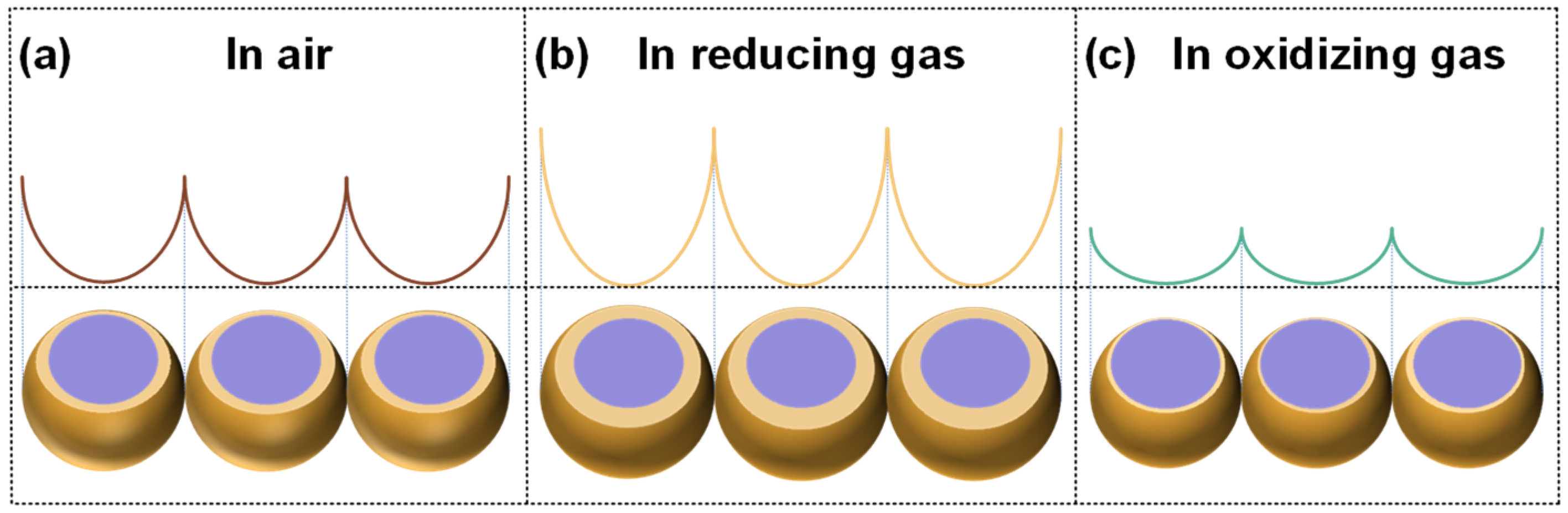
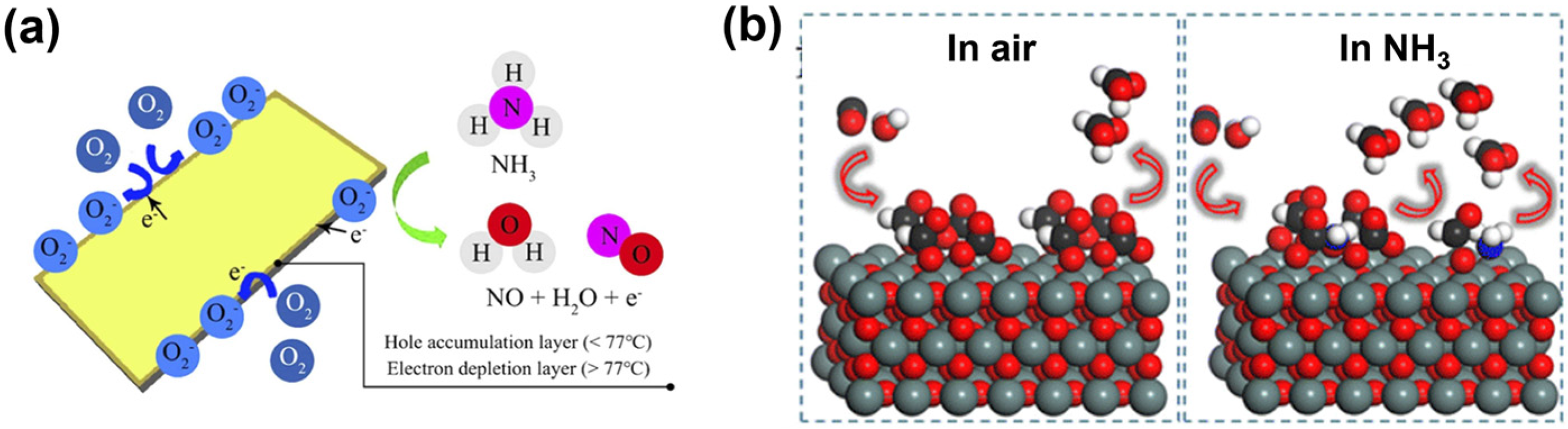
2.1. Resistive Sensor Detection Mechanisms for n-Type Oxide Films

In terms of specific surface area increase, by controlling the nanostructure of the MOS material (e.g., nanowires, nanoparticles, or porous structure), the specific surface area of the material can be significantly increased, which in turn increases the chances of the gas molecules to come into contact with the surface of the material. This helps to increase the gas adsorption capacity of the material and thus enhances the sensing sensitivity. In terms of surface defects and oxygen vacancies, the surface defects (e.g., oxygen vacancies) of MOS materials can act as active sites to enhance the adsorption and reaction of gas molecules by the materials. The presence of oxygen vacancies improves the sensitivity of the material to reducing gases and can accelerate the reaction of gas molecules with the surface active sites. In precious metal modification, Schottky junctions can be formed by modifying precious metals (e.g., gold, silver, palladium) on the surface of the MOS material to improve the charge transfer efficiency. Precious metal modification not only improves the selectivity of the sensor but also enhances the response speed and sensitivity. In terms of operating temperature optimization, MOS sensors usually show better performance at high temperatures. Increasing the operating temperature accelerates the reaction rate of gas molecules with the material surface, thus improving the response time and sensitivity of the sensor [49].
The way metal oxides detect changes is primarily linked to their resistance shifting, which occurs through surface interactions with oxygen species that have already settled on them (O2−, O, O2) and various gas molecules. Upon exposure to atmospheric air, metal oxides undergo a process in which chemisorbed oxygen ions are generated through the extraction of free electrons from the conduction band of the metal oxides. This results in a reduction of electron concentration at the surface, leading to the formation of an electron depletion layer. Hence, the resistance of metal oxides increases [50]. Various forms may be observed depending on the operating temperature, with the predominant species being O2 at temperatures below 100 °C (Equation (1)). When the operating temperature is elevated within the range of 100 °C to 300 °C, the O2 ions will acquire electrons, resulting in their conversion to O ions (Equation (2)). The O ions can be transformed into O2− ions when subjected to elevated temperatures exceeding 300 °C (Equation (3)).
O 2 ( ads ) + e O 2 ( ads )   ( < 100   ° C )
O 2 ( ads ) + e 2 O 2 ( ads )   ( 100 ~ 300   ° C )
O ( ads ) + e O ( ads ) 2   ( > 300   ° C )
Upon exposure to the target gases, gas molecules may be adsorbed onto the surface of metal oxides or may engage in reactions with the chemisorbed oxygen ions present on that surface. Using the n-type MOS as an example, when it comes into contact with air, oxygen ions are chemically adsorbed by extracting free electrons from the conduction band of the n-type MOS. This leads to a decrease in electron concentration at the surface, resulting in the upward bending of the surface energy bands and the formation of an electron depletion layer at the surface (Figure 2a). When the n-type MOS interacts with reducing gas molecules, these gas molecules engage with the oxygen species that are adsorbed, resulting in the release of electrons onto the surface of the n-type MOS (Figure 2b). Consequently, the electron concentration at the surface increases, which diminishes the degree of upward bending of the surface energy bands and narrows the width of the surface electron depletion layer. Consequently, the barrier height at the grain boundaries of the n-type MOS diminishes, leading to a reduction in the overall resistance of the MOS. When the n-type MOS encounters oxidizing gas molecules, a fascinating dance begins. These gas molecules engage with the oxygen species clinging to the surface, or they may settle directly onto the n-type MOS, pulling electrons away from the surface in a captivating exchange (Figure 2c). This phenomenon results in a diminished electron concentration at the surface of the n-type metal-oxide semiconductor (MOS), which in turn causes a more pronounced upward curvature of the surface energy bands and an expansion of the surface depletion region. Consequently, the barrier height at the grain boundaries of the MOS is elevated, leading to an increase in the overall resistance of the MOS structure.
In environments with high humidity, proton transfer processes (Grotthuss mechanism) may occur during surface adsorption. Intermediate species (e.g., NH4+ and OH) may be generated when ammonia molecules react with the surface active sites of the material. These species diffuse on the surface by proton hopping, thus accelerating the kinetic process of the surface reaction. The Grotthuss mechanism significantly affects the response time and recovery time of the sensor through the surface hydrogen bonding network. According to the HSAB theory, ammonia molecules act as Lewis bases and interact with Lewis acidic sites on metal oxide surfaces. Hard acidic sites (e.g., oxygen vacancies and surface oxygen ions) tend to strongly adsorb ammonia, while soft acidic sites (e.g., noble metal-modified sites) further enhance the sensitivity and selectivity by enhancing the electron transfer efficiency. The acid–base interaction mechanism provides theoretical support for the selective adsorption of ammonia molecules at surface active sites.

2.2. Resistive Sensor Detection Mechanisms for p-Type Oxide Films

P-type metal-oxide semiconductor (MOS) materials (e.g., nickel oxide (NiO), copper oxide (CuO)) exhibit a different sensing mechanism in ammonia detection than n-type materials. When an ammonia molecule comes in contact with the surface of a p-type MOS material, the following reaction process occurs, leading to a change in the material resistance. Adsorption of ammonia molecules and electron acceptor behavior: p-type MOS materials are usually rich in holes, and, when ammonia molecules (as reducing gases) are adsorbed onto the surface of the material, they react with the oxygen molecules on the surface of the material, leading to electron transfer between the surface oxygen ions and the ammonia molecules. The ammonia molecules will reduce the oxygen molecules adsorbed on the surface, releasing the electrons. Since holes are the main carriers in p-type materials, the introduction of electrons leads to a decrease in the concentration of holes, thus increasing the resistance of the material. Reaction Mechanism of Resistance Change: The adsorption of ammonia molecules onto the surface of the p-type material reacts with the surface oxygen, reducing the concentration of holes available in the material. This decrease in hole concentration directly leads to a decrease in the conductance of the p-type material, i.e., an increase in the resistance of the material. This increase in resistance contrasts with the n-type MOS materials (which typically have a decreased resistance in the presence of ammonia). p-type vs. n-type Material Differences on Sensing Systems: The increased resistance of p-type materials in ammonia environments makes them uniquely suited for selective detection. For mixed gas environments, p-type and n-type materials can be used in combination to build differential sensors to enhance the selectivity and sensitivity of the sensor. p-type MOS materials’ properties for ammonia detection make them suitable for specific application scenarios, such as detection tasks that require high selectivity and specific environmental adaptability.

2.3. Material Characteristics of Resistive Sensors

The physicochemical properties of the material, such as surface structure, porosity, electrical conductivity, and chemical stability, directly affect its electrochemical properties in gas sensors. Metal-oxide semiconductor (MOS) nanomaterials can provide more adsorption sites due to their large specific surface area and high surface activity, thus improving the responsiveness to gas molecules, and their electrochemical properties such as electron transfer efficiency, response time and, selectivity [51]. The choice of material design determines the final electrical properties of the sensor and influences the design requirements of the circuit system. For example, designing MOS materials with specific defect structures can enhance the sensitivity of the sensor, which means that the circuit part needs to be designed with a high-resolution signal reading system to accurately capture changes in low gas concentrations. At the same time, the stability of the material affects the need for noise suppression and data stability in the circuit design. Therefore, by optimizing the material properties, a more stable and sensitive signal can be provided to the sensing system, which leads to an optimized design of the circuit and provides a reliable input for subsequent signal processing [52].

3. Design Strategies for MOS-Based Resistive Sensors

3.1. Single Nanomaterial

The crystal morphology and structure of MOSs are of paramount importance for their gas sensing properties, given the sensitive nature of the material [53]. Tungsten trioxide (WO3) is a typical N-type semiconductor with an anisotropic layered crystalline structure, which has the advantages of excellent physical and chemical properties, non-toxicity, and good stability. Jian et al. synthesized the urchin-like WO3 (Figure 3a) by one-step hydrothermal method [54]. The urchin-like structure of WO3 is characterized by needle-like nanorods, which create a distinctive hierarchical arrangement that enhances the specific surface area of WO3 and offers an increased number of active sites for gas-sensitive reactions. When exposed to 30 ppm ammonia, the nanomaterial demonstrated a significant gas response, notable selectivity, and commendable repeatability and stability. Wang et al. synthesized closely packed WO3 microspheres with oxygen vacancy (Figure 3b) by a two-step hydrothermal method [55]. The introduction of oxygen vacancy greatly improved the electron injection efficiency of ammonia into the conduction band by changing the band structure and constitutive impedance of WO3. The synthesized nanomaterial demonstrated a high selectivity for ammonia, exhibiting a response intensity that was 2.6 times greater than that of commercially available WO3. Xu et al. developed a novel hierarchical WO3 nanomaterial characterized by a seawave-like morphology (Figure 3c), which is comprised of worm-like WO3 nanowires [56]. The worm-like nanowires facilitated a substantial number of ammonia diffusion pathways and offered an extensive surface area for ammonia-sensitive reactions. Additionally, they enhanced the directional transport of electrons, thereby augmenting the gas sensing characteristics of WO3. In addition to WO3, other MOS nanomaterials with excellent properties have also been extensively developed by researchers for ammonia sensing. Vasiliev et al. synthesized two-dimensional (2D) SnO2 nanosheets by surfactant-assisted one-pot solution synthesis [27]. The nanosheets had the characteristics of high specific surface area and increased surface acidity, providing a high sensor signal for ammonia in dry air. Wang et al. synthesized durian-like NiO nanomaterials (Figure 3d) using nickel hydroxide as precursors [57]. The durian-like NiO structure modified with nanocones had a large active surface area and could adsorb a large number of ammonia molecules. Each ammonia molecule with lone pair electrons was an electron donor and easily provided electrons, resulting in improved gas-sensitive properties of the nanomaterials. Zhao et al. prepared Cu2O concave octahedrons (Figure 3e), dodecahedrons, and cubes by a simple hydrothermal reaction [58]. The Cu2O concave octahedrons owned an exposed high-index facet {511}, which had a higher ammonia adsorption energy and transfers more electrons when interacting with the N atom in ammonia, resulting in a significantly improved gas sensing performance to ammonia. Wei et al. fabricated Co3O4 hexagonal platelets (Figure 3f) with high energy facets (112) by a simple method [59]. The vibrant energy aspect boasted a spacious active site, a compact bond length, and a robust adsorption energy between ammonia and the sensing surface. This combination rendered the Co3O4 nanomaterials exceptional in their ability to detect ammonia gas.
In addition, researchers are working on the optimization of the nanomaterials’ preparation process. Alwan et al. prepared SnO2 on the photoelectrochemical etched substrate with quick response and recovery times by optimizing the deposition temperatures during the spray pyrolysis technique [60]. Similarly, Serkan optimized the process temperature and time for WO3 nanoflake formation on a substrate [61]. Ravindra reported an optimized chemical vapor deposition (CVD) synthesis method for an ammonia sensor based on Cu2O, making the sensor more repeatable, stable, and reproducible [62]. Gun developed an innovative ammonia gas sensor utilizing n-CuO, employing three-dimensional (3D) printing through the fused deposition modeling technique in conjunction with a sintering process, as illustrated in Figure 4a [63]. The innovative design has opened up a world of active pore sites, boosting gas adsorption and sensitivity at room temperature. In a remarkable feat, Yeh and colleagues crafted a TiO2 gas sensor using cutting-edge 3D through-silicon via technology (TSV) combined with atomic layer deposition (ALD). A schematic image of the fabrication process for the 3D TSV-structured TiO2 gas sensor is shown in Figure 4b [64]. The TiO2 thin film was a p-type semiconductor with an anatase phase, leading to good stability, reproducibility, and selectivity.
In conclusion, the research on single nanomaterials in the ammonia sensing field is mainly on MOSs, focusing on structural sensitization of nanomaterials. By changing crystal morphology and structure, the specific surface area is increased to promote the exposure of the active site, to improve the ammonia sensing properties. However, the method of optimizing single materials usually has certain limitations, and the reasonable introduction of other materials can further improve the ammonia sensing properties from the aspect of electronic and chemical sensitization.

3.2. Single-Element Decorated Nanomaterials

Enhancing the ammonia sensing capabilities of individual nanomaterials can be effectively achieved through the art of single-element decorating. Among the various embellishments, noble metals take center stage, primarily serving as catalysts. They work their magic by lowering the activation energy required for ammonia molecules to break apart and react, ultimately boosting the efficiency of gas detection [65,66]. Gold has garnered significant attention for its remarkable qualities, including exceptional stability, impressive catalytic prowess, and a versatile operating temperature range [67,68]. Yu et al. presented the development of dumbbell-shaped Au-Fe3O4 nanomaterials intended for use as ammonia sensors. The study demonstrated that the particle sizes of both gold (Au) and iron oxide (Fe3O4) could be adjusted across a broad spectrum [61]. The remarkable ability of Au-Fe3O4 to detect ammonia stems from the Schottky junction that emerges at the boundary between gold and iron oxide, coupled with the unique surface plasmon effects of gold. In an exciting development, Han and colleagues crafted stunning Au-adorned GaN nanoflowers using a hydrothermal technique, which involved a high-temperature nitridation and an in situ reduction process [69]. The schematic diagram of the ammonia sensing mechanism and energy band structure of Au-GaN nanoflowers are shown in Figure 5a. Similarly, the improved sensing performance was attributed to the co-action of electronic and chemical sensitization. Ag has also been proven to be an efficient co-catalyst that can improve ammonia sensing performance. Liu and colleagues crafted an innovative ammonia sensor using Bi2MoO6, enhanced with the addition of silver. This remarkable device is capable of detecting ammonia concentrations as low as parts per billion, all while operating at room temperature [70]. In Figure 5b, we show an interesting schematic that illustrates the ammonia sensing mechanism alongside the intricate energy band structure. Thanks to the spillover effect of silver nanoparticles and the metal–semiconductor junction created between silver and Bi2MoO6, the ammonia sensing capabilities have been significantly amplified. Zheng et al. prepared the porous Ag-ZnO nanostructured film via physical vapor deposition (PVD) and thermal annealing [71]. To enhance the peak response and detection speed of ammonia, one can boost the effective surface area and enlarge the macropores in nanostructured films. In a fascinating study, Qiu and colleagues took a classic approach by applying a Ru catalyst onto the surface of WO3 nanosheets through a traditional impregnation method. They then transformed this innovative combination into an ammonia sensor using the art of screen-printing technology [72]. As shown in Figure 5c, due to the catalytic activity of Ru, the formation of NO as an intermediate product was inhibited, significantly improving the response to ammonia. Similarly, using the catalytic activity of Pt films, Chen et al. developed an ammonia gas sensor based on a combination of Pt and NiO [40]. The sensor showcased remarkable capabilities, particularly its astonishingly low detection threshold of just 10 parts per billion of ammonia in the air. Dai and colleagues crafted a singular Pd-WO3·xH2O microwire to serve as an ammonia sensor, employing a cutting-edge femtosecond laser direct-writing technique for precision [73]. The methodology demonstrated the capability to synthesize a range of sensing nanomaterials accurately, flexibly, and graphically, thereby offering a viable approach for the development of miniaturized ammonia sensors.
In addition to noble metals, other metals can also be used to improve the ammonia sensing properties of nanomaterials. Garshev et al. demonstrated formation of Cr(VI) lattice defects on the surface of Cr-doped SnO2, leading to acidity improvement [74]. Additionally, substitutional Cr(III) defects formation caused a decrease in free electron concentration in the conduction band, leading to an increase in electrical resistivity. Therefore, Cr doped with MOS could inhibit the sensitivity of NO2 and improve the response to ammonia. Using this improved sensing mechanism, Sun et al. prepared Cr-doped In2O3 with large specific surface areas [75]. As shown in Figure 6a, the nanomaterials had an extremely fast response speed (1 s) for 1 ppm ammonia sensing. Similarly, Li et al. introduced Ni to decorate In2O3 to increase the reactive oxygen species and surface acidity significantly, thus improving the ammonia sensing properties [76]. Nataliya et al. doped Sn in Ga2O3 to improve the conductivity of nanomaterials, leading to a sharp increase in sensor signal [77]. Varudkar et al. fabricated Al-doped ZnO nanoparticles by a simple co-precipitation technique [78]. Through Al doping, the morphology of the nanomaterials changed from a hexagonal crystalline phase of ZnO structure to a spherical crystal phase of Al-ZnO, leading to good response and recovery times to ammonia. In a similar vein, Yao infused Sb into WO3, altering the valency of tungsten and sparking a fascinating partial transformation of the crystal structure from its orthorhombic form to a sleek hexagonal shape [79]. The alteration of W valency enhanced the ammonia detection capabilities of Sb-WO3, particularly at temperatures close to room temperature. The intricacies of the charge transfer process and the mechanism behind ammonia vapor sensing are illustrated in Figure 6b. In addition, there are some reports of non-metallic element decoration to improve the ammonia sensing properties. Take, for instance, carbon-doped SnO2, which boasts remarkable features like resistance to interference, impressive selectivity, and an incredibly low detection threshold for ammonia, all while operating at room temperature [80]. These advantages were attributed to the improved P-type response process by modulating the d orbital of the Sn atom and affecting the electronic structure. N-doped carbon nanoparticles improved the active site, thus enhancing the adsorption of ammonia [81].
In conclusion, the research on single-element decorated nanomaterials in the ammonia sensing field mainly focuses on metallic-elements decorated MOSs. Among them, noble metal decoration mainly uses its excellent catalytic activity and Schottky junction formation between metal and semiconductor to improve the ammonia sensing properties. Non-noble metals without catalytic activity decoration mainly improved the sensing properties by adjusting the lattice defects and changing the crystal phase on the basis of the original nanostructure. Compared with single nanomaterials, the ammonia sensing properties of single-element decorated nanomaterials are further improved through electronic, chemical, and structure sensitization.

3.3. Composite Nanomaterial

The development of composite nanomaterials represents a promising approach to enhance the ammonia sensing capabilities of individual nanomaterials. This kind of composite nanomaterial can improve ammonia sensing properties through the combination of heterostructure formation and metal decoration. For example, Liu prepared a novel ternary nanocomposite material composed of Au, Fe2O3, and Ti3C2Tx MXene nanosheets [82]. The synergistic effect of heterostructures and the catalytic effect of noble metals led to the improvement of ammonia sensing properties. Similarly, Peng et al. reported a heterostructure composed of Au, SnO2, and rGO [83]. Au and SnO2 formed a core-shell structure and formed a pn heterostructure with rGO. The gas sensing mechanism of the heterostructure-based sensor is shown in Figure 7a. The nanomaterials effectively amalgamate the benefits of a metal–semiconductor core-shell configuration with those of a pn heterostructure, thereby enhancing the ammonia sensing capabilities. Li et al. introduced Mn in the ZnO-SnO2 heterostructures [8]. The synergy between the doping-enhancing qualities of the Mn-doped MOS and the unique nano-scale characteristics of the nanofibers has significantly boosted the number of ammonia adsorption sites, leading to enhanced ammonia sensing capabilities. In addition, the combination of multiple semiconductor materials is also a feasible way to improve the ammonia sensing performance. For example, Pang et al. prepared CuO-TiO2-SiO2 composite nanofibers [84]. The different heterojunctions formed in the CuO-TiO2-SiO2 composite nanofibers are shown in Figure 7b. The high sensing response was related to the interaction of the heterostructures. Specifically, a configuration exhibiting signal amplification capabilities was established among various semiconductor materials. Yuan et al. prepared composite materials composed of MoO3, MoS2, and rGO [85]. The formation of a Schottky junction between rGO and MoS2, and the n-n junction between MoO3 and MoS2, greatly promote the ammonia sensitivity. Furthermore, many excellent gas sensing materials of ammonia sensors can be developed by flexibly utilizing the inherent properties of each component material and the synergistic effect between them [86,87,88,89].
Detailed performance parameters of the resistive ammonia sensor are shown in Table 2. In conclusion, the research on composite nanomaterials in the ammonia sensing field mainly focuses on ternary nanocomposite materials. Ammonia sensing capabilities are significantly enhanced by creating heterostructures between the different nanomaterials, fully exploiting their synergistic effects compared to single nanomaterials. Furthermore, ternary nanocomposite materials are typically developed by further decorating metals in the heterostructures, leveraging the doping-promoting effect or Schottky junction formation to boost ammonia sensitivity. Consequently, the strategic design of composite nanomaterials, harnessing the unique properties of each constituent and their synergistic interactions, is a primary research focus for advancing resistive ammonia sensors.

4. Design Strategies of Interface Circuits of MOS-Based Resistive Sensors

4.1. CMOS Resistance Sensor Interface Circuits

Resistive sensors are capable of measuring a variety of physical parameters; this encompasses a variety of factors such as temperature, flow rate, pressure levels, gas concentration, and the makeup of gases [90]. However, the resistance readings from thermal sensors or thermal flow sensors alone do not provide accurate measurements [91]. This is due to the necessity of consistently or precisely measuring the sensor’s power dissipation. Most integrated interface circuits designed for resistive sensors focus solely on measuring resistance, neglecting stable power dissipation [92].
Navigating the challenge of stabilizing or precisely gauging power dissipation in resistive sensors can be quite the conundrum. This complexity arises from the need for a reliable power reference, which is typically rooted in voltage and resistance. As a result, the Constant Power circuits that have been crafted in the past—often employing translinear loops or various feedback systems—remain tethered to the accuracy of external voltage and current (or resistance) references. Unfortunately, the stability of these constant power circuits in earlier CMOS technologies rarely surpasses the 1% mark [93]. Introducing an innovative power control circuit that harnesses the capabilities of discrete resistors and sleek monolithic ICs is designed with the goal of keeping power errors below a remarkable 2.2%. Reports indicate that CMOS using transconductance linear cycling experiences power errors ranging from 1% to 3% [94]. This level of stability is inadequate for high-demand applications, such as resistive CO2 sensors that rely on thermal conductivity [88]. In many cases, variations in power dissipation arise not only from load changes but also from the temperature sensitivity of the resistor [95]. Ideally, the system should be self-contained to avoid reliance on external voltages and currents.
In standard CMOS technology, a bandgap voltage reference is considered the best in its category. This approach integrates a voltage that is proportional to absolute temperature (PTAT) with a voltage that is inversely related to absolute temperature (CTAT). Both voltages are produced using bipolar junction transistors (BJTs) that are accessible in any CMO fabrication process, resulting in a reference voltage that remains independent of temperature variations. Through precise circuit design and suitable calibration methods, bandgap references can achieve high accuracy across a broad temperature range with minimal variation between chips [96]. For instance, a temperature dependence of 5–12 ppm/°C has been achieved over a range of −40 °C to 125 °C after a single room-temperature adjustment to account for BJT process variations [97]. A notable constraint on the precision of the majority of current bandgap references is the inaccuracies, including offset and gain errors, that arise from the analog circuitry responsible for integrating PTAT and CTAT voltages. These inaccuracies frequently cannot be rectified through a singular adjustment [96]. By harnessing the power of switched capacitor integrators, PTAT and CTAT voltages can be seamlessly blended in the charge domain. Exciting experiments have demonstrated that this innovative approach can produce remarkably precise outcomes for the resulting bandgap voltage [98]. Additionally, an accurate voltage measurement method with algorithmic curvature correction has been proposed, achieving 12-bit accuracy over a temperature range of −40 °C to 125 °C [99].

4.1.1. Circuit Implementation

Crafted with precision, the on-chip elements feature a sensor front end that adeptly gauges resistance and power, a BJT front end that generates algorithmic voltage references and temperature readings, and a multiplexer that elegantly selects the measurement voltage of your choice. All of this innovation is brought to life through cutting-edge 0.16 μm CMOS technology.
When selecting or designing the ADC, it is crucial to take into account its non-ideal characteristics, as the accuracy of the algorithm readouts relies on it. To start off, the noise generated by quantization and thermal effects in the ADC should be kept to a bare minimum, especially when stacked against the noise produced by the front-end circuitry. Secondly, the ADC’s nonlinearity (INL) can introduce signal-related errors that are difficult to correct through digital post-processing. Additionally, the Common Mode Rejection Ratio (CMRR) is significant due to varying common-mode voltage levels that need to be measured. Furthermore, the input impedance of the ADC is important for ensuring accurate measurements. To keep the front-end circuits from being overwhelmed, the output of the multiplexer is smoothed out by an external operational amplifier that maintains a unity gain, ensuring precision before it makes its way to the ADC [96].

4.1.2. Circuit Implementation of the Transducer Front-End

This features a voltage-to-current converter that incorporates an optical chopper transimpedance amplifier (OTA) within its feedback loop, ensuring that the voltage across the sensor remains stable at Vbias. Since a precision ADC will measure the actual voltage, the accuracy requirements for the OTA can be less stringent. The chopper is primarily utilized to minimize the impact of the amplifier’s 1/f noise on the measurements.
Simulations indicate that when the supply voltage exceeds its nominal value (1.8 V) by 10%, the leakage current caused by hot carrier injection into the transistor body becomes insignificant. By incorporating the versatile common source common gate transistor M0b, we can effectively trim down the drain-source voltage of the primary transistor, M0a, which, in turn, significantly curtails the leakage current. To further enhance performance, capacitor C1 steps in to smooth out the output integration noise generated by the OTA, ensuring a cleaner signal.
For the input pair, we have chosen a PMOS transistor, thanks to the modest voltage from the sensor, which hovers around 0.3 V. Meanwhile, the output chopper switch is cleverly woven into the fabric of the output current mirror.
The BJT front-end circuit produces the base-emitter voltage necessary for creating the voltage reference and temperature sensor. A PTAT bias-generating circuit is employed to deliver a precisely defined bias current that is a multiple of the standard 6 μA unit bias current p [100]. The resistor Rb2 is implemented to remove the dependence of the base-emitter voltage on current gain, ensuring that the resulting bias current relies on the base current, making the collector current Q1 PTAT and independent of current gain, as long as the current gains of Q1, QL, and QR are matched [101].
The OTAs utilized in the BJT front end are identical to those in the sensor front end. The amplifier must exhibit low offset and high open-loop gain to reduce bias current errors. To achieve a low offset, the amplifier is chopped, and the open-loop gain exceeds 60 dB across all conditions.

4.2. Interface Circuit of the MOS Gas Sensor Array

The interface circuit for MOS gas sensors primarily consists of both analog and digital circuits [102]. The analog circuits are responsible for configuring the sensor and acquiring signals, while the digital circuits handle timing control, data processing, and outputting results. The configuration circuit supplies a specific heating voltage to the gas sensor, enabling it to function properly at elevated temperatures [103]. Wang et al. proposed a gas detection microsystem [21], which uses a constant voltage circuit to achieve the operating temperature of a MOS gas sensor. The signal acquisition circuit measures the resistance of the MEMS gas sensor and converts this resistance into digital data [104], typically designed using an ADC, which offers high precision, low power consumption, compact size, and rapid conversion speed [102]. Since MOS gas sensors can exhibit a wide range of resistance values, mismatches between the measured voltage and load resistance can lead to increased sampling errors. Therefore, an interface circuit that allows for programmable measurement voltage and adjustable load resistance can enhance signal conversion accuracy. Digital circuits play a crucial role in a complete interface circuit chip, often providing basic timing logic and facilitating data communication with external hosts, such as transmitting register data and raw data from gas sensors [104]. Currently, many MOS gas sensor interface circuits focus on sensor configuration and data acquisition, but they often lack features for array timing control and data processing. This limitation prevents users from directly performing gas detection and identification, complicating system integration and increasing application complexity. To address these issues, a programmable interface circuit is necessary to support sensor configuration, data acquisition, data processing, and the output of recognition results for MOS gas arrays.
Figure 8 illustrates the block diagram of the programmable interface circuit for the MOS gas sensor, which is primarily divided into two sections: the analog circuit and the digital circuit. The analog circuit comprises a programmable AFE circuit, a SAR ADC circuit, and various general analog function modules. The AFE includes four heating voltage generators, one measuring voltage generator, and four load resistance selectors, allowing for the simultaneous configuration of four gas sensors. The SAR ADC is capable of collecting multiple signals, and, when paired with the AFE, it facilitates signal acquisition related to the gas sensor. SRAM and flash memory provide the essential storage needed for the digital system’s operation. The digital circuit features a digital controller, system logic, three input and output interfaces, and a Cortex-M0 processor. The digital controller manages its own analog circuit, while the input–output interfaces can relay results to an external host or display. The Cortex-M0’s embedded logic code generates numerous timing signals that regulate the entire workflow, and it also incorporates a recognition algorithm to compute gas recognition results.

4.2.1. AFE Circuit

In the driving circuit of the MEMS gas sensor, RS is the sensitive resistor associated with the gas sensor, RL is the external fixed load resistor, VC is the voltage applied to both RS and RL, and Tcorr denotes the temperature-dependent correction factor, which allows the RS to be calculated taking into account the temperature variation. Based on the model, the value of RS can be determined by the following:
R S = V C V L ) R L T c o r r V L
When the values of VC and RL are established, RS is not only dependent on VL but also related to the temperature correction factor Tcorr. Since the resistance of the sensor is sensitive to temperature changes, the temperature correction factor Tcor is introduced into the equation to compensate for the effect of temperature on the resistance RS. This correction factor can be calculated based on the temperature coefficient of the sensor material to improve the measurement accuracy. If VL can be measured using an ADC and a temperature compensation is determined for the presence of Tcorr at a defined temperature, RS can be easily determined using the formula provided. Consequently, RL, and VC are crucial parameters for gas sensors [105].
The generator is activated when the EN signal is high and deactivated when the EN signal is low. The output voltage of the heating voltage generator can be modified by altering the configuration of resistor R2, which primarily comprises a series of positive and negative positive temperature coefficient (PTC) resistors. The ISINK_IN signal serves as an external reference for the current source, while the REF signal functions as an external voltage reference. The ERR signal acts as a flag to monitor the magnitude of the output current. When the heating voltage generator is disabled or when the output current falls below a specified threshold of approximately 1.0 mA, the current through transistor M5 is proportional to the currents through transistors M3 and M4. Similarly, the current through transistor M6 is directly proportional to the current through M7. If the current through M5 exceeds that of M6, the input voltage to switch S1 is high; conversely, if the current through M6 is greater, the input voltage to S1 is low. S1 functions as a Schmitt trigger, which mitigates jitter in the ERR signal when the input voltage fluctuates near a specific threshold. Therefore, in the event of an abnormal or open heating resistance in the MEMS MOS gas sensor, the output current of the heating voltage generator will approach 0 mA, resulting in a high ERR signal. This signal can be detected by the digital system, thereby indicating the status of the gas sensor. This feedback mechanism is comparatively straightforward to design in contrast to employing a temperature sensor within a feedback loop, particularly since most MEMS gas sensor chips lack an integrated temperature sensor.

4.2.2. Array Data Acquisition Circuit

To determine the value of RS, it is essential to convert VL and VC into digital data. Concurrently, monitoring the output status of the heating voltage generator necessitates the conversion of VH into digital data. For a 2 × 2 MEMS MOS gas sensor array, a minimum of four VH channels, four VL channels, and one VC channel are required, resulting in a total of nine voltage signals that must be converted. The data acquisition circuits for gas sensor arrays primarily consist of a multiplexer and a 12-bit Successive Approximation Register (SAR) Analog-to-Digital Converter (ADC). Common ADC technologies include SAR and sigma-delta ADCs, with the design of SAR ADCs being relatively straightforward. The implementation of a 12-bit SAR ADC is sufficiently advanced to meet the signal acquisition requirements of gas sensors, as it offers enhanced accuracy compared to a 10-bit ADC. Although a 14-bit ADC would provide even greater accuracy, it entails a more complex design and occupies a larger area. The multiplexer is responsible for selecting one of the nine analog signals and subsequently decoding it for input into the SAR ADC. The SAR ADC then converts the selected analog signal into 12-bit digital data, with the voltage reference supplied by an external source. This SAR ADC is capable of achieving a sampling rate of 1 Mbps, facilitating high-speed conversion of analog signals. To further enhance the accuracy of the analog signal conversion, a hardware-implemented moving average filter is also employed.
Furthermore, the concentration of gas affects the resistance RS of the gas sensor, which in turn influences the output voltage VL across the sensor. As gas concentration increases, RS typically decreases, causing VL to shift proportionally. By continuously monitoring and converting VL and VC to digital signals, the data acquisition circuit can accurately track changes in gas concentration based on variations in these voltage signals [22]. Consequently, the data acquisition circuit is capable of fulfilling the demands for multi-channel operation and rapid conversion, while also attaining high resolution accuracy through an appropriate configuration of the analog front end (AFE).

4.2.3. Digital System

The comprehensive block diagram of the digital system primarily comprises a digital controller, logic circuits, input–output interfaces, and a Cortex-M0 processor. These distinct modules within the system are interconnected through the Advanced Microcontroller Bus Architecture (AMBA). The Cortex-M0 serves as the central component of the digital system, tasked with generating logical timing, facilitating data acquisition, and executing data processing functions. Additionally, the Direct Memory Access (DMA) module allows for the real-time transfer of multi-channel digital data into memory, circumventing the need for processor intervention. The reset and clock control (RCC) module plays a crucial role by providing the necessary reset and clock logic for the system. Furthermore, GPIOA, UART, and I2C serve as digital input–output interfaces, enabling users to select various methods for data transfer to external hosts across different applications.
The Analog-to-Digital Converter (ADC) control circuit is responsible for managing the timing of the ADC, in addition to implementing multi-channel cyclic sampling logic and data averaging filtering logic. The data averaging filtering logic serves to mitigate the limitations associated with Successive Approximation Register (SAR) ADCs, thereby enhancing the accuracy of the data obtained. Furthermore, the AFE control module allows users to easily configure various heating voltages, measurement voltages, and load resistances. This flexibility facilitates the provision of multiple sensor operating modes, enabling the interface circuit to capture a broader range of gas characteristic data, which ultimately contributes to improved detection accuracy and a higher rate of successful identification.

5. Current Challenges and Opportunities

At present, the field of ammonia sensing systems faces the following challenges:
(1)
Sensitivity and selectivity: Improving the sensitivity and selectivity of ammonia sensors remains a major challenge, especially in complex gas environments. We discuss the potential to overcome this challenge through surface modification and nanomaterial design.
(2)
Stability and durability: The performance stability and environmental adaptability of ammonia gas sensors in long-term use need to be further improved. We analyze the contribution of material modification and improvements in packaging technology to increase sensor durability.
(3)
Low power consumption and miniaturization: With the development of IoT and portable devices, there is an increasing demand for low power consumption and miniaturization of ammonia sensors. This provides opportunities for integrated circuit design and novel material applications.
(4)
Multi-functional integration and intelligence: The integration of ammonia sensors with other sensing functions and its intelligent development direction also holds important prospects. We discuss opportunities for sensor system integration and data processing algorithm improvement.
While significant strides have been made in the realm of MOS-based resistive ammonia sensors, there are still a few areas that invite deeper exploration and investigation.
(1)
MOS-based resistive gas sensors operating at room temperature need deep research to effectively reduce power consumption of devices without affecting sensing performance.
(2)
Due to the poor cross-sensitivity of MOS-based resistive gas sensors, it is necessary to develop new gas recognition strategies to eliminate the influence of interfering gases and improve the selectivity.
(3)
Most of the slurry is coated on the electrode using a synthetic material based on drip coating or spray coating, so the device consistency of this method is relatively poor. Novel preparation processes should be developed.
(4)
While RV-ADC technology boasts a straightforward design, it does demand a robust ADC with power levels that align with the desired resolution. To ensure top-notch sensitivity and precision, the gain of the programmable transimpedance amplifier (PTA) is fine-tuned, enabling the system to operate seamlessly and automatically.
Future research will focus on combining MOS materials with 2D materials (e.g., TMDs, rGOs, 2D conductive MOFs, and MXenes) to enhance the sensitivity, selectivity, and responsiveness of gas sensors. The high specific surface area, good electrical conductivity, and unique layered structure of 2D materials help to compensate for the shortcomings of conventional MOS materials. In addition, a unified evaluation system for gas sensing mechanisms is urgently needed, including key metrics such as response speed, sensitivity, selectivity, stability, and environmental adaptability. This evaluation system will provide a standard for future research and help researchers to compare and optimize the performance of different sensing materials more efficiently, thus promoting the progress of sensor design.

6. Conclusions

MOS-based resistive gas sensors have the unique advantages of small volume, low cost, real-time response, and no manual operation compared with the conventional detection technology, which has great potential for real-time monitoring of atmospheric ammonia emissions in chemical production activities. The rapid development of chemical production activities has put forward higher requirements for the performance of sensors. A series of design strategies for MOS-based resistive sensors are developed to improve ammonia sensing performance.
(1)
For sensors with single MOS nanomaterials, the performance is mainly improved by structural sensitization that changes the crystal shape and structure, increasing the specific surface area and promoting the exposure of the active site. On this basis, ammonia sensing properties can be further improved by metal modification and composition of composite nanomaterials using the combined effect of electronic, chemical and structure sensitization. The structural properties of MOS nanomaterials enhance the stability and repeatability of the materials, ensuring the reliability of the sensors in complex environments. These properties provide an input reference for the design of the circuit, where higher sensitivity requires a higher resolution and faster response time to ensure that the output signal accurately reflects changes in ammonia concentration.
(2)
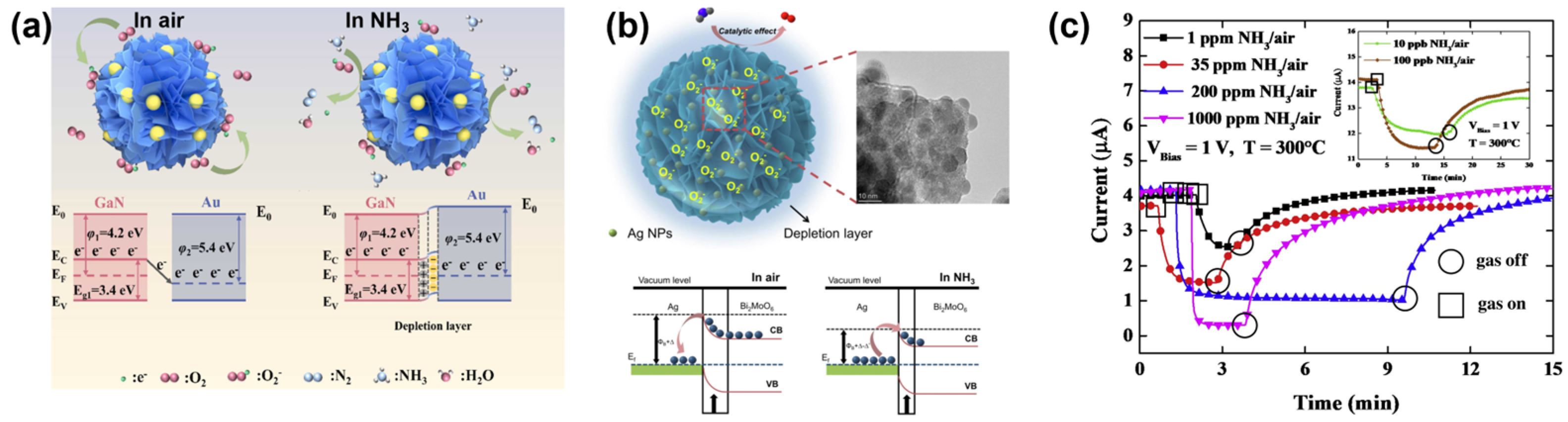
Noble metal decoration mainly uses its excellent catalytic activity and Schottky junction formation between metal and semiconductor to improve the ammonia sensing properties. Non-noble metals mainly improved ammonia sensing properties by adjusting the lattice defects and changing the crystal phase on the basis of the original nanostructure. The composition of composite nanomaterials can form heterogeneous structures between different nanomaterials and make full use of the unique characteristics of each material and their synergistic effects to greatly improve the ammonia sensing performance, which will be the main research direction of sensitive materials for resistive ammonia sensors in the future. The Schottky junction increases the adsorption activity of the gas molecules by changing the interfacial barriers and improves the selectivity and stability of the sensor for ammonia gas. The enhanced selectivity of this design for specific gases reduces interference from other gases, resulting in more accurate detection results. The noble metal Schottky junction enhances the accuracy of the output signal, allowing the circuit to further optimize the ammonia response through signal processing and filtering methods, while increasing the circuit’s immunity to non-target gases. These features help optimize subsequent circuit design and improve the performance of the signal processing circuit.
(3)
The architectural design of interface circuits significantly enhances the flexibility of signal processing while mitigating errors associated with leakage current, series resistance, and system nonlinearity within the digital domain. Furthermore, the precision of the analog reference voltage of the analog-to-digital converter (ADC) in this system does not compromise measurement accuracy. The capability to accurately assess resistance, power dissipation, and ambient temperature of resistive sensors renders this readout architecture particularly suitable for its intended applications.
(4)
The programmable interface circuitry of the MOS gas sensor array encompasses sensor configuration, signal acquisition, data processing, and the output of identification results. This interface circuit is characterized by a highly integrated analog front end (AFE) and a high-performance Cortex-M0 processor. Furthermore, the interface circuit is capable of virtualizing additional MOS gas sensors through rapid temperature control and incorporates the k-nearest neighbor classification algorithm, enabling precise identification of gas types during the thermal runaway process.
The research results in this paper provide a theoretical basis and technical support for the design of high-performance MOS ammonia sensors and lay the foundation for future application promotion. We believe that with the continuous development of materials science and electronic engineering, MOS-based ammonia sensors will be more widely used in the fields of environmental monitoring, industrial safety, and medical health.

Author Contributions

Conceptualization, Y.Y.; methodology, Y.Y.; formal analysis, Z.P.; investigation, J.X., Z.P. and Y.G.; resources, Z.J.; writing—original draft preparation, Y.Y.; writing—review and editing, J.X., Z.J. and Q.X.; visualization, L.J.; supervision, Y.G.; project administration, Q.X.; funding acquisition, Z.J. All authors have read and agreed to the published version of the manuscript.

Funding

This research was funded by Key Scientific and Technological Research Projects in Higher Education Institutions in Hebei Province, grant number ZD2022106.

Data Availability Statement

“Data available in a publicly accessible repository”—The data presented in this study are openly available in [Science Core Collection, e.g., Figure 2a Share] at [doi: 10.1016/j.matlet.2023.133897], reference number [51].

Conflicts of Interest

Authors Yingzhan Yan, Jing Xu, Zhilong Peng, Yuan Gao, Lu Jia and Qian Xu were employed by the company Information Science Academy of China Electronics Technology Group Corporation. The remaining authors declare that the research was conducted in the absence of any commercial or financial relationships that could be construed as a potential conflict of interest.

References

  1. Srirattanapibul, S.; Nakarungsee, P.; Issro, C.; Tang, I.M.; Thongmee, S. Performance of NiO intercalated rGO nanocomposites for NH3 sensing at room temperature. Mater. Sci. Semicond. Process. 2022, 137, 106221. [Google Scholar] [CrossRef]
  2. Erwiha, G.M.; Ham, J.; Sukor, A.; Wickham, A.; Davis, J.G. Organic Fertilizer Source and Application Method Impact Ammonia Volatilization. Commun. Soil Sci. Plant Anal. 2020, 51, 1469–1482. [Google Scholar] [CrossRef]
  3. Afif, A.; Radenahmad, N.; Cheok, Q.; Shams, S.; Kim, J.H.; Azad, A.K. Ammonia-fed fuel cells: A comprehensive review. Renew. Sustain. Energy Rev. 2016, 60, 822–835. [Google Scholar] [CrossRef]
  4. Li, X.; Zhang, X.; Everitt, H.O.; Liu, J. Light-Induced Thermal Gradients in Ruthenium Catalysts Significantly Enhance Ammonia Production. Nano Lett. 2019, 19, 1706–1711. [Google Scholar] [CrossRef]
  5. Lima, A.A.S.; Leite, G.D.N.P.; Ochoa, A.A.V.; Santos, C.A.C.D.; Costa, J.A.P.D.; Michima, P.S.A.; Caldas, A.M.A. Absorption Refrigeration Systems Based on Ammonia as Refrigerant Using Different Absorbents: Review and Applications. Energies 2020, 14, 48. [Google Scholar] [CrossRef]
  6. Lin, X.; Jin, Y.; Yao, J.; Sun, X.; Tian, T.; Li, Z.; Chen, S.; Jiang, J.; Hu, W.; Hao, Y.; et al. Adverse prognosis of nasopharyngeal carcinoma following long-term exposure to multiple air pollutants. Environ. Chem. Lett. 2024, 22, 21–27. [Google Scholar] [CrossRef]
  7. Wu, Y.; Gu, B.; Erisman, J.W.; Reis, S.; Fang, Y.; Lu, X.; Zhang, X. PM2.5 pollution is substantially affected by ammonia emissions in China. Environ. Pollut. 2016, 218, 86–94. [Google Scholar] [CrossRef]
  8. Lin, J.-H.; Yang, T.; Zhang, X.; Shiu, B.-C.; Lou, C.-W.; Li, T.-T. Mn-doped ZnO/SnO2-based yarn sensor for ammonia detection. Ceram. Int. 2023, 49, 34431–34439. [Google Scholar] [CrossRef]
  9. Cao, J.; Zhou, J.; Zhang, Y.; Wang, Y.; Liu, X. Dominating Role of Aligned MoS2/Ni3S2 Nanoarrays Supported on Three-Dimensional Ni Foam with Hydrophilic Interface for Highly Enhanced Hydrogen Evolution Reaction. ACS Appl. Mater. Interfaces 2018, 10, 1752–1760. [Google Scholar] [CrossRef]
  10. Chen, J.; Cao, J.; Zhou, J.; Zhang, Y.; Li, M.; Wang, W.; Liu, J.; Liu, X. Mechanism of highly enhanced hydrogen storage by two-dimensional 1T′ MoS2. Phys. Chem. Chem. Phys. 2020, 22, 430–436. [Google Scholar] [CrossRef]
  11. Schwab, J.J.; Li, Y.; Bae, M.-S.; Demerjian, K.L.; Hou, J.; Zhou, X.; Jensen, B.; Pryor, S.C. A Laboratory Intercomparison of Real-Time Gaseous Ammonia Measurement Methods. Environ. Sci. Technol. 2007, 41, 8412–8419. [Google Scholar] [CrossRef] [PubMed]
  12. Yamamoto, N.; Nishiura, H.; Honjo, T.; Ishikawa, Y.; Suzuki, K. Continuous Determination of Atmospheric Ammonia by an Automated Gas Chromatographic System. Anal. Chem. 1994, 66, 756–760. [Google Scholar] [CrossRef]
  13. Martins, M.R.; Sarkis, L.F.; Sant, S.A.C.; Santos, C.A.; Araujo, K.E.; Santos, R.C.; Araujo, E.S.; Alves, B.J.R.; Jantalia, C.P.; Boddey, R.M.; et al. Optimizing the use of open chambers to measure ammonia volatilization in field plots amended with urea. Pedosphere 2021, 31, 243–254. [Google Scholar] [CrossRef]
  14. Aarya, S.; Kumar, Y.; Chahota, R.K. Recent Advances in Materials, Parameters, Performance and Technology in Ammonia Sensors: A Review. J. Inorg. Organomet. Polym. Mater. 2020, 30, 269–290. [Google Scholar] [CrossRef]
  15. Cao, J.; Zhou, J.; Li, M.; Chen, J.; Zhang, Y.; Liu, X. Insightful understanding of three-phase interface behaviors in 1T-2H MoS2/CFP electrode for hydrogen evolution improvement. Chin. Chem. Lett. 2022, 33, 3745–3751. [Google Scholar] [CrossRef]
  16. Yang, B.; Li, X.; Hua, Z.; Li, Z.; He, X.; Yan, R.; Li, Y.; Zhi, Z.; Tian, C. A low cost and high performance NH3 detection system for a harsh agricultural environment. Sens. Actuators B-Chem. 2022, 361, 131675. [Google Scholar] [CrossRef]
  17. Seesaard, T.; Goel, N.; Kumar, M.; Wongchoosuk, C. Advances in gas sensors and electronic nose technologies for agricultural cycle applications. Comput. Electron. Agric. 2022, 193, 106673. [Google Scholar] [CrossRef]
  18. Cao, J.; Zhang, R.; Chen, L.; Wang, D.; Wang, W.; Tan, E.; Meng, X.; Xiu, H.; Wang, L.; Yang, X.; et al. Design strategies and applications of responsive metal-based luminescence probes in the bioanalysis. TrAC-Trends Anal. Chem. 2023, 168, 117338. [Google Scholar] [CrossRef]
  19. Huang, J.; Jiang, D.; Zhou, J.; Ye, J.; Sun, Y.; Li, X.; Geng, Y.; Wang, J.; Du, Y.; Qian, Z. Visible light-activated room temperature NH3 sensor base on CuPc-loaded ZnO nanorods. Sens. Actuators B-Chem. 2021, 327, 128911. [Google Scholar] [CrossRef]
  20. Qin, Y.; Gui, H.; Bai, Y.; Liu, S. Enhanced NH3 sensing performance at ppb level derived from Ti3C2Tx-supported ZnTi-LDHs nanocomposite with similar metal-semiconductor heterostructure. Sens. Actuators B-Chem. 2022, 352, 131077. [Google Scholar] [CrossRef]
  21. Wang, J.; Yang, J.; Chen, D.; Jin, L.; Li, Y.; Zhang, Y.; Xu, L.; Guo, Y.; Lin, F.; Wu, F. Gas Detection Microsystem with MEMS Gas Sensor and Integrated Circuit. IEEE Sens. J. 2018, 18, 6765–6773. [Google Scholar] [CrossRef]
  22. Fernández-Ramos, M.D.; Capitán-Vallvey, L.F.; Pastrana-Martínez, L.M.; Morales-Torres, S.; Maldonado-Hódar, F.J. Chemoresistive NH3 gas sensor at room temperature based on the carbon gel-TiO2 nanocomposites. Sens. Actuators B Chem. 2022, 368, 132103. [Google Scholar] [CrossRef]
  23. Cao, J.; Wang, W.; Zhou, J.; Chen, J.; Deng, H.; Zhang, Y.; Liu, X. Controllable gas sensitive performance of 1T’ WS2 monolayer instructed by strain: First-principles simulations. Chem. Phys. Lett. 2020, 758, 137921. [Google Scholar] [CrossRef]
  24. Wang, W.; Cao, J.; Zhang, R.; Xiu, H.; Zhang, Y. Room-Temperature NO2 Detection by MoS2-Nanoflake-Decorated AuPt/SnO2 Nanotubes. ACS Appl. Nano Mater. 2023, 6, 17941–17951. [Google Scholar] [CrossRef]
  25. Deng, Z.; Tong, B.; Meng, G.; Liu, H.; Dai, T.; Qi, L.; Wang, S.; Shao, J.; Tao, R.; Fang, X. Insight into the Humidity Dependent Pseudo-n-Type Response of p-CuScO2 toward Ammonia. Inorg. Chem. 2019, 58, 9974–9981. [Google Scholar] [CrossRef] [PubMed]
  26. Nagpal, S.; Nagpal, S. A new model to estimate size distribution from the emission spectra of ZnO nanorods used for highly sensitive ammonia sensors. Pramana-J. Phys. 2022, 96, 83. [Google Scholar] [CrossRef]
  27. Vasiliev, R.; Kurtina, D.; Udalova, N.; Platonov, V.; Nasriddinov, A.; Shatalova, T.; Novotortsev, R.; Li, X.; Rumyantseva, M. SnS= Nanosheets as a Template for 2D SnO2 Sensitive Material: Nanostructure and Surface Composition Effects. Materials 2022, 15, 8213. [Google Scholar] [CrossRef]
  28. Wang, M.; Zeng, Q.; Cao, J.; Chen, D.; Zhang, Y.; Liu, J.; Jia, P. Highly Sensitive Gas Sensor for Detection of Air Decomposition Pollutant (CO, NOx): Popular Metal Oxide (ZnO, TiO2)-Doped MoS2 Surface. ACS Appl. Mater. Interfaces 2024, 16, 3674–3684. [Google Scholar] [CrossRef]
  29. Sivalingam, M.M.; Olmos-Asar, J.A.; Vinoth, E.; Tharmar, T.; Shkir, M.; Said, Z.; Balasubramanian, K. Copper Oxide Nanorod/Reduced Graphene Oxide Composites for NH3 Sensing. ACS Appl. Nano Mater. 2021, 4, 12977–12985. [Google Scholar] [CrossRef]
  30. Su, P.-G.; Zheng, Y.-X. A room temperature NH3 gas sensor based on a quartz crystal microbalance coated with a rGO-SnO2 composite film. Anal. Methods 2022, 14, 1454–1461. [Google Scholar] [CrossRef]
  31. Yin, M.; Yao, Y.; Fan, H.; Liu, S. WO3-SnO2 nanosheet composites: Hydrothermal synthesis and gas sensing mechanism. J. Alloys Compd. 2018, 736, 322–331. [Google Scholar] [CrossRef]
  32. Zhou, Y.; Lin, X.; Huang, Y.; Guo, Y.; Gao, C.; Xie, G.; Jiang, Y. Impact of further thermal reduction on few-layer reduced graphene oxide film and its n-p transition for gas sensing. Sens. Actuators B-Chem. 2016, 235, 241–250. [Google Scholar] [CrossRef]
  33. Choi, Y.R.; Yoon, Y.-G.; Choi, K.S.; Kang, J.H.; Shim, Y.-S.; Kim, Y.H.; Chang, H.J.; Lee, J.-H.; Park, C.R.; Kim, S.Y.; et al. Role of oxygen functional groups in graphene oxide for reversible room-temperature NO2 sensing. Carbon 2015, 91, 178–187. [Google Scholar] [CrossRef]
  34. Štulík, J.; Polansky, R.; Kuberský, P.; Zabelin, D.; Lyutakov, O.; Kolska, Z.; Švorčík, V. Highly Sensitive Ammonia Sensor Based on Modified Nanostructured Polypyrrole Decorated With MAF-6 to Reduce the Effect of Humidity. IEEE Sens. J. 2023, 23, 1896–1907. [Google Scholar] [CrossRef]
  35. Singh, R.; Agrohiya, S.; Rawal, I.; Ohlan, A.; Dahiya, S.; Punia, R.; Maan, A.S. Porous polyaniline/flower-like hybrid phase MoS2/phosphorus-doped graphene ternary nanocomposite for efficient room temperature ammonia sensors. Synth. Met. 2024, 307, 117676. [Google Scholar] [CrossRef]
  36. Xuan, J.; Wang, L.; Zou, Y.; Li, Y.; Zhang, H.; Lu, Q.; Sun, M.; Yin, G.; Zhou, A. Room-temperature gas sensor based on in situ grown, etched and W-doped ZnO nanotubes functionalized with Pt nanoparticles for the detection of low-concentration H2S. J. Alloys Compd. 2022, 922, 166158. [Google Scholar] [CrossRef]
  37. Zhang, R.; Cao, J.; Wang, W.; Tan, E.; Zhu, R.; Chen, W.; Zhang, Y. Research on design strategies and sensing applications of energy storage system based on renewable methanol fuel. Results Eng. 2023, 20, 101439. [Google Scholar] [CrossRef]
  38. Gao, Q.; Dai, Y.; Han, B.; Zhu, W.; Li, X.; Li, C. Enhanced gas-sensitivity and ferromagnetism performances by the Ni-doping induced oxygen vacancies in (Mn, Ni) codoped ZnO nanorods. Appl. Surf. Sci. 2019, 490, 178–187. [Google Scholar] [CrossRef]
  39. Zhang, R.; Cao, J.; Wang, W.; Zhou, J.; Chen, J.; Chen, L.; Chen, W.; Zhang, Y. An improved strategy of passive micro direct methanol fuel cell: Mass transport mechanism optimization dominated by a single hydrophilic layer. Energy 2023, 274, 127276. [Google Scholar] [CrossRef]
  40. Chen, H.-I.; Hsiao, C.-Y.; Chen, W.-C.; Chang, C.-H.; Chou, T.-C.; Liu, I.P.; Lin, K.-W.; Liu, W.-C. Characteristics of a Pt/NiO thin film-based ammonia gas sensor. Sens. Actuators B-Chem. 2018, 256, 962–967. [Google Scholar] [CrossRef]
  41. Liu, Y.; Yuan, Z.; Zhang, R.; Ji, H.; Xing, C.; Meng, F. MoO3/SnO2 Nanocomposite-Based Gas Sensor for Rapid Detection of Ammonia. IEEE Trans. Instrum. Meas. 2021, 70, 9514209. [Google Scholar] [CrossRef]
  42. Zhou, J.; Cao, J.; Zhang, Y.; Liu, J.; Chen, J.; Li, M.; Wang, W.; Liu, X. Overcoming undesired fuel crossover: Goals of methanol-resistant modification of polymer electrolyte membranes. Renew. Sustain. Energy Rev. 2021, 138, 110660. [Google Scholar] [CrossRef]
  43. Hizam, S.M.M.; Al-Dhahebi, A.M.; Saheed, M.S.M. Recent Advances in Graphene-Based Nanocomposites for Ammonia Detection. Polymers 2022, 14, 5125. [Google Scholar] [CrossRef] [PubMed]
  44. Kim, T.; Lee, T.H.; Park, S.Y.; Eom, T.H.; Cho, I.; Kim, Y.; Kim, C.; Lee, S.A.; Choi, M.-J.; Suh, J.M.; et al. Drastic Gas Sensing Selectivity in 2-Dimensional MoS2 Nanoflakes by Noble Metal Decoration. ACS Nano 2023, 17, 4404–4413. [Google Scholar] [CrossRef]
  45. Ou, Y.; Zhou, Y.; Guo, Y.; Niu, W.; Wang, Y.; Jiao, M.; Gao, C. 2D/2D Dy2O3 Nanosheet/MoO3 Nanoflake Heterostructures for Humidity-Independent and Sensitive Ammonia Detection. ACS Sens. 2023, 8, 4253–4263. [Google Scholar] [CrossRef]
  46. Ding, Y.; Guo, X.; Du, B.; Hu, X.; Yang, X.; He, Y.; Zhou, Y.; Zang, Z. Low-operating temperature ammonia sensor based on Cu2O nanoparticles decorated with p-type MoS2 nanosheets. J. Mater. Chem. C 2021, 9, 4838–4846. [Google Scholar] [CrossRef]
  47. Yang, B.; Li, X.; Yuan, W.; Li, Z.; Lu, N.; Wang, S.; Wu, Y.; Fan, S.; Hua, Z. Efficient NH3 Detection Based on MOS Sensors Coupled with Catalytic Conversion. ACS Sens. 2020, 5, 1838–1848. [Google Scholar] [CrossRef]
  48. Ahmad, S.; Khan, I.; Husain, A.; Khan, A.; Asiri, A.M. Electrical Conductivity Based Ammonia Sensing Properties of Polypyrrole/MoS2 Nanocomposite. Polymers 2020, 12, 3047. [Google Scholar] [CrossRef]
  49. Hu, K.; Cai, Y.; Wang, Z.; Zhang, Z.; Xian, J.; Zhang, C. A Review on Metal Oxide Semiconductor-Based Chemo-Resistive Ethylene Sensors for Agricultural Applications. Chemosensors 2024, 12, 13. [Google Scholar] [CrossRef]
  50. Li, Z.; Li, H.; Wu, Z.; Wang, M.; Luo, J.; Torun, H.; Hu, P.; Yang, C.; Grundmann, M.; Liu, X.; et al. Advances in designs and mechanisms of semiconducting metal oxide nanostructures for high-precision gas sensors operated at room temperature. Mater. Horiz. 2019, 6, 470–506. [Google Scholar] [CrossRef]
  51. Kumar, V.; Mirzaei, A.; Bonyani, M.; Kim, K.-H.; Kim, H.W.; Kim, S.S. Advances in electrospun nanofiber fabrication for polyaniline (PANI)-based chemoresistive sensors for gaseous ammonia. TrAC Trends Anal. Chem. 2020, 129, 115938. [Google Scholar] [CrossRef]
  52. Szary, M.J. Toward high selectivity of sensor arrays: Enhanced adsorption interaction and selectivity of gas detection (N2, O2, NO, CO, CO2, NO2, SO2, AlH3, NH3, and PH3) on transition metal dichalcogenides (MoS2, MoSe2, and MoTe2). Acta Mater. 2024, 274, 120016. [Google Scholar] [CrossRef]
  53. Zhang, G.; Wang, B.; Yang, X.; Cao, F.; Xu, H.; Zhou, Y.; Jian, X.; Wang, X. The precise fluorination of ginkgo leaves for enhanced performance of lithium primary batteries. Mater. Lett. 2022, 324, 132812. [Google Scholar] [CrossRef]
  54. Jian, L.; Peng, R.; He, Y.; Wang, X.; Guo, W. One-step hydrothermal synthesis of urchin-like WO3 with excellent ammonia gas sensing property. Mater. Lett. 2023, 336, 133897. [Google Scholar] [CrossRef]
  55. Wang, C.-Y.; Zhang, X.; Rong, Q.; Hou, N.-N.; Yu, H.-Q. Ammonia sensing by closely packed WO3 microspheres with oxygen vacancies. Chemosphere 2018, 204, 202–209. [Google Scholar] [CrossRef]
  56. Xu, Y.; Zeng, W.; Li, Y. A novel seawave-like hierarchical WO3 nanocomposite and its ammonia gas properties. Mater. Lett. 2019, 248, 86–88. [Google Scholar] [CrossRef]
  57. Wang, J.; Zhou, Y.; Zhou, H.; Wangyang, Q.; Peng, Y.; Wangyang, P.; Gu, L. Durian-like NiO architectures as an ultra-sensitive sensing materials for ammonia in normal temperature. Ceram. Int. 2019, 45, 1219–1226. [Google Scholar] [CrossRef]
  58. Zhao, K.; Li, X.; Tang, J.; Yang, H.; Wu, Q.; Wang, X.; Guo, X.; Zeng, D. Effect of exposed facet determined the room-temperature ammonia gas sensing of Cu2O nanoparticles. Appl. Surf. Sci. 2023, 613, 156008. [Google Scholar] [CrossRef]
  59. Wei, W.; Li, W.; Wang, L. High-selective sensitive NH3 gas sensor: A density functional theory study. Sens. Actuators B-Chem. 2018, 263, 502–507. [Google Scholar] [CrossRef]
  60. Alwan, A.M.; Abed, H.R.; Yousif, A.A. Effect of the Deposition Temperature on Ammonia Gas Sensing Based on SnO2/Porous Silicon. Plasmonics 2021, 16, 501–509. [Google Scholar] [CrossRef]
  61. Buyukkose, S. Highly selective and sensitive WO3 nanoflakes based ammonia sensor. Mater. Sci. Semicond. Process. 2020, 110, 104969. [Google Scholar] [CrossRef]
  62. Jha, R.K.; Singh, V.; Sinha, J.; Avasthi, S.; Bhat, N. CVD Grown Cuprous Oxide Thin Film Based High Performance Chemiresistive Ammonia Gas Sensors. IEEE Sens. J. 2019, 19, 11759–11766. [Google Scholar] [CrossRef]
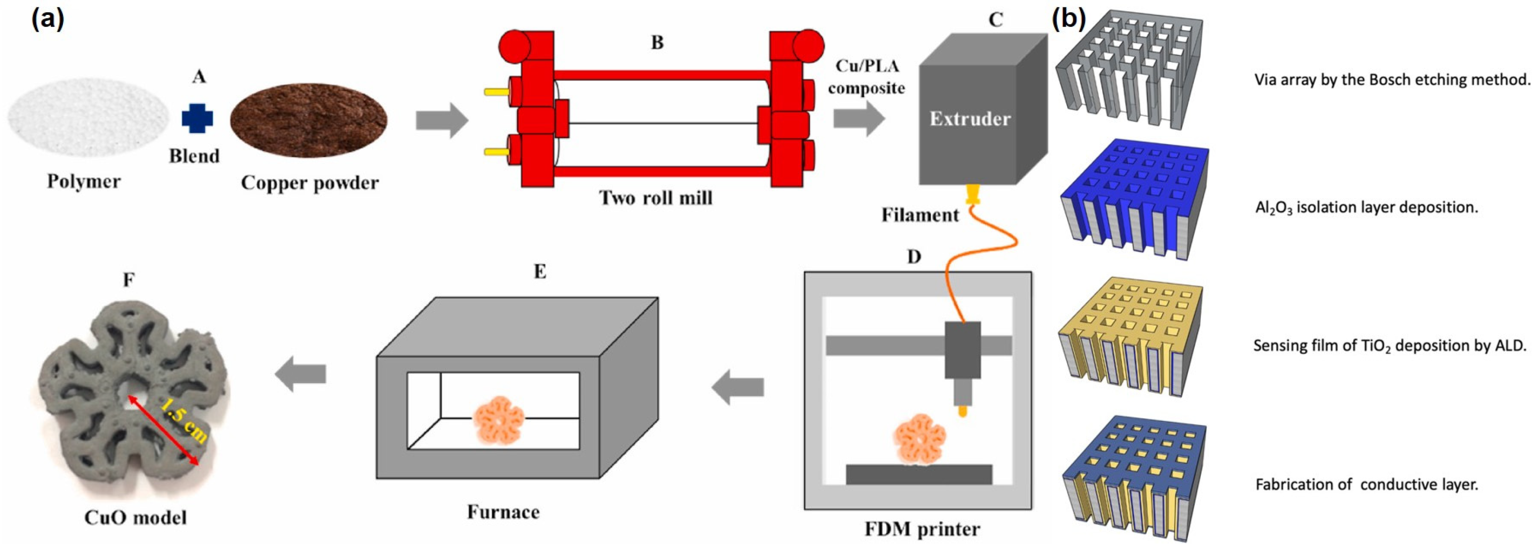
  63. Chaloeipote, G.; Prathumwan, R.; Subannajui, K.; Wisitsoraat, A.; Wongchoosuk, C. 3D printed CuO semiconducting gas sensor for ammonia detection at room temperature. Mater. Sci. Semicond. Process. 2021, 123, 105546. [Google Scholar] [CrossRef]
  64. Yeh, Y.-M.; Chang, S.-J.; Wang, P.H.; Hsueh, T.-J. A Room-Temperature TiO=-based Ammonia Gas Sensor with Three-Dimensional Through-Silicon-Via Structure. ECS J. Solid State Sci. Technol. 2022, 11, 067002. [Google Scholar] [CrossRef]
  65. Yang, F.; Zheng, M.; Zhao, L.; Guo, J.; Zhang, B.; Gu, G.; Cheng, G.; Du, Z. The high-speed ultraviolet photodetector of ZnO nanowire Schottky barrier based on the triboelectric-nanogenerator-powered surface-ionic-gate. Nano Energy 2019, 60, 680–688. [Google Scholar] [CrossRef]
  66. Choi, Y.M.; Cho, S.-Y.; Jang, D.; Koh, H.-J.; Choi, J.; Kim, C.-H.; Jung, H.-T. Ultrasensitive Detection of VOCs Using a High-Resolution CuO/Cu2O/Ag Nanopattern Sensor. Adv. Funct. Mater. 2019, 29, 1808319. [Google Scholar] [CrossRef]
  67. Fu, S.; Zheng, Y.; Zhou, X.; Ni, Z.; Xia, S. Visible light promoted degradation of gaseous volatile organic compounds catalyzed by Au supported layered double hydroxides: Influencing factors, kinetics and mechanism. J. Hazard. Mater. 2019, 363, 41–54. [Google Scholar] [CrossRef] [PubMed]
  68. Cui, X.; Wang, J.; Liu, B.; Ling, S.; Long, R.; Xiong, Y. Turning Au Nanoclusters Catalytically Active for Visible-Light-Driven CO2 Reduction through Bridging Ligands. J. Am. Chem. Soc. 2018, 140, 16514–16520. [Google Scholar] [CrossRef]
  69. Han, D.; Chen, Y.; Li, D.; Shi, J.; Wang, H.; He, X.; Zhao, L.; Wang, W.; Sang, S.; Ji, J. Au nanoparticles decorated GaN nanoflowers with enhanced NH3 sensing performance at room temperature. Sens. Actuators B-Chem. 2023, 394, 134320. [Google Scholar] [CrossRef]
  70. Liu, S.; Qin, Y.; Xie, J. Tuning reactivity of Bi2MoO6 nanosheets sensors toward NH3 via Ag doping and nanoparticle modification. J. Colloid Interface Sci. 2022, 625, 879–889. [Google Scholar] [CrossRef]
  71. Zheng, Y.; Li, M.; Wen, X.; Ho, H.-P.; Lu, H. Nanostructured ZnO/Ag Film Prepared by Magnetron Sputtering Method for Fast Response of Ammonia Gas Detection. Molecules 2020, 25, 1899. [Google Scholar] [CrossRef] [PubMed]
  72. Qiu, Z.; Tian, X.; Li, Y.; Zeng, Y.; Fan, C.; Wang, M.; Hua, Z. NH3 sensing properties and mechanism of Ru-loaded WO3 nanosheets. J. Mater. Sci.-Mater. Electron. 2018, 29, 11336–11344. [Google Scholar] [CrossRef]
  73. Dai, Y.-Z.; Liang, S.-Y.; Lv, C.; Wang, G.; Xia, H.; Zhang, T.; Sun, H.-B. Controllably fabricated single microwires from Pd-WO3•xH2O nanoparticles by femtosecond laser for faster response ammonia sensors at room temperature. Sens. Actuators B-Chem. 2020, 316, 128122. [Google Scholar] [CrossRef]
  74. Garshev, A.V.; Ivanov, V.K.; Krotova, A.A.; Filatova, D.G.; Konstantinovac, E.A.; Naberezhnyi, D.O.; Khmelevsky, N.O.; Marikutsa, A.V.; Kots, P.A.; Smirnov, A.V.; et al. Enhancement of Lewis Acidity of Cr-Doped Nanocrystalline SnO2: Effect on Surface NH3 Oxidation and Sensory Detection Pattern. ChemPhysChem 2019, 20, 1985–1996. [Google Scholar] [CrossRef] [PubMed]
  75. Sun, J.; Wang, Y.; Song, P.; Yang, Z.; Wang, Q. Metal-organic framework-derived Cr-doped hollow In2O3 nanoboxes with excellent gas-sensing performance toward ammonia. J. Alloys Compd. 2021, 879, 160472. [Google Scholar] [CrossRef]
  76. Li, Y.-Y.; Chen, J.-L.; Gong, F.-L.; Jin, G.-X.; Xie, K.-F.; Yang, X.-Y.; Zhang, Y.-H. Dual functionalized Ni substitution in shuttle-like In2O3 enabling high sensitivity NH3 detection. Appl. Surf. Sci. 2022, 600, 154158. [Google Scholar] [CrossRef]
  77. Vorobyeva, N.; Rumyantseva, M.; Platonov, V.; Filatova, D.; Chizhov, A.; Marikutsa, A.; Bozhev, I.; Gaskov, A. Ga2O3(Sn) Oxides for High-Temperature Gas Sensors. Nanomaterials 2021, 11, 2938. [Google Scholar] [CrossRef]
  78. Varudkar, H.A.; Umadevi, G.; Nagaraju, P.; Dargad, J.S.; Mote, V.D. Fabrication of Al-doped ZnO nanoparticles and their application as a semiconductor-based gas sensor for the detection of ammonia. J. Mater. Sci.-Mater. Electron. 2020, 31, 12579–12585. [Google Scholar] [CrossRef]
  79. Yao, G.; Yu, J.; Wu, H.; Li, Z.; Zou, W.; Zhu, H.; Huang, Z.; Huang, H.; Tang, Z. P-type Sb doping hierarchical WO3 microspheres for superior close to room temperature ammonia sensor. Sens. Actuators B-Chem. 2022, 359, 131365. [Google Scholar] [CrossRef]
  80. Zhu, H.; Ji, H.; Yuan, Z.; Shen, Y.; Gao, H.; Meng, F. Highly selective room temperature ammonia gas sensors based on d-band C-SnO2 and response behavior induced by oxidative and reductive role shifts. J. Mater. Chem. A 2023, 11, 10565–10576. [Google Scholar] [CrossRef]
  81. Sadhanala, H.K.; Nandan, R.; Nanda, K.K. Understanding the ammonia sensing behavior of filter coffee powder derived N-doped carbon nanoparticles using the Freundlich-like isotherm. J. Mater. Chem. A 2016, 4, 8860–8865. [Google Scholar] [CrossRef]
  82. Liu, M.; Sun, R.-Y.; Ding, Y.-L.; Wang, Q.; Song, P. Au/α-Fe2O3/Ti3C2Tx MXene Nanosheet Heterojunctions for High-Performance NH3 Gas Detection at Room Temperature. ACS Appl. Nano Mater. 2023, 6, 11856–11867. [Google Scholar] [CrossRef]
  83. Peng, R.; Li, Y.; Liu, T.; Sun, Q.; Si, P.; Zhang, L.; Ci, L. Reduced graphene oxide/SnO2@Au heterostructure for enhanced ammonia gas sensing. Chem. Phys. Lett. 2019, 737, 136829. [Google Scholar] [CrossRef]
  84. Pang, Z.; Nie, Q.; Lv, P.; Yu, J.; Huang, F.; Wei, Q. Design of flexible PANI-coated CuO-TiO2-SiO2 heterostructure nanofibers with high ammonia sensing response values. Nanotechnology 2017, 28, 225501. [Google Scholar] [CrossRef] [PubMed]
  85. Yuan, Z.; Liu, Y.; Zhang, J.; Meng, F.; Zhang, H. Rose-Like MoO3/MoS2/rGO Low-Temperature Ammonia Sensors Based on Multigas Detection Methods. IEEE Trans. Instrum. Meas. 2021, 70, 9506109. [Google Scholar] [CrossRef]
  86. Bera, S.; Kundu, S.; Khan, H.; Jana, S. Polyaniline coated graphene hybridized SnO2 nanocomposite: Low temperature solution synthesis, structural property and room temperature ammonia gas sensing. J. Alloys Compd. 2018, 744, 260–270. [Google Scholar] [CrossRef]
  87. Lu, L.; Liu, M.; Sui, Q.; Zhang, C.; Zou, Y.; Xu, F.; Sun, L.; Xiang, C. MXene/MoS2 nanosheet/polypyrrole for high-sensitivity detection of ammonia gas at room temperature. Mater. Today Commun. 2023, 35, 106239. [Google Scholar] [CrossRef]
  88. Abdollahi, H.; Samkan, M.; Hashemi, M.M. Facile and fast electrospinning of crystalline ZnO 3D interconnected nanoporous nanofibers for ammonia sensing application. Microsyst. Technol.-Micro-Nanosyst.-Inf. Storage Process. Syst. 2018, 24, 3741–3749. [Google Scholar] [CrossRef]
  89. He, J.; Liang, B.; Yan, X.; Liu, F.; Wang, J.; Yang, Z.; You, R.; Wang, C.; Sun, P.; Yan, X.; et al. A TPA-DCPP organic semiconductor film-based room temperature NH3 sensor for insight into the sensing properties. Sens. Actuators B-Chem. 2021, 327, 128940. [Google Scholar] [CrossRef]
  90. Park, P.; Ruffieux, D.; Makinwa, K.A.A. A Thermistor-Based Temperature Sensor for a Real-Time Clock With ±2 ppm Frequency Stability. IEEE J. Solid-State Circuits 2015, 50, 1571–1580. [Google Scholar] [CrossRef]
  91. Cai, Z.; Veldhoven, R.H.M.V.; Falepin, A.; Suy, H.; Sterckx, E.; Makinwa, K.A.A.; Pertijs, M.A.P. An integrated carbon dioxide sensor based on ratiometric thermal-conductivity measurement. In Proceedings of the 2015 Transducers—2015 18th International Conference on Solid-State Sensors, Actuators and Microsystems (TRANSDUCERS), Anchorage, AK, USA, 21–25 June 2015; pp. 622–625. [Google Scholar]
  92. Damilano, A.; Hayat, H.M.A.; Bonanno, A.; Demarchi, D.; Crepaldi, M. A Flexible Low-Power 130 nm CMOS Read-Out Circuit with Tunable Sensitivity for Commercial Robotic Resistive Pressure Sensors. IEEE Sens. J. 2015, 15, 6650–6658. [Google Scholar] [CrossRef]
  93. Tadić, N.; Zogović, M.; Gobović, D. A CMOS Controllable Constant-Power Source for Variable Resistive Loads Using Resistive Mirror with Large Load Resistance Dynamic Range. IEEE Sens. J. 2014, 14, 1988–1996. [Google Scholar] [CrossRef]
  94. Chan, S.S.W.; Chan, P.C.H. A resistance-variation-tolerant constant-power heating circuit for integrated sensor applications. IEEE J. Solid-State Circuits 1999, 34, 432–439. [Google Scholar] [CrossRef]
  95. Cai, Z.; Veldhoven, R.H.M.V.; Falepin, A.; Suy, H.; Sterckx, E.; Bitterlich, C.; Makinwa, K.A.A.; Pertijs, M.A.P. A Ratiometric Readout Circuit for Thermal-Conductivity-Based Resistive CO2 Sensors. IEEE J. Solid-State Circuits 2016, 51, 2463–2474. [Google Scholar] [CrossRef]
  96. Cai, Z.; Guerrero, L.E.R.; Louwerse, A.M.R.; Suy, H.; Veldhoven, R.V.; Makinwa, K.A.A.; Pertijs, M.A.P. A CMOS Readout Circuit for Resistive Transducers Based on Algorithmic Resistance and Power Measurement. IEEE Sens. J. 2017, 17, 7917–7927. [Google Scholar] [CrossRef]
  97. Ge, G.; Zhang, C.; Hoogzaad, G.; Makinwa, K.A.A. A Single-Trim CMOS Bandgap Reference with a 3σ Inaccuracy of ±0.15% from −40 °C to 125 °C. IEEE J. Solid-State Circuits 2011, 46, 2693–2701. [Google Scholar] [CrossRef]
  98. Shalmany, S.H.; Draxelmayr, D.; Makinwa, K.A.A. A ±36A Integrated Current-Sensing System With a 0.3% Gain Error and a 400 μA Offset From −55 °C to +85 °C. IEEE J. Solid-State Circuits 2017, 52, 1034–1043. [Google Scholar] [CrossRef]
  99. Saputra, N.; Pertijs, M.A.P.; Makinwa, K.A.A.; Huijsing, J.H. Sigma delta ADC with a dynamic reference for accurate temperature and voltage sensing. In Proceedings of the 2008 IEEE International Symposium on Circuits and Systems (ISCAS), Seattle, WA, USA, 18–21 May 2008; pp. 1208–1211. [Google Scholar]
  100. Meijer, G.C.M. Thermal sensors based on transistors. Sens. Actuators 1986, 10, 103–125. [Google Scholar] [CrossRef]
  101. Pertijs, M.A.P.; Makinwa, K.A.A.; Huijsing, J.H. A CMOS smart temperature sensor with a 3σ inaccuracy of ±0.1 °C from −55 °C to 125 °C. IEEE J. Solid-State Circuits 2005, 40, 2805–2815. [Google Scholar] [CrossRef]
  102. Ren, M.; Xu, H.; Dong, C.; Zhang, Z. Toward a Gas Sensor Interface Circuit—A Review. IEEE Sens. J. 2022, 22, 18253–18265. [Google Scholar] [CrossRef]
  103. Asri, M.I.A.; Hasan, M.N.; Fuaad, M.R.A.; Yunos, Y.M.; Ali, M.S.M. MEMS Gas Sensors: A Review. IEEE Sens. J. 2021, 21, 18381–18397. [Google Scholar] [CrossRef]
  104. Gardner, J.W.; Guha, P.K.; Udrea, F.; Covington, J.A. CMOS Interfacing for Integrated Gas Sensors: A Review. IEEE Sens. J. 2010, 10, 1833–1848. [Google Scholar] [CrossRef]
  105. Kumar, R.; Ghosh, R. Selective determination of ammonia, ethanol and acetone by reduced graphene oxide based gas sensors at room temperature. Sens. Bio-Sens. Res. 2020, 28, 100336. [Google Scholar] [CrossRef]
Figure 1. Number of publications on metal-oxide semiconductor ammonia sensors in recent years.
Electronics 13 04800 g001
Figure 2. Potential barrier at n-type MOS grain.
Electronics 13 04800 g002
Figure 3. The SEM image of (a) urchin-like WO3 (reprinted from Ref. [54]), (b) WO3 microspheres (reprinted from Ref. [55]), (c) seawave-like WO3 (reprinted from Ref. [56]), (d) durian-like NiO (reprinted from Ref. [57]), (e) Cu2O concave octahedrons (reprinted from Ref. [58]), and (f) Co3O4 hexagonal platelets (reprinted from Ref. [59]).
Electronics 13 04800 g003
Figure 4. (a) Fabrication process of 3D printed CuO gas sensor (reprinted from Ref. [63]). (b) Schematic image of the fabrication process for the 3D TSV-structured TiO2 gas sensor (reprinted from Ref. [64]).
Electronics 13 04800 g004
Figure 5. A schematic representation illustrating the ammonia sensing mechanism alongside the energy band structure of the relevant materials is presented. (a) Au-GaN nanoflowers (reprinted from Ref. [69]) and (b) Ag-Bi2MoO6 (reprinted from Ref. [70]). (c) A schematic representation illustrating the ammonia sensing mechanism alongside the energy band structure of the relevant materials is presented. (a) Transient responses of the Pt-NiO at 300 °C under different ammonia concentrations. Reprinted from Ref. [40].
Electronics 13 04800 g005
Figure 6. (a) A visual representation showcasing the charge transfer dynamics and the ammonia vapor detection method utilized by the Sb-WO3 sensor. Reprinted from Ref. [79]. (b) P-type sensing response mechanism of C-SnO2 to ammonia. Reprinted from Ref. [80].
Electronics 13 04800 g006
Figure 7. (a) A comprehensive examination of the gas sensing reaction mechanism in heterostructures is presented, accompanied by a schematic representation of the energy band diagram for SnO2, core-shell structure, and heterostructure. Reprinted from Ref. [83]. (b) Schematic of different heterojunctions formed in the CuO-TiO2-SiO2 composite nanofibers. Reprinted from Ref. [84].
Electronics 13 04800 g007
Figure 8. Block diagram of interface circuit for gas sensor array.
Electronics 13 04800 g008
Table 1. The properties of MOS nanomaterials and other materials.
GasMaterialConc. (a) [ppm]Tem (b) [°C]S (c)τres (d) [s]τrec (e) [s]Ref. (f)
NO2AuPt/SnO252313.16 (h)106[24]
NO2AuPt/SnO2102313.15 (h)208[24]
COZnO-MoS2(g)25(g)(g)0.046[27]
NO2SnO2-NiO(g)30036 (h)204163[28]
NH3CuO50(g)(g)3.876.29[29]
(a) Conc.: Concentration; (b) Tem: Working Temperature; (c) S: Sensitivity; (d) τres: Response Time; (e) τrec: Recovery Time; (f) Ref.: Reference; (g) Not Mentioned; (h) S = Rg/Ra.
Table 2. Detailed performance parameters of resistive ammonia sensors.
MaterialResponse/
Concentration (ppm)
Response Time (s)Recovery Time (s)Stability
(Days)
Lowest Concentration Detected (ppm)Operating TemperatureRef.
WO344.0 (a)/305460-49.55300 °C[54]
WO33.32 (c)/100150210-1350 °C[55]
WO377 (j)/300---50250 °C[56]
NiO40% (i)/506.317.2-15Room temperature[57]
Cu2O0.35 (g)/100--6025Room temperature[58]
Co3O4~1.7 (b)/501262541510Room temperature[59]
Au-Fe3O4~90% (f)/2020701500.25Room temperature[61]
Au-GaN86.8% (f)/100411693072Room temperature[69]
Ag-Bi2MoO637.6 (d)/2005383050Room temperature[70]
Pt-NiO1278% (g)/10001576-10300 °C[40]
Pd-WO3~1.04 (a)/501.43.3161Room temperature[73]
Cr-In2O311 (a)/10118161140 °C[75]
Ni-In2O32732 (a)/502310301140 °C[76]
Sb-WO3~1.22 (b)/51.223.24220035 °C[79]
C-SnO21996% (e)/10037.5105.510100Room temperature[80]
Au-Fe2O3-Ti3C2Tx16.9 (f)/132301Room temperature[82]
Au-rGO-SnO258% (h)/102041305Room temperature[83]
Mn-ZnO-SnO213.13 (a)/10064243010Room temperature[8]
CuO-TiO2-SiO245.67 (g)/100---400Room temperature[84]
MoO3-MoS2-rGO52 (a)/100304301200 °C[85]
(a)  R e s p o n s e = R a R g  (b)  R e s p o n s e = R g R a  (c)  R e s p o n s e = I g I a  (d)  R e s p o n s e = G g G a  (e)  R e s p o n s e = ( R a R g ) R g  (f)  R e s p o n s e = ( R a R g ) R a  (g)  R e s p o n s e = ( R g R a ) R a  (h)  R e s p o n s e = R a R g R a  (i)  R e s p o n s e = ( G a G g ) G a  (j) Not mentioned.
Disclaimer/Publisher’s Note: The statements, opinions and data contained in all publications are solely those of the individual author(s) and contributor(s) and not of MDPI and/or the editor(s). MDPI and/or the editor(s) disclaim responsibility for any injury to people or property resulting from any ideas, methods, instructions or products referred to in the content.

