1. Introduction
When the ZX Spectrum was first released in 1982, it was considered a breakthrough in personal computing, due to its use of commonly available analog TVs and audio cassettes and to its being available at a reasonable price for the average consumer. The capabilities of modern computers and game consoles have long surpassed the ZX Spectrum but there is a generalized interest in reviving some of its games. The main limitation of being able to play ZX Spectrum games is that ZX Spectrum requires an audio cassette player, a TV set with an analog RF tuner, and an original micro-switch joystick, not to mention a computer still in working order. Traditional hardware ZX Spectrum computers have not been manufactured for the past four decades. Moreover, the loading of a game requires an audio tape playing between 5–10 min, which, nowadays, may be too much to ask to wait for.
To avoid the difficulty of having all the hardware of that era in perfect working order, many ZX Spectrum emulators have been created for different platforms, either in software or hardware. Despite this, software emulators tend to have behaviors or glitches caused by the underlying system, which do not exist when running a game on the original ZX Spectrum. Moreover, many of these implementations do not faithfully replicate the operation of the architecture of the original ZX Spectrum. To counter this, a hardware implementation of the ZX Spectrum was made.
This paper proposes and has validated a methodology that can be applied to old systems that are still operational, to upgrade them. This implementation is a means of validating the proposed methodology before applying it to a physical system. Another reason for investigating hardware implementations rather than software ones was to achieve the maximum fidelity with the original ZX Spectrum. Moreover, many hardware implementations of the old computer were developed by retro-gaming communities in ways that are nearly impossible to reproduce and that require the assembly of custom Printed Circuit Boards (PCBs) that may not be available. Field-Programmable Gate Array (FPGA) technology was chosen, due to its easy reconfigurability, testability, integration, and customization, despite allowing a complete system to be programmable within it. The use of an FPGA development kit allowed a hardware design without the need to design and assemble a customized and complex PCB. Research on similar previous works was conducted, to re-use any existing validated IP cores, i.e., the Z80 Central Processing Unit (CPU).
The objective of this work was to recreate a ZX Spectrum+ on a modern hardware platform and to be able to load and play original games as a demonstration of the developed system. This paper details the recreation of a ZX Spectrum+ computer on a modern hardware platform capable of running software exactly as in the original computer while using modern peripherals, such as a Video-Graphics-Array-(VGA) monitor, an SD card for faster game loading and saving, and available retro joysticks. The target hardware platform was the DE2-115 FPGA board from Terasic, which included the connectors and interfaces for the new peripherals. The system supports the following peripherals:
VGA video output, used by common computer monitors;
PS/2 keyboard input and the original ZX Spectrum keyboard;
SD card for faster-loading programs and games;
Audio input for loading audio cassette tapes, allowing old games to be played;
Audio output for playing sounds and music;
Kempston and Sinclair joysticks inputs.
This system additionally supports save-state functionality. This allows the user to create a state of the machine with the press of a button. This state can be used to, for instance, resume a game at a certain point.
This paper is organized as follows:
Section 2 presents the background on the ZX Spectrum computer architecture and previous works on its recreation attempts.
Section 3 is dedicated to presenting the new reconfigurable architecture, which has the original ZX Spectrum’s hardware recreated as well as the new I/O peripherals.
Section 4 presents the results obtained from the implementation of the proposed architecture. The results are discussed in
Section 5, and conclusions are drawn in
Section 6.
2. Background
2.1. The ZX Spectrum+/48K
The ZX Spectrum is an 8-bit home computer that was developed by Sinclair and released in 1982. One of the first models released was the 48K, which had 48 KB of Random-Access Memory (RAM) and 16 KB of Read-Only Memory (ROM). The ZX Spectrum 48K is comprised of a Z80 Zilog CPU, an Uncommited Logic Array (ULA) for interaction with memory modules, and peripherals such as the beeper for sound output, the keyboard, and the video and RF modulators for video output to analog televisions. ZX Spectrum+ models had a different keyboard, but the underlying system remained the same.
The Z80 is a processor with 16 bits of addressing space and an 8-bit data bus. This CPU was widely used by home computers at the time and is still used to this day on Texas Instrument graphing calculators and other low-cost devices [
1]. The Z80 has three modes of maskable interrupts, a non-maskable interrupt, separate control signals for memory, and a separate I/O address space and support for Direct-Memory-Access-(DMA) requests [
2].
The ULA is a semiconductor device from Ferranti that was used to design and produce custom logic chips. It was fabricated with various generic building blocks on the bottom-four metal layers, connected to a top metal layer designed by the customer, to support a custom logic circuit [
3]. The ULA was cheaper than soldering several components on a PCB, thus lowering the cost of the ZX Spectrum. The ULA is responsible for keyboard scanning, reading the data from video memory and sending them to the video modulator, and serving as a peripheral for the Z80 to have access to the audio I/O as well as control over the border color on the screen. It also generates the clock for the Z80 at 3.5 MHz. The ULA controls the Z80 clock, to handle contention between the two video memory accesses. The video takes priority, so if the Z80 and the ULA are both accessing the lower RAM, where the video is also stored (0x4000 to 0x7FFF), the ULA stops the Z80’s clock before the control signals are set [
4]. The ULA receives a 14 MHz clock and divides it internally down to 7 MHz.
The ZX Spectrum’s active screen has a resolution of 256 × 192 pixels or 32 × 24 attribute blocks. Each attribute block is equivalent to a square of 8 × 8 pixels. These blocks can have two colors each, designated “ink” and “paper”, for foreground and background colors, respectively. Color data stored in the RAM specify the color of the INK, PAPER, and brightness of each block, as well as if they are flashing (switching paper and ink colors). Each byte in the video memory corresponds to 8 pixels, where 1 pixel corresponds to 1 bit in that memory position. Its value determines if the color rendered is INK or PAPER. Every group of 32 bytes corresponds to a full row of pixels from left to right on the active screen. The video memory is split into three groups of 8 attribute-block rows, resulting in the 24-block height of the screen [
5].
The keyboard on the ZX Spectrum consists of a matrix with a series of half rows that can be selected with the top byte of the address bus. When the Z80 reads the ULA’s port at 0x7FFE–0xFEFE, it sets the top byte to select a half row and the data received correspond to the state of the keys in that half row, active-low [
6].
2.2. Field-Programmable Gate Array
An FPGA is an integrated circuit that has the ability to reconfigure the hardware inside it, to create a custom logic system. Similarly to ULAs, it is composed of programmable building blocks (logic elements) and interconnects used to create complex digital circuits. Unlike ULAs, it is re-programmable, making it easier to test designs on. It is also more complex than ULAs and can hold more logic elements, as well as memory units and PLLs [
7]. An FPGA can be programmed in Hardware Description Languages, such as VHDL or Verilog.
In this work, a DE2-115 Terasic board was chosen, due to various factors:
Availability: The board was already available in the lab;
Peripherals: The peripherals the board supported were favorable for the implementation;
Less resource concerns: The capacity of the Cyclone IV-E FPGA EP4CE115 from Intel included in the board had more than enough resources to implement ZX Fusion without the need to worry about the lack of space or memory.
The Cyclone IV has 114,000 Logic Elements, 266 DSP Blocks, 3.888 Mb of M9K-(8192 bit)-RAM blocks, and four PLLs [
8]. Each Logic Element is composed of a four-input Look-Up Table (LUT) connected to a carry-chain block followed by a 1-bit register [
9].
Intel’s Quartus prime 18.1 software was used for the development and programming of this implementation on the FPGA. The built-in NIOS II Software Build Tools for Eclipse was used for NIOS’ programming, in C.
2.3. Related Work
In the scope of the work proposed in this paper, the most relevant ZX Spectrum implementations found for FPGA were analyzed, to determine if any IP blocks or unique features could be re-used. Some of the implementations investigated included:
3. Modernized Architecture
The proposed architecture to modernize outdated computing systems like the ZX Spectrum+ relies on a co-processor attached to the address/data buses to issue memory access requests and occasionally control the Z80 CPU.
The target FPGA is an Intel Cyclone IV. In this work, a soft co-processor was used as a bridge between the ZX Spectrum and the peripherals that it could not support with its original architecture, such as loading and saving files from/to an SD card. In this case, the co-processor was materialized on a NIOS II from Intel [
17], which could be instanced in the FPGA. To load and save programs, the software on the NIOS II supported .Z80 and .SNA files stored on an SD card with FAT32 or FAT16. The NIOS II processor interpreted and decoded the files before writing their contents directly to memory. In addition to the SD-card access, the NIOS II was also responsible for the contents of the new menu for loading files.
3.1. High-Level System Architecture
A diagram of the general architecture of this implementation is illustrated in
Figure 1. The blue rectangles are used to represent I/O interfaces and the green ones are custom IP cores that did not exist in the original ZX Spectrum+.
3.2. Z80 CPU
As aforementioned, the Z80 is the heart of the ZX Spectrum+. This work used the implementation from T80 [
18]. It was chosen for being extensively tested and used in several projects. To test the T80 CPU, a minimal system was created. It included a ROM and three RAM modules (Screen, Color, and Data). The Video RAM (VRAM) (Screen and Color RAM) was implemented with dual-port RAMs, to have the CPU and the VGA controller accessing the memories simultaneously.
3.3. ULA
The ULA in the original ZX Spectrum was responsible for reading the video data and sending them to the video modulator. As it was no longer needed, it was reduced to two IP blocks:
ULA Ports based on [
11], which acted as the peripheral of the Z80, providing access to the keyboard and audio and keeping track of the border color;
ULA counter—new video counters (horizontal, vertical, and flash) with outputs that could trigger the T80’s interrupt, generate the T80’s clock, stop it for contention handling, and output the flash clock for the video component.
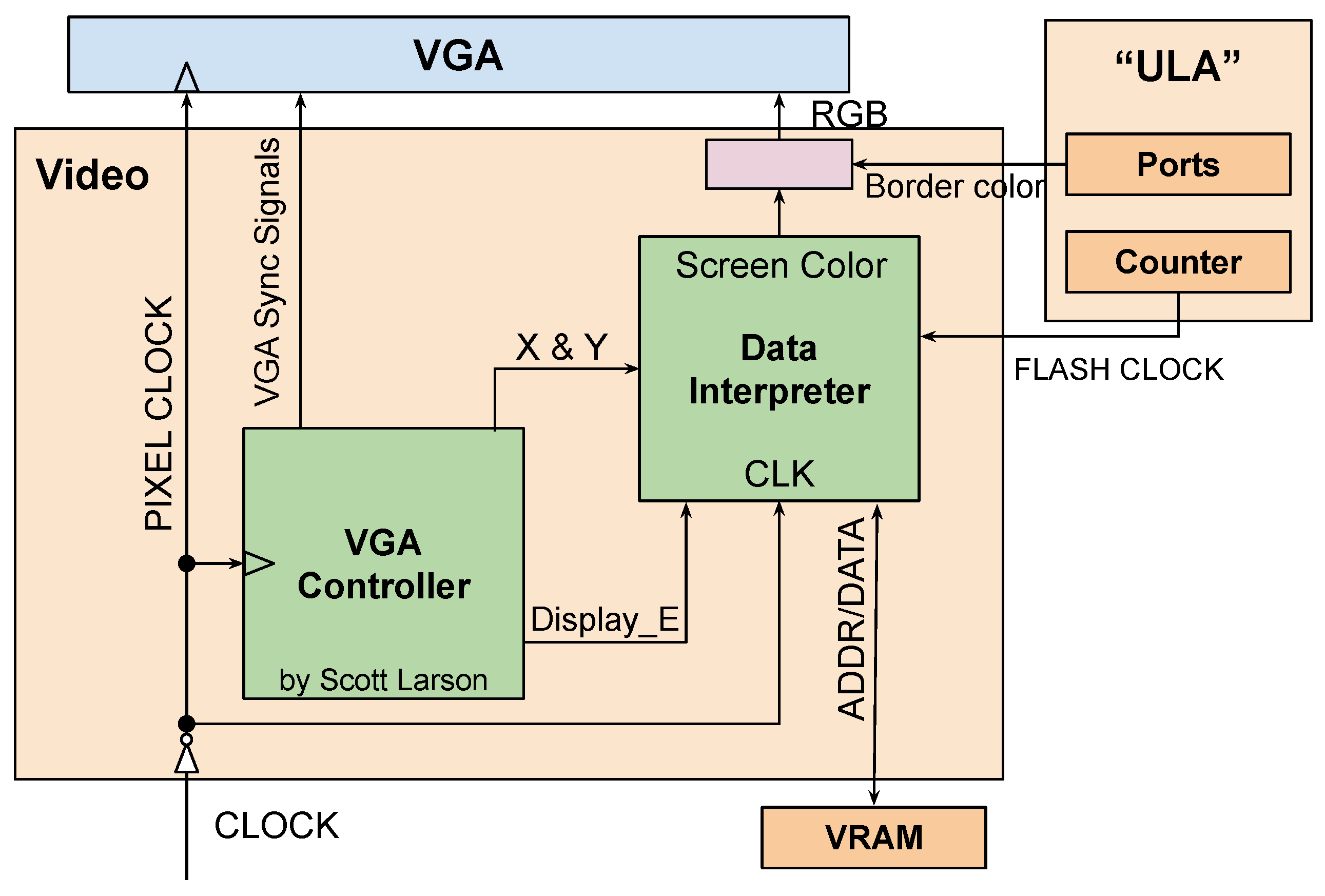
3.4. Video Output
The video output resolution was 1024 × 768, which is supported by most modern monitors. It is also a multiple of 4 of the original ZX Spectrum’s active screen resolution (256 × 192). The video controller was also capable of producing 1× and 2× scaling factors, making the visible area smaller and the border larger. A VGA signal of 1024 × 768 at 60 Hz requires a pixel clock of 65 MHz, which is greater than the ULA’s internal clock of 7 MHz. With this resolution, the border is only 1-pixel thick at the edge of the screen. If the user prefers having a larger border, two other video modes can be set with the switches SW[0] and SW[1] on the board. The architecture of the video component is illustrated in
Figure 2.
The VGA Controller from [
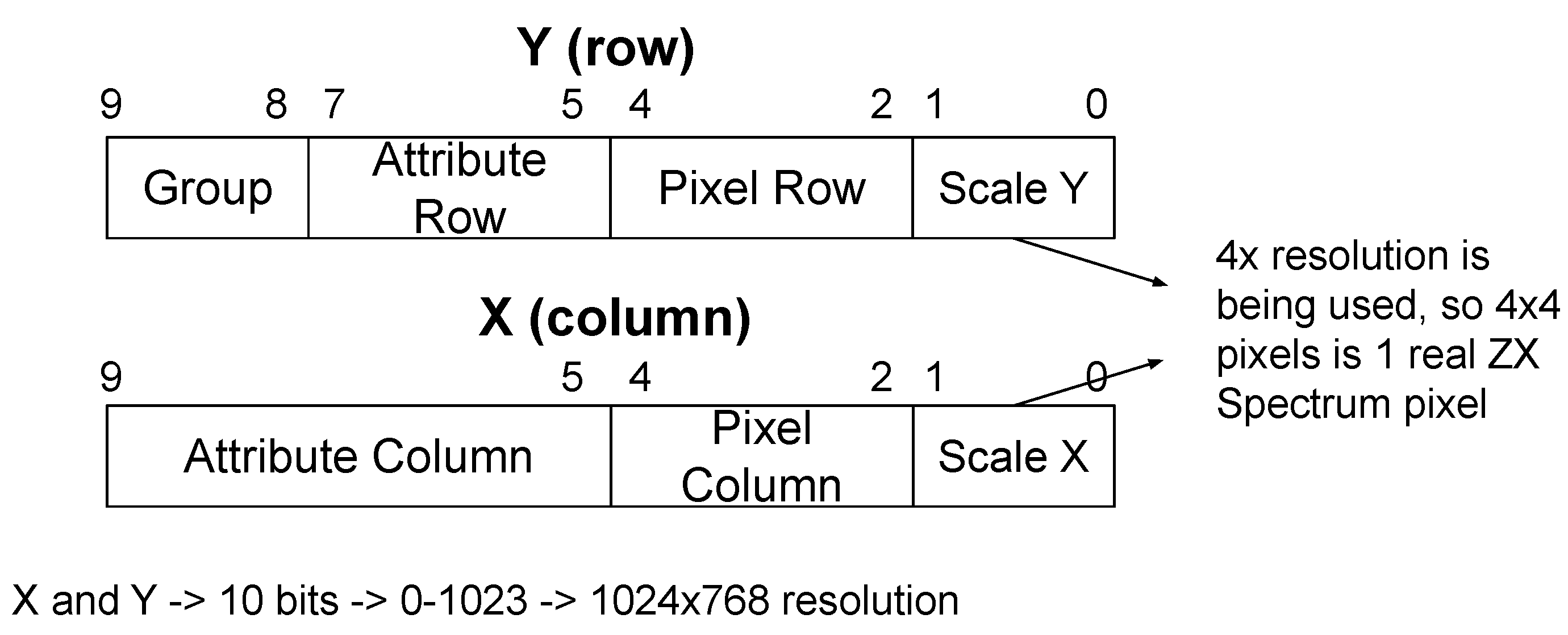
19] received the video clock and generated the VGA’s sync signals as well as the current row and column that was being drawn. The Data Interpreter received these row and column numbers and calculated the addresses of the current screen and color info being rendered. The VRAM was driven by a clock with the opposite polarity of the video clock, so that new video data were fetched when the current data were being displayed. The VRAM memory addresses were computed from the row and column values, as seen in
Figure 3. The computations are in Equations (
1) and (
2):
and
3.5. PS/2 and Original ZX Spectrum+ Keyboards
As original ZX Spectrum+ keyboards are becoming scarce and the DE2-115 FPGA board has a PS/2 connector, it was used to connect a keyboard to the system. The keyboard IP Block consisted of a PS/2 Controller from [
20] and what was called an “Input Receiver”. The PS/2 Controller supported bidirectional communication with the keyboard. It received key codes and sent LED state updates. The “Input Receiver” received the top byte of the address bus and the key codes of keys that were pressed or released and, according to them, output data that corresponded to those key presses, depending on the half rows selected by the address bits. The state of the shift and alt keys were considered for shortcuts in US and PT keyboards and trigger combinations of CAPS SHIFT and SYMB SHIFT to write the specific symbols.
A native ZX Spectrum+ keyboard could be selected by activating switching SW[16] on the target platform. This connected the top address byte and the 5-bit data bus directly to the keyboard. If the Sinclair mode was on for the joysticks (SW[17] off), the controller’s state was de-serialized in the IP block “nes_gamepad” and interpreted as the half rows they corresponded to, 1-5 or 6-0, as Sinclair joysticks would map to these keys.
3.6. Audio I/O
The audio input and output were supported by a WM8731 codec from Wolfson on the target platform. The codec was configured for a reference clock of 18.432 MHz (same value as in the datasheet [
21]), a sample rate of 48 KHz, a 1-bit datawidth, and a channel number of 2, for stereo audio. The calculation was as follows:
It should be noted that the audio output of the ZX Spectrum is done with only 1 bit, so the bit clock would be appropriate for this. LRCK uses only the sample rate and the reference clock in its calculation, similarly. The calculation was as follows:
These calculations, with the aforementioned constants, resulted in 192000-1 and 96000-1 for BCLK and LRCK, respectively. The stereo clock was half of the bit clock, as the bit clock was calculated for a data width of 1, meaning the stereo clock had to change for every period of the bit clock.
The audio output of the ZX Spectrum was sent as data directly to the CODEC and the generated clocks transmitted them successfully.
Audio input, however, required transformation, due to the CODEC being 24-bit. This meant having to translate the 24-bit value into a 1-bit value for the ZX Spectrum input. A component was made called “audio_adc”, which contained a 4-bit counter and a 24-bit shift register that received the data sent by the CODEC. To facilitate the conversion, only the MSB was sent to the EAR input of the ULA, so that when the 24th bit was received the MSB changes and the ULA received it. This meant that values 0x000000–0x7FFFFF are interpreted as 0, whilst values 0x800000–0xFFFFFF are interpreted as 1.
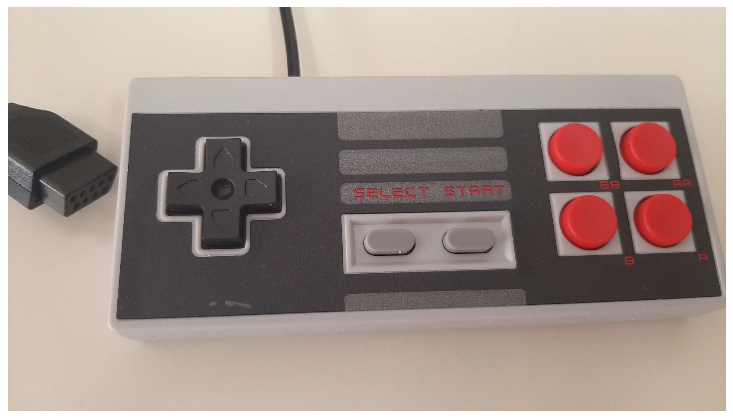
3.7. Joysticks
A joystick is the preferred input to play games. In the 1980s there were two types of joysticks: Kempston and Sinclair. Kempston joysticks had the switches (N, S, E, W, Fire) connected to an input port decoded at address 0x–1F while Sinclair joysticks were connected to the numeric keys on the keyboard. As finding original Kempston joysticks is very difficult, NES clones gamepads were used in this implementation. One can be seen in
Figure 4. These gamepads sent the state of the controller’s buttons in a serial synchronous interface. A component called “nes_gamepad” de-serialized the data and sent it to either the keyboard IP block or the Kempston interface IP block, depending on SW[17].
3.8. NIOS-II Co-Processor
The software running on the NIOS II processor was responsible for the support of the new features introduced in the system. It was developed in C and could be divided into three parts: SD interaction (SPI), Z80 Control, and File Access (FAT).
The SD interfacing was done using a FAT library called FatFs [
22] with an added interface for the NIOS II application to use. This library allowed the creation of files for save-state functionality, on top of the reading functionality many other FAT libraries have. The interface allowed listing the included files. A FAT library was used to read and write files from/to SD cards.
The Z80 Control consisted of two separate interfaces: one for DMA and one for the T80 to use as a peripheral.
3.8.1. DMA Interface
The DMA interface allowed the NIOS II to request memory access to the T80, to perform read/write operations on memory and I/O, and to stop the DMA, with or without the Non-Maskable-Interrupt-(NMI) signal enabled. It also allowed waiting, for n attempts, for the value in the CPU’s address bus to be higher than the end of screen RAM, 0x5800. The reason for this, and the NMI, is explained below.
3.8.2. NIOS II Control Interface
The peripheral interface was used to obtain the last sent command from the T80 and to clear the command register. A command register was used, called “nios_per_reg” in VHDL, due to the difference in clock speed between the NIOS and the T80. The register kept the command until NIOS finished it, resetting the register. Reads and writes to defined addresses worked as commands and not real read/write operations. These commands included:
a read to 0x17 was INIT, used to request that NIOS load the main menu into memory;
a write to 0x19 was STATE, requesting that NIOS save the contents of memory and the CPU’s registers to a snapshot file. A read to the same port was used by the T80 to notify NIOS that the register values were ready to be read;
a read to 0x19 was SD-related, used to request a list of 16 filenames of files inside the SD card;
a write to 0x19 was also SD-related, used to request the writing of the selected file’s contents into memory and the CPU’s registers;
4. Embedded Software
While part of the proposed methodology involved the interconnection of the NIOS II co-processor, it was also necessary to account for the embedded software on both CPUs, the Z80, and the NIOS II.
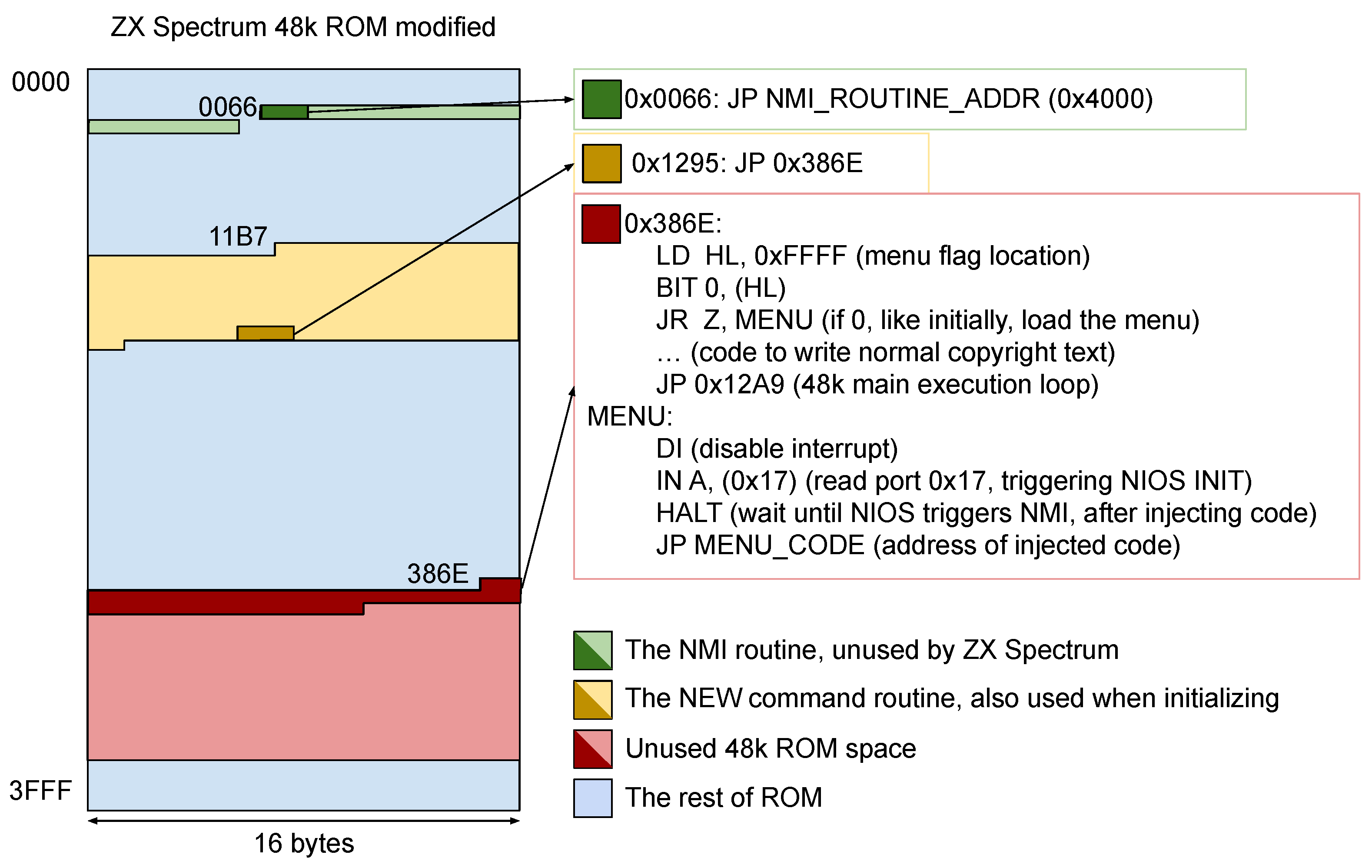
4.1. Modified ZX Spectrum 48K ROM
Even though it was intended to preserve as much as possible of the original system, including the ROM contents, it was necessary to introduce new code inside the ZX Spectrum 48K’s ROM on an unused region of ROM (0x386E). Moreover, to support the new start menu and the file selection menu, it was necessary to write them in RAM, as they would not fit the little free ROM. When the system boots up, instead of going straight to the basic console, it presents a menu with three choices: load a file from the SD card, go online (future work) or start the basic. The modified ZX Spectrum 48K ROM is illustrated in
Figure 5. Darker colors represent modified code, while brighter colors represent the regions described in the legend.
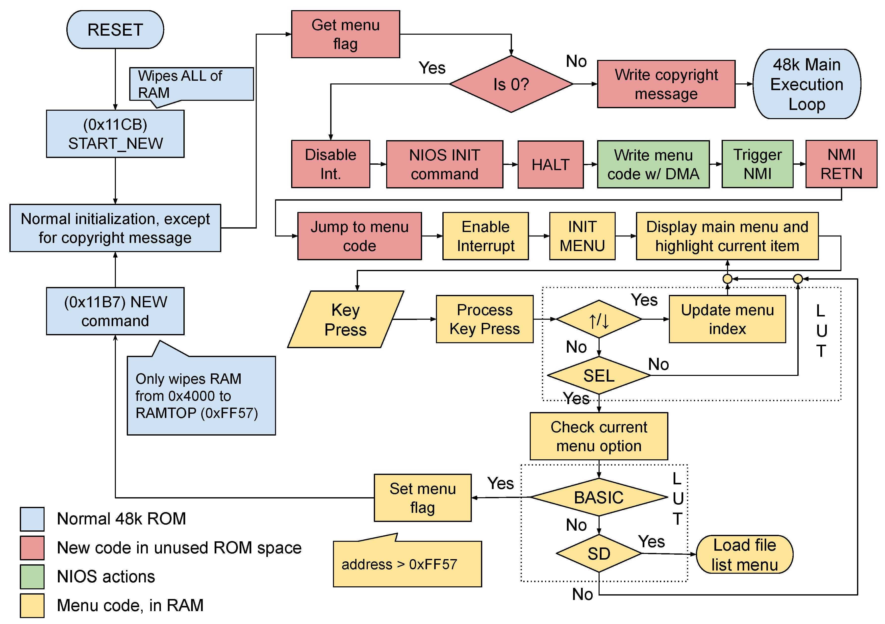
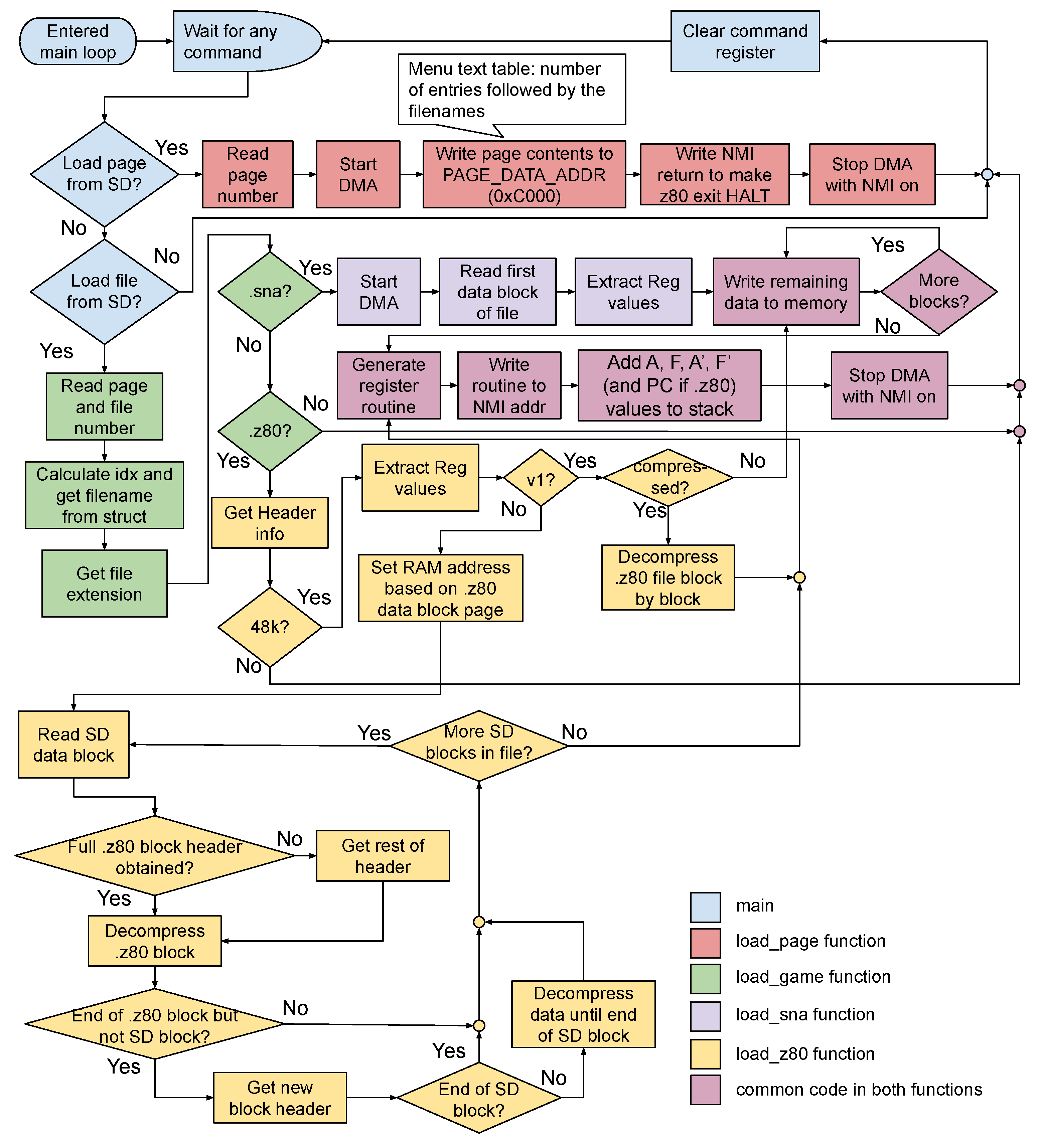
4.2. NIOS II Application
NIOS’ main contained a loop that checked the register for any command that had been sent, followed by the execution of that command. A flowchart representing this loop in its complexity is shown in
Figure 6. As the .z80 file format has multiple versions, these had to be considered for interpreting the files, as can be seen in
Figure 6.
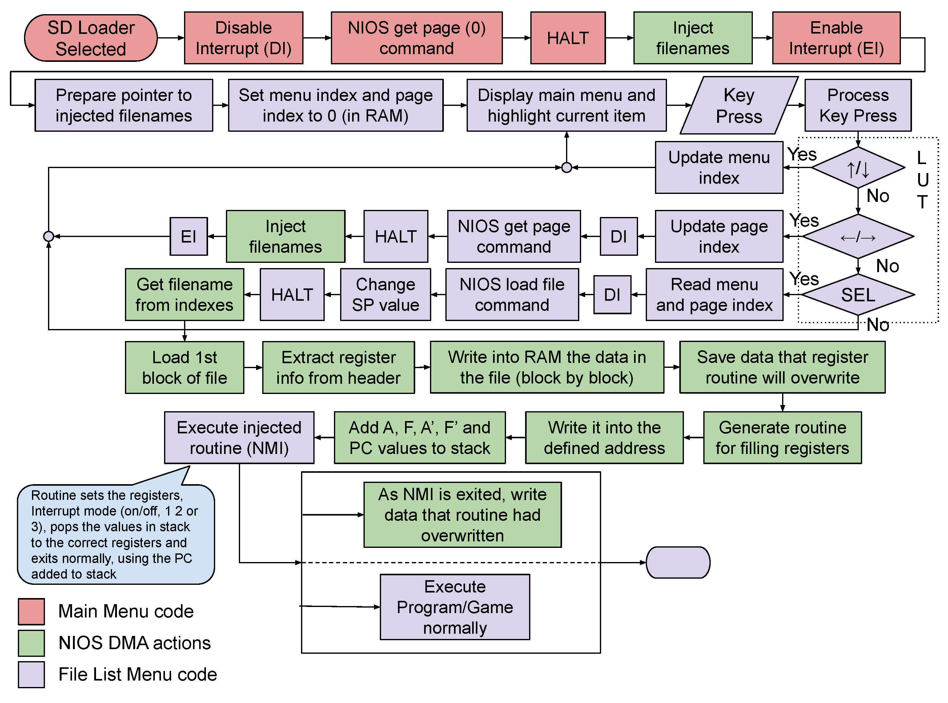
The new menus were created based on the ZX Spectrum 128K’s menus. A disassembly of ROM 0 of the 128 K was analyzed and the necessary routines were copied and adapted, to generate the menus used. Some routines were changed, to receive a parameter to differentiate the main menu from the file menu so that the full code of the menus could be compact without much repetition. The file menu obtained its data from a predetermined address that NIOS wrote the filenames to when the Z80 requested them, as the user selected the “SD Loader” option.
The menus used in the ZX Spectrum’s boot were written by NIOS during its initialization. The BASIC option in the menu jumped to the NEW routine in address 0x11B7, provoking a system reset. This made all of the RAM reset except for values below the address in the system variable RAMTOP (0xFF57). Therefore, the state of the menu flag was saved beyond this address, so that the reset did not overwrite it. The flag determined if the ZX Spectrum 48K code continued execution normally (1) or if it requested the menu from NIOS and executed it (0). By default, it was 0, as all of RAM was set to 0 during initialization, making the menu load, but selecting the BASIC option set it to 1 and resets.
A flowchart of the initialization of ZX Spectrum Fusion is in
Figure 7, where the main menu controls also reside. Interrupts were disabled before the HALT, to prevent the ULA from triggering them when it intended to trigger a jump to the keyboard scanning routine. The NMI input was still sampled when interrupts were disabled.
The file-list menu’s assembly-code flow, along with the process of loading a selected file, is shown in
Figure 8.
Without NIOS on, the T80 would remain halted forever, waiting for the NMI signal to execute a simple RETN instruction to leave the halted state after the menu was written.
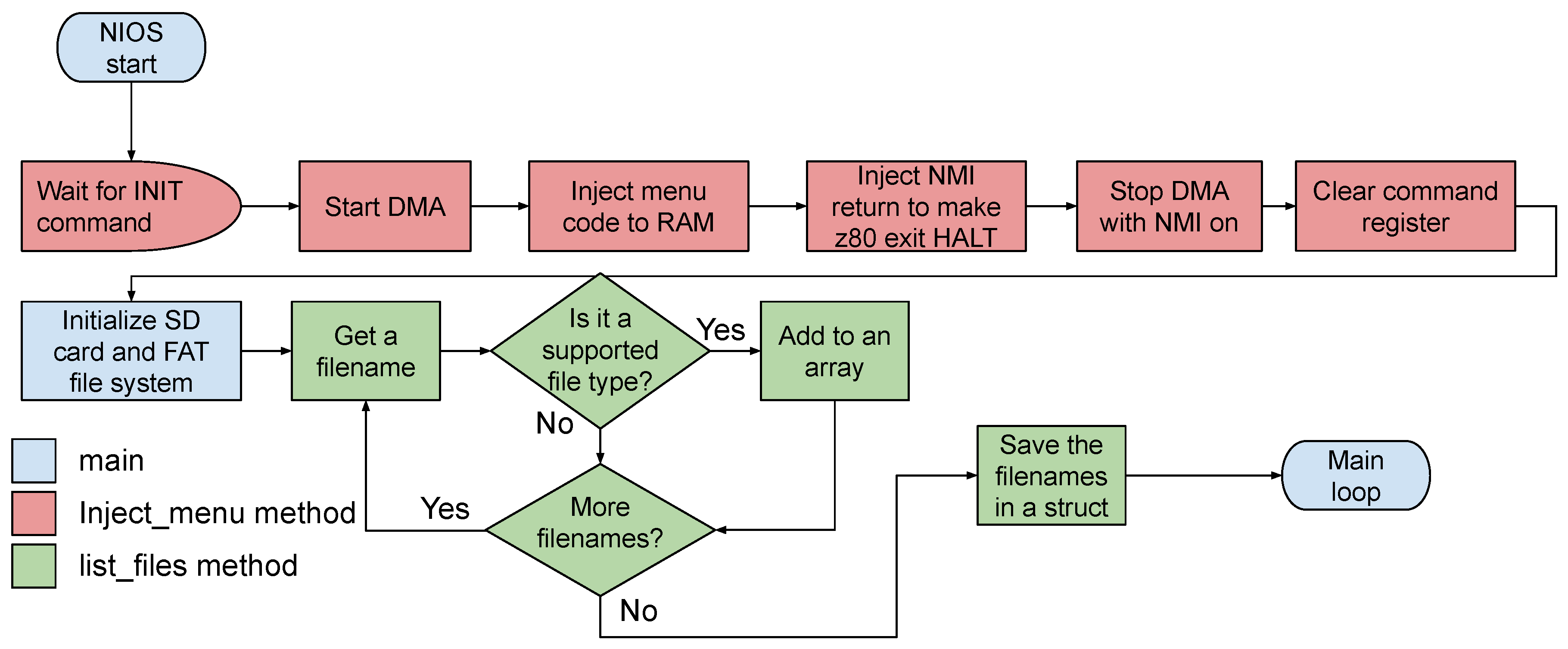
Figure 9 shows a flowchart of NIOS’ initialization.
4.3. File Reader
The file format reader opened the files and, depending on their extension (.z80 or .sna), decrypted them to write their contents into memory and the CPU’s registers. The file format reader used the SD-communication part of the software to open and read files. It also used the DMA interface to write the contents of the software into memory as it read them from the SD card, block by block.
When the Z80 CPU sent commands to the NIOS, it entered a HALT state, to allow time for NIOS to see the command and act on it. When the contents of a file were loaded to memory, a routine with the register values was generated for the Z80 to execute. This routine was loaded into the screen memory’s region, to avoid overwriting important program code. The values for the AF and AF’ regs were added to the stack, as these lacked direct load instructions, but had POP instructions. To avoid problems with the unknown location of the Stack Pointer (SP) before this operation, it was set as the bottom right of the screen region. After these writings, NIOS stopped the DMA with the Non-Maskable-Interrupt-(NMI) signal on. The unused NMI routine of the original ZX Spectrum, present in address 0x0066, was edited to perform a jump to the screen memory’s start, address 0x4000. In triggering the NMI, NIOS made the CPU execute the routine to load all the registers, including the PC to jump to when exiting the routine to execute the program.
The routines written in VRAM could cause visual effects in the corners of the screen. NIOS overwrote them with the original VRAM data by using the aforementioned function in the DMA interface. This function read the address the CPU was accessing, to check when it was no longer executing the routine in VRAM. It stays in a loop for n attempts until the condition was satisfied, and then the file format reader restored the video data, preventing the visual effect from staying on screen for more than half a second.
4.4. Save-State Functionality
Save-state functionality was added by using the same mechanisms as when a game is loaded. It was initialized via a push button on the target platform. This simulated a write to port 0x19 in the NIOS command register, starting the process. The screen memory was saved before being overwritten by a routine that wrote the contents of the registers in this same region. The Z80 then performed a read in port 0x19, to notify the NIOS of the register value’s availability. Certain values could not be obtained through assembly code. These included the state of the interrupts. Therefore, physical connections were created from the T80 to NIOS.
These register and interrupt information values were then written to the header of a new file with the name of the game loaded plus a suffix number. The previously saved screen data were written and then the rest of the data in RAM followed, completing the save-state file.
In the process of saving the registers to memory, these registers would lose their original values. Therefore, to resume the game accordingly, a load-registers routine was created, based on the saved register values, and the registers were brought back through an NMI.
The output was in the .SNA format, chosen for its simplicity. The name of the save file consisted of the name of the loaded game with an underscore and a two-digit number appended to the end. If no file was originally loaded through the SD Loader, the file was simply called “save_xx.SNA”, where xx represented the number. The save-state process required a couple of seconds to complete. To load the generated state, the user needed only to load it like a normal snapshot in the SD Loader menu.
5. Experimental Results
To validate that the proposed methodology worked as intended, several tests were made on ZX Fusion and its components.
5.1. Video
It started with the stand-alone testing of the video component, with a preloaded VRAM. It was observable that the image was displayed correctly.
Figure 10 shows testbench signals of the video component, where the video data were obtained in one flank of the clock and displayed in the next.
5.2. CPU and Memory
The T80 implementation was tested in a project where the target platform’s switches were used to input data and, therefore, instructions. The machine code of some of the instructions was loaded manually via the switches. The tested instruction included a data read from memory, an addition (modify), and a write back to memory. The test was a success, so the T80 was added to a project with BRAMs and the video component. At first, a small Z80 assembly routine was loaded into ROM that wrote an X in the corner of the screen. This worked successfully, so an original ZX Spectrum 48K ROM was loaded and the VGA screen showed the starting ZX Spectrum screen with the copyright message below.
5.3. PS/2 Keyboard
The new PS/2 keyboard component was implemented and tested on a stand-alone hardware project. In this project, the CPU address (keyboard half-row multiplexer) was determined by the FPGA board’s switches, and the LEDs on the board showed the 5-bit output data of the keyboard. The module successfully outputted the correct data values, depending on the address selected and the keys being pressed. The module was then added to the project with the T80, video component, and ULA IP Block. The ULA had to be added, as it was responsible for triggering the interrupts that scanned the keyboard. With these components set, the 48K’s ROM was loaded and the keyboard was tested in the BASIC editor. It was working correctly.
5.4. ULA
The internal counters of the ULA were implemented, based on Chris Smith’s book [
4]. However, the timings were tested, to make sure the implementation was successful. A quick Z80 assembly code was written that accessed the contended memory region in a loop. The Z80 and ULA’s signals were checked through ModelSim, and the clock could be seen being held high at the appropriate timings, based on diagrams in the aforementioned book [
4].
5.5. SD Card
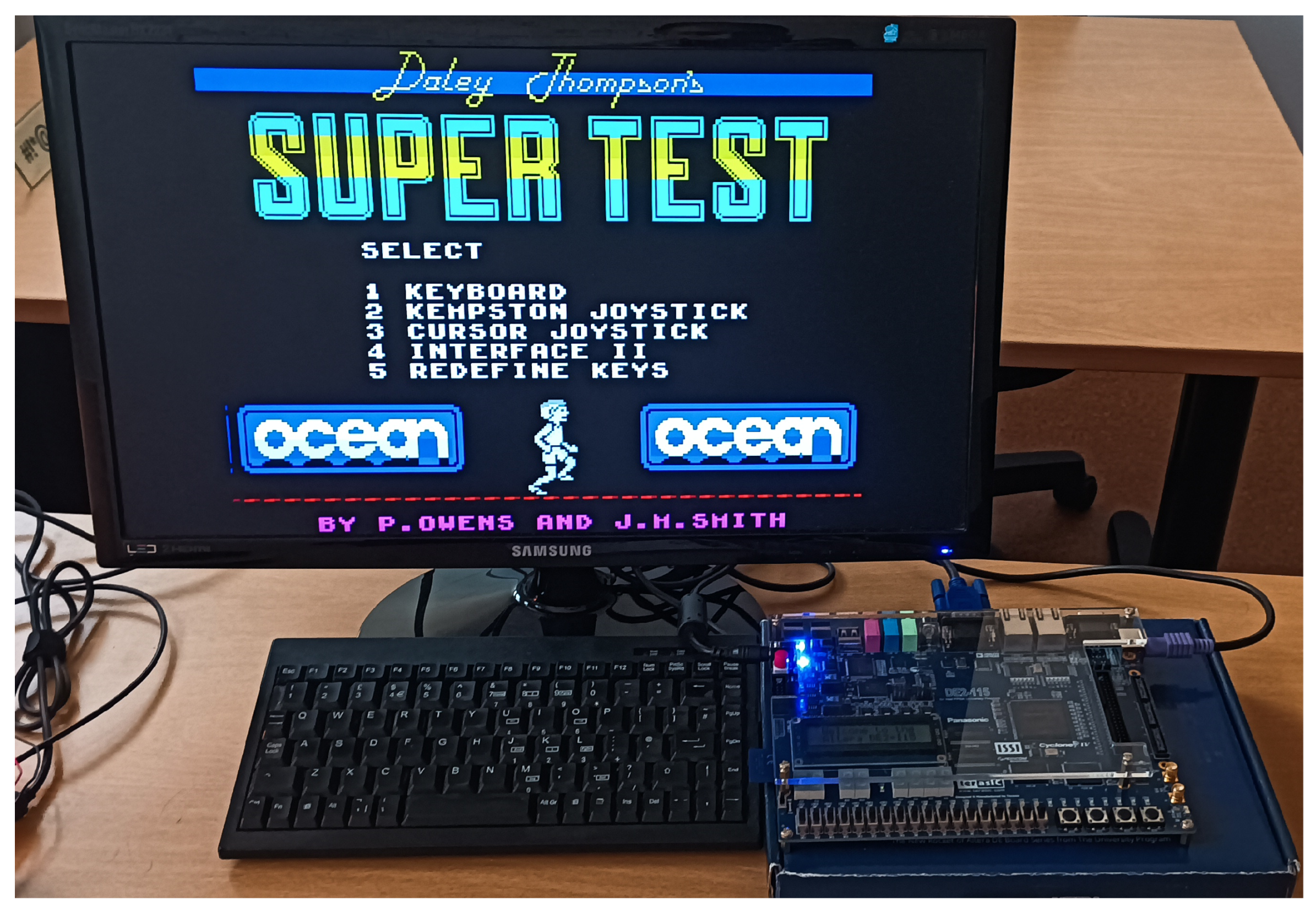
The SD card reading was tested by loading files of different formats, including versions, and different file name lengths. Moreover, the menu navigation was tested for the file selection. An SD card with a FAT32 file system and more than 16 files (29) was used to test the navigation, as each page could only list 16 files.
Figure 11 shows “Daley Thompson’s Super Test I” running in the implementation, after having been loaded from a file in the SD card. Game mechanics observable in original ZX Spectrum 48K computers were perserved.
5.6. Audio
A speaker was connected to the target platform’s audio output, to test the sound generator’s implementation. It was compared to online videos of the games being played, to confirm their accuracy. Audio input was tested by using an Android phone application called “ZX Tape Player”, to play audio-tape files. The ZX Spectrum successfully loaded multiple tape files.
Figure 12 shows “Bomb Jack II” running on ZX Fusion after having been loaded through the audio input. Every game loaded and ran as expected.
5.7. Gamepad
The NES gamepad controller was tested separately in a hardware project titled “nes_gamepad_test”. In it, the data being received were displayed in the board’s LEDs, where they were verified. The Sinclair-joystick interface was tested on the BASIC prompt, as these joysticks map to the keyboard numbers. The correct numbers were written with each input. The Kempston-joystick interface was tested with a small program written in BASIC. This program would read the 0x1F port of the Kempston interface and output a letter (N, R, L, D, U, F) based on the value being read corresponding to the pressed button (none, right, left, down, up, and fire). The correct letters always showed. In-game, the controllers worked as expected.
5.8. Save States
The generated files were tested for various games. These files correctly loaded the game in the state that it was in when the save-state process began. The games also resumed correctly after the save-state process. Save states on games loaded through audio input also worked correctly, being output as files with the name “save_xx.SNA”, as explained previously.
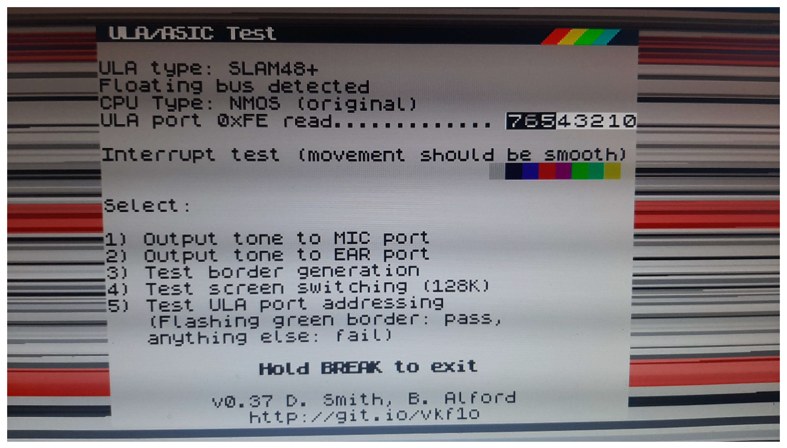
5.9. Test ROM
A separate ZX Spectrum Hardware Diagnostics ROM was used to evaluate the implemented system, based on how the test identified it. The project associated with the ROM is called “zx-diagnostics” by Rendanalford on GitHub [
23]. The ULA was detected as a SLAM48+ despite being implemented as an Issue 3 ULA. This may have been due to the implemented ULA’s timings being similar to the detected type of ULA. The test page can be seen in
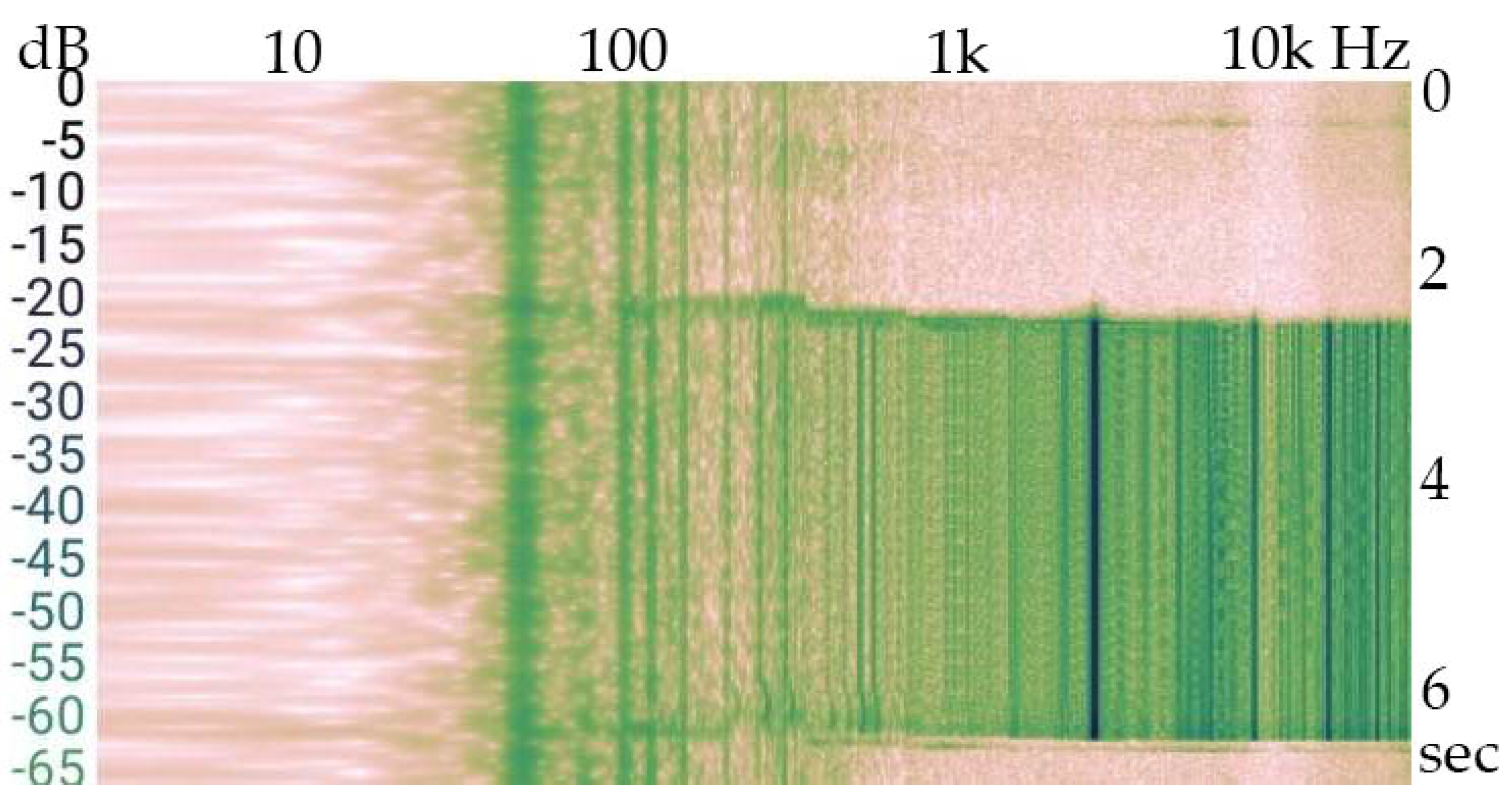
Figure 13. The other tests contained in this screen were successful, such as the EAR tone when the number 2 was pressed, which can be seen in
Figure 14.
6. Conclusions and Future Work
This work presents a novel method by which to interface with old computing systems so that they can use modern peripherals and features while remaining fully compliant with their original applications. The various tests done to ZX Fusion verified the methodology’s success, as the system was fully operational. To demonstrate its effectiveness an FPGA implementation of a ZX Spectrum 48K was created. Unlike most studied projects, this project supports snapshot file loading, extra keys on PS/2 keyboards, and save-state functionality. Other computing systems could also benefit from this work. In the future, the ZX Spectrum 128K could be implemented by adding memory paging to the design and the menu options of this implementation to the 128K’s menu. More features could be implemented, such as internet access. Internet access could allow users to obtain the snapshot files from websites and have them downloaded and loaded directly into the implementation. The bill of materials for this project is present in
Appendix A.
Author Contributions
Conceptualization, G.J. and R.P.D.; Methodology, G.J. and R.P.D.; Software, G.J.; Investigation, G.J.; Resources, R.P.D.; Writing—original draft, G.J. and R.P.D.; Writing—review & editing, G.J.; Visualization, G.J.; Supervision, R.P.D.; Project administration, R.P.D. All authors have read and agreed to the published version of the manuscript.
Funding
This work was supported by national funds through FCT, Fundação para a Ciência e a Tecnologia, under project UIDB/50021/2020 (DOI:10.54499/UIDB/50021/2020).
Data Availability Statement
The complete source code for the modernized ZX Spectrum project is publicly available on GitHub
https://github.com/A46006/ZX-Fusion (accessed on 15 January 2024) as an open-source project, under MIT license.
Conflicts of Interest
The authors declare no conflicts of interest.
Appendix A. Bill of Materials
The proposed ZX Spectrum system was constructed and can be reproduced using the following components:
DE2-115 FPGA board from Terasic − €423 (academic w/o import tax);
IO Expansion PCB for gamepad and ZX Spectrum+ keyboard − €5 (GERBER files on the project’s Github repository);
2× NES gamepad with DB9 connector − €9;
2× IDC10 to DB9 flatcable adapter − €4;
2× IDC10 (2 × 5 pin) male connectors for PCB − €1.
References
- McConnel, S. Z80: The Most Prolific CPU of All Time. 2016. Available online: https://www.kmuw.org/your-move/2016-03-10/z80-the-most-prolific-cpu-of-all-time (accessed on 22 December 2023).
- Zilog. Z80 Family, CPU User’s Manual; Zilog: Milpitas, CA, USA, 2004. [Google Scholar]
- Bee, H. Introduction to Gate Array. Available online: https://hardwarebee.com/introduction-to-gate-array/ (accessed on 3 August 2023).
- Smith, C. The ZX Spectrum ULA: How to Design a Microcomputer; ZX Design Retro Computer, ZX Design and Media: Sacramento, CA, USA, 2010. [Google Scholar]
- Beltfield, D. Screen Memory Layout. Available online: http://www.breakintoprogram.co.uk/hardware/computers/zx-spectrum/screen-memory-layout (accessed on 4 August 2023).
- Owen, C. IN and OUT. 1995. Available online: https://worldofspectrum.org/ZXBasicManual/zxmanchap23.html (accessed on 30 September 2023).
- What Is an FPGA? Available online: https://www.arm.com/glossary/fpga (accessed on 5 August 2023).
- Altera. Altera DE2-115 Development and Education Board—Specifications. Available online: https://www.terasic.com.tw/cgi-bin/page/archive.pl?Language=English&CategoryNo=139&No=502&PartNo=2#contents (accessed on 22 December 2023).
- Corporation, Altera. Cyclone IV Device Handbook; Altera Corporation: San Jose, CA, USA, 2009; Volume 1. [Google Scholar]
- Westcott, M. The Speccy2010: A Complete Guide for Non-Russian-Speakers. 2011. Available online: https://web.archive.org/web/20170706104143/http://matt.west.co.tt/spectrum/speccy2010/ (accessed on 6 September 2023).
- Stirling, M. Sinclair ZX Spectrum 48K and 128K on an Altera DE1 FPGA Board. 2016. Available online: https://github.com/mikestir/fpga-spectrum (accessed on 30 September 2023).
- ZX-Uno [ZX Spectrum Computer Clone Based on FPGA]. 2013. Available online: https://zxuno.speccy.org/maquina_e.shtml (accessed on 6 September 2023).
- Devic, G. A-Z80 CPU. 2014. Available online: https://opencores.org/projects/a-z80 (accessed on 6 September 2023).
- Rodriguez Jodar, M.A. ULA Chip for ZX Spectrum. 2012. Available online: https://opencores.org/projects/zx_ula (accessed on 6 September 2023).
- About-ZX SPECTRUM NEXT. 2017. Available online: https://www.specnext.com/about/ (accessed on 6 September 2023).
- ReVerSE-U16. 2019. Available online: https://github.com/mvvproject/ReVerSE-U16 (accessed on 6 September 2023).
- Nios Soft Processor Series. 2016. Available online: https://www.intel.com/content/www/us/en/products/details/fpga/nios-processor.html (accessed on 20 December 2023).
- Wallner, D.M. T80 CPU. 2002. Available online: https://opencores.org/projects/t80 (accessed on 6 September 2023).
- Larson, S. VGA Controller (VHDL). 2021. Available online: https://forum.digikey.com/t/vga-controller-vhdl/12794 (accessed on 27 September 2023).
- University of Toronto. EECG PS/2 Controller. 2023. Available online: https://www.eecg.utoronto.ca/~jayar/ece241_08F/AudioVideoCores/ps2/ps2.html (accessed on 2 July 2023).
- Wolfson Microelectronics. Portable Internet Audio CODEC with Headphone Driver and Programmable Sample Rates; Rev. 4.9; Wolfson Microelectronics: Edinburgh, Scotland, 2012. [Google Scholar]
- ChaN. FatFs—Generic FAT Filesystem Module. 2022. Available online: http://elm-chan.org/fsw/ff/ (accessed on 22 December 2023).
- Brendanalford. Brendanalford/zx-Diagnostics. Available online: https://github.com/brendanalford/zx-diagnostics (accessed on 1 September 2023).
| Disclaimer/Publisher’s Note: The statements, opinions and data contained in all publications are solely those of the individual author(s) and contributor(s) and not of MDPI and/or the editor(s). MDPI and/or the editor(s) disclaim responsibility for any injury to people or property resulting from any ideas, methods, instructions or products referred to in the content. |
© 2024 by the authors. Licensee MDPI, Basel, Switzerland. This article is an open access article distributed under the terms and conditions of the Creative Commons Attribution (CC BY) license (https://creativecommons.org/licenses/by/4.0/).


