Article

Dead-Time Effect in Inverters on Wireless Power Transfer

1
Faculty of Technical Sciences, Department of Power, Electronic and Telecommunication Engineering, University of Novi Sad, Trg Dositeja Obradovića 6, 21000 Novi Sad, Serbia
2
Faculty of Sciences, Department of Physics, University of Novi Sad, Trg Dositeja Obradovića 6, 21000 Novi Sad, Serbia
3
Institute of Information Technology, University of Dunaujvaros, Tancsics M. Str. 1/A, H-2401 Dunaujvaros, Hungary
4
John von Neumann Faculty of Informatics, University of Obuda, Becsi Str. 96/B, H-1034 Budapest, Hungary
5
Symbolic Methods in Material Analysis and Tomography Research Group, Faculty of Engineering and Information Technology, University of Pecs, Boszorkany Str. 6, H-7624 Pecs, Hungary
6
Faculty of Engineering and Information Technology, University of Pecs, Boszorkany Str. 2, H-7624 Pecs, Hungary
7
Cellular Bioimpedance Research Group, Szentagothai Research Centre, University of Pecs, Ifjusag Str. 20, H-7624 Pecs, Hungary
*
Author to whom correspondence should be addressed.
Electronics 2024, 13(2), 304; https://doi.org/10.3390/electronics13020304
Submission received: 4 December 2023 / Revised: 28 December 2023 / Accepted: 2 January 2024 / Published: 10 January 2024

Abstract

:
This paper presents a comprehensive analysis of the dead-time effects in wireless power transfer systems based on LCC-S topology. In these systems operating at high frequencies, the ratio of dead-time versus the operating period becomes critical, and the dead-time issue can cause certain problems regarding power quality, efficiency, and output voltage ripple. The impact of input quantities such as voltage and switching frequency on the efficiency and output power of the LCC-S-tuned WPT system was also investigated. The optimal combination of these parameters used to achieve the maximum efficiency for a target output power and to set the appropriate value of the dead time were determined by running multiple simulations using the MATLAB R2023b software platform. It was also shown that the output voltage remained unchanged with and without a load and up to 1200 ns of dead-time, which provides a simple implementation of the corresponding mathematical model. In the recommended interval of 600–1500 ns, the influence of the dead-time on the value of the output voltage amplitude is less than 10%. The validity of the proposed method was confirmed through the implementation of the experimental prototype, a 5 kW wireless power transmission system, and the obtained results were in accordance with the simulation results.

1. Introduction

In recent decades, wireless power transfer (WPT) technology has experienced significant progress, offering a convenient and efficient means of transferring electrical energy without physical connections. This technology has found applications in various areas, including electric vehicles, mobile devices, medical devices, and home electronic appliances. Using WPT technology eliminates the need for physical cables and connectors. The power from the charging pad on the ground (or other surfaces) sent to a receiver unit installed on the vehicle is transferred via an electromagnetic field. Therefore, drivers do not need to physically plug in the vehicle when the WPT is applied, which is a great convenience. WPT technology can support high-power charging, making it possible to recharge an electrical vehicle relatively quickly. This technology continues to be developed, with the goal of matching or exceed the charging speeds of traditional plug-in methods. WPT does not require a physical charging station at each parking spot. Instead, charging pads can be embedded in roads, parking lots, or other surfaces, providing more flexibility in deploying charging infrastructure. WPT standards like SAE J2954 are emerging, promoting compatibility among different vehicle brands and charging infrastructure providers. WPT systems are designed with safety features, such as automatic shutdown if foreign objects are detected on the charging pad, in order to ensure safety during the charging process.
Many studies have been conducted in this field, including power management [1], magnetic material design [2], coil optimization [3,4], etc. In separate studies [5,6], the WPT for IoT applications and the use of arrays to transfer power to freely moving objects were analyzed in detail.
In WPT systems, the inverter has a key role in converting direct current (DC) power into high-frequency alternating current (AC) power, which is then transmitted wirelessly. A typical inverter with insulated-gate bipolar transistor (IGBT) technology in a WPT system, which is crucial for the conversion of DC current to AC current for efficient wireless energy transmission, is described in refs [7,8,9]. The IGBTs are commonly used in power electronics due to their ability to handle high voltage and current levels. In a WPT inverter, IGBTs are employed, considering their switching capabilities and durability. Their primary function is to convert the incoming direct current into an alternating current, as this conversion is necessary for compatibility with the resonant circuit used in WPT systems. The inverter modulates the DC voltage to create a sinusoidal AC waveform that matches the resonant frequency of the system. The inverter with IGBTs is controlled with a microcontroller. These controllers generate the required switching signals for the IGBTs to regulate the output voltage and the frequency precisely. Advanced control algorithms are used to maintain optimal power transfer efficiency and to adapt to variable load conditions [7,9,10]. WPT systems often operate at high frequencies, typically in the range of tens to hundreds of kHz. The IGBTs switch at these frequencies, and they are capable of handling the rapid switching required for efficient power transfer.
During their operation, IGBTs can generate heat, especially at high power levels. Therefore, appropriate cooling mechanisms such as heatsinks or fans are required, which have been designed and integrated into inverters. Their role is to dissipate the heat, and thus to maintain regular working conditions.
During inverter design, particular attention is paid to the dead-time issue. Dead-time in two-phase inverters with IGBTs represents a crucial concept in power electronics control to prevent destructive and inefficient shoot-through currents [11]. In a two-phase inverter, there are typically two legs, each consisting of two IGBTs (high-side and low-side) that control the flow of current through a load. The dead-time refers to the intentional delay between turning off one IGBT in a phase leg and turning on its complementary IGBT. However, such a blanking period can affect the reliability, power quality, and losses of the system [11,12,13,14,15,16,17,18]. Furthermore, if issues associated with dead-time are not addressed appropriately, it may result in voltage distortions [11]. Additionally, switching losses can occur due to voltage polarity reversal [12]. The dead-time may cause issues related to phase errors, affecting the transmitted power. To minimize the dead-time effect, regulation methods based on buck converters have been proposed [11]. Still, these methods cannot completely eliminate the dead-time effect [12,13]. Compensation methods require precise current detection and a complex algorithm, while their performance is highly dependent on the system parameters [12,13]. The dead-time issues in WPT systems have been reported in ref. [15]. In refs [8,16], the dead-time effect in a WPT system is discussed briefly, and a control strategy is implemented on the dual-active bridge circuit to eliminate the effects of the dead-time.
Considering all these facts [19,20,21,22,23,24,25,26,27,28], this paper presents a detailed theoretical analysis and experimental verification of the dead-time effect on a WPT system in an inverter. The main goal of this research is finding the optimal dead-time value in order to provide the maximum power transmission by reducing the losses and voltage distortion. This study was carried out to analyze the influence of dead-time on changes in amplitude and first voltage harmonics at the output of the inverter. This analysis is significant for the implementation of a specific mathematical model such as the charging of batteries when the output voltage changes.
The main contribution of this research to the literature data is reflected in the results related to the invariance of the output voltage, with and without a load, up to a dead-time value of 1200 ns. In the recommended interval of 600–1500 ns, the influence of the dead-time on the value of the output voltage amplitude is less than 10%, as will be shown in this paper.
This paper is organized as follows: the Introduction is followed by an analysis of the theoretical background of the dead-time issue and operational waveforms of a WPT system in Section 2. Section 3 presents am analysis of the resonant compensation network. The dead-time effects of the WPT systems in the experiments are shown in Section 4. Finally, the conclusion is presented in Section 5.

2. Dead-Time Effects of One Active Bridge WPT System

As it was mentioned, in WPT systems operating at high frequencies, the ratio of dead-time versus the operating period becomes more prominent, since the dead-time effect can cause several difficulties [29,30]. Some of these difficulties are listed below [31,32]:
  • Efficiency—The dead-time affects the overall efficiency of the WPT system. If the dead-time is too short or too long, it can lead to increased power losses. A short dead-time may cause shoot-through current and increase switching losses, while a long dead-time can result in decreased power transfer efficiency due to extended periods of no power transfer [21,22].
  • Power quality—The dead-time can influence the output waveform quality of the inverter. Improper dead-time management may lead to distorted voltage and current waveforms, which can affect the power factor and harmonic content of the system [23].
  • Output voltage ripple—The dead-time can also contribute to the output voltage ripple. If the dead-time is not properly optimized, it may introduce voltage fluctuations in the output, thus affecting the stability of the WPT system [24].
  • Electromagnetic interference (EMI)—Poorly managed dead-time can increase the electromagnetic interference emissions, which may interfere with other electronic devices and lead to compliance issues with electromagnetic compatibility (EMC) standards.
  • Switch stress—Incorrect dead-time settings can subject these switches to higher stresses, potentially reducing their reliability and lifespan.
  • Control complexity—Dead-time management requires precise control algorithms and sensing techniques. Implementing and tuning these control systems can add complexity to the overall design of the WPT system.

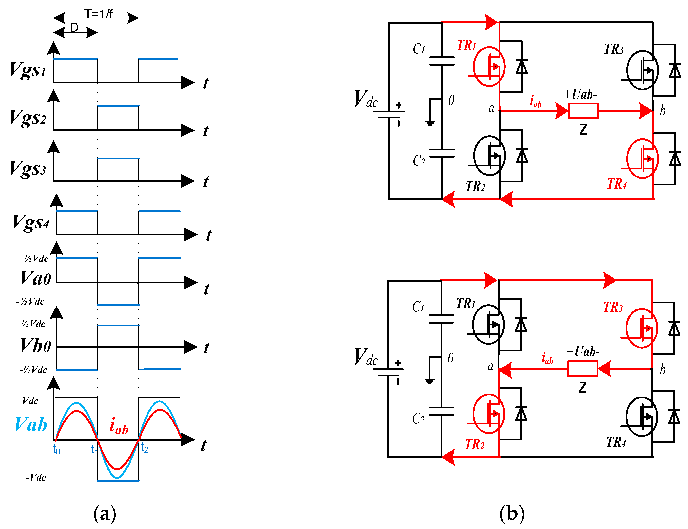
2.1. Switching Characteristics without the Dead-Time Effect

In this work, in two-phase inverters with IGBTs, the dead-time is considered as a mandatory parameter in order to prevent destructive and inefficient shoot-through currents [21].
Figure 1 shows the ideal switching characteristics (a) and the equivalent circuit operation (b) of two-phase inverters with IGBTs without dead-time. Cross-conduction occurs when the high-side and low-side IGBTs in the phase leg are turned on simultaneously. This results in a short circuit across the DC bus, causing excessive current flow, increased power losses, and potential damage to the IGBTs. However, this setup will be explained in further text as a part of the theoretical discussion in general.
The waveform Vgs1-Vgs4 shows the gate pulses of the appropriate IGBT MOSFET switches TR1–TR4,, while the quantities Va0, Vb0 indicate the voltages in points a and b. This setup presents the phase-legs inverter. The Vab is the fundamental component of the sine wave of the inverter output voltage, while the Iab is the sine current through the load impedance Z.
In this case, there are two operating modes: Mode A and Mode B:
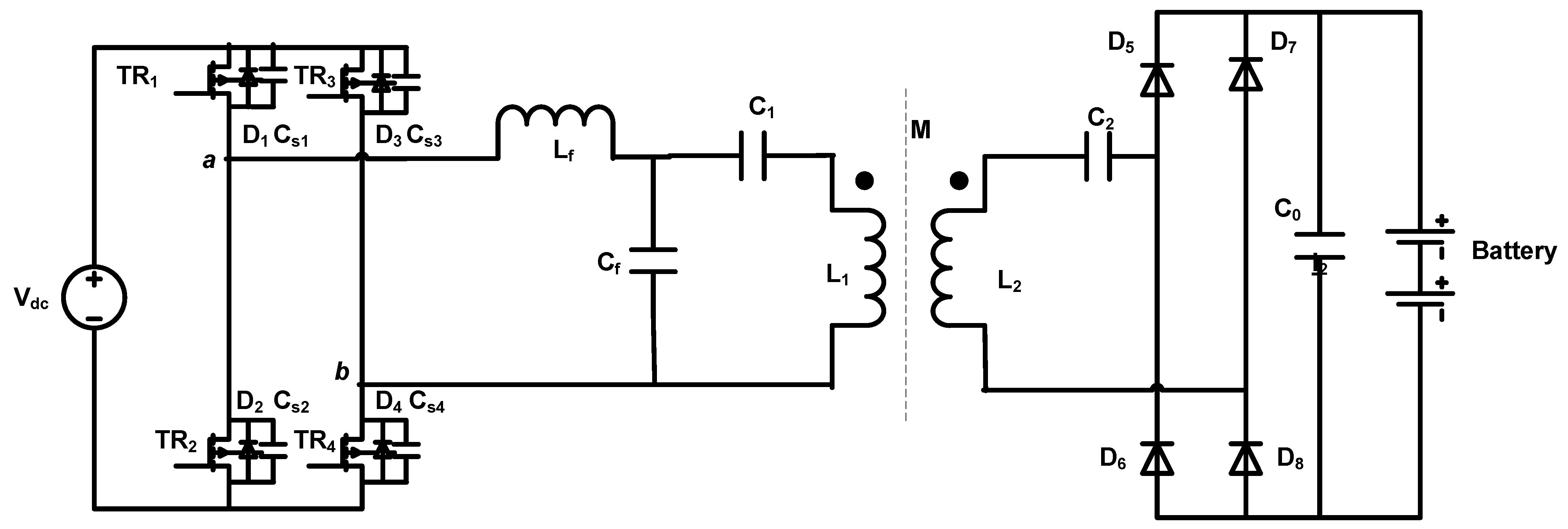
  • Mode A is applied to the interval from t0 to t1: TR1 and TR4 are ON, TR2 and TR3 are OFF. The sine wave current is positive and flows through TR1 and TR4. The output voltage Vab is a positive load +VDC because Va0 is VIN/2 and Vb0 is −VIN/2. The difference between Vao and Vbo is VIN.
  • Mode B is applied to interval from t1 to t2: TR1 and TR4 are OFF, TR2 and TR3 are ON. The sine wave current is negative and flows through TR2 and TR3. The output voltage Vab is a negative load −VDC because Va0 is −VIN/2 and Vb0 is +VIN/2. The difference between Vao and Vbo is −VIN.

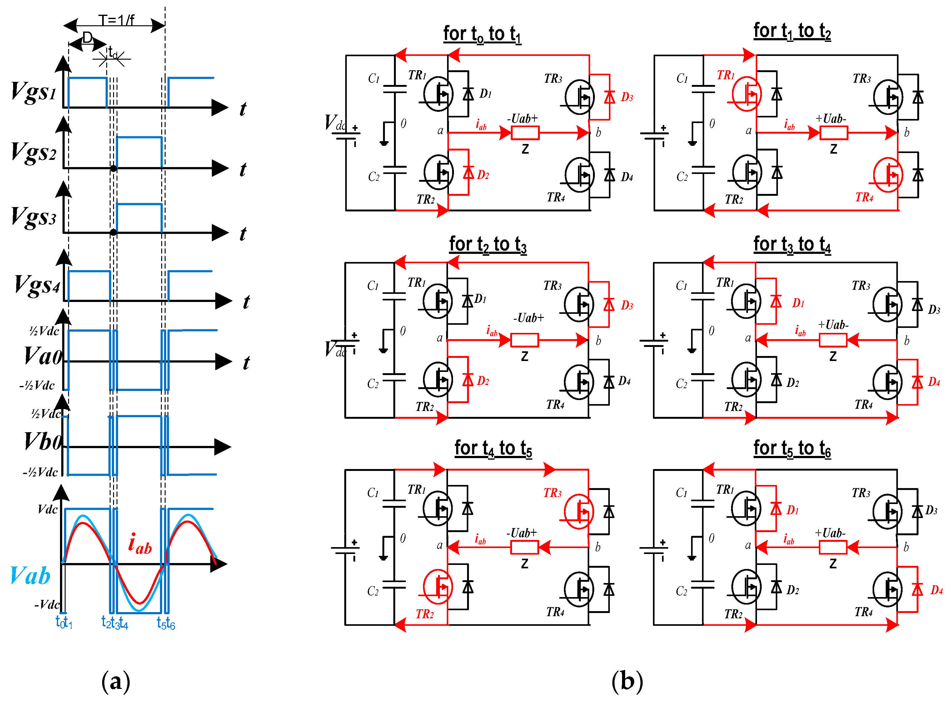
2.2. Switching Characteristics with the Dead-Time Effect

Figure 2 shows the switching characteristics (a) and the equivalent circuit operation (b) of the two-phase inverters with IGBTs dead-time. Parameter td refers to the dead-time interval between the complementary switching instances of the inverter.
During the dead-time, both the IGBTs in the inverter phase-leg are OFF, and the current flows through the IGBT body-diodes. If the current changes polarity during the dead-time, the pole voltages change polarities. The generation of a signal will be explained in terms of time modes (following order t1-t2, t2-t3, t3-t4, t4-t5, t5-t6, t0-t1), as shown in Figure 2b:
  • Mode 2: From t1 to t2 → Transistors TR1 and TR4 are turned ON and TR2 and TR3 are turned OFF, and the current iab flows from point a to point b, since the voltage at point a is positive and equal to Vdc/2, while at point b, it is negative and equal to −Vdc/2. In this case, the output voltage Vab = Vdc.
  • Mode 3: From t2 to t3 → All transistors are turned OFF. This is the effect of dead-time. The direction of the current iab remains the same as in mode 2. The current iab flows through the anti-parallel diodes D2 and D3; therefore, the voltage at point b is Vdc/2, whereas the voltage at point a is −Vdc/2. Hence, the voltage at the output is Vab =Vdc.
  • Mode 4: From t3 to t4 → All transistors are turned OFF. The current iab flows through the anti-parallel diodes D1 and D4 in the direction from point b to point a. The voltage at point b reached Vdc/2, and the voltage at point a reached −Vdc/2; thus, the output voltage is Vab= Vdc.
  • Mode 5: From t4 to t5 → The transistors TR3 and TR2 are turned ON. The current iab flows from point b to point a, the voltage at point a is −Vdc/2, and at point b is + Vdc/2. Hence, the output voltage is Vab = −Vdc.
  • Mode 6: From t5 to t6 →All transistors are turned OFF. This is the effect of the dead-time. The inductor current iab cannot change its direction; thus, it remains the same as in mode 5, and the diodes D1 and D4 conduct. The voltage pole of point a is positive + Vdc 2, while the pole of point b is negative −Vdc/2; thus, the output voltage is Vab = Vdc.
  • Mode 1: From t0 to t1 → All transistors are turned OFF. The current iab flows through the anti-parallel diodes D2 and D3. The voltages at points a and b are −Vdc/2 and +Vdc/2, respectively. Therefore, the output voltage across the load is Vab =Vdc.
Therefore, the dead-time in two-phase inverters with IGBTs is a critical component of inverter control strategies to ensure safe and efficient operation while minimizing waveform distortion and losses. However, dead-time in two-phase inverters can introduce significant challenges in achieving high efficiency and reliable power transfer. Deviations from rectangular pulses in voltage forms (Figure 2a) are the consequence of the dead time issue, and they influence the effective energy transfer. The next chapter addresses some of these challenges.

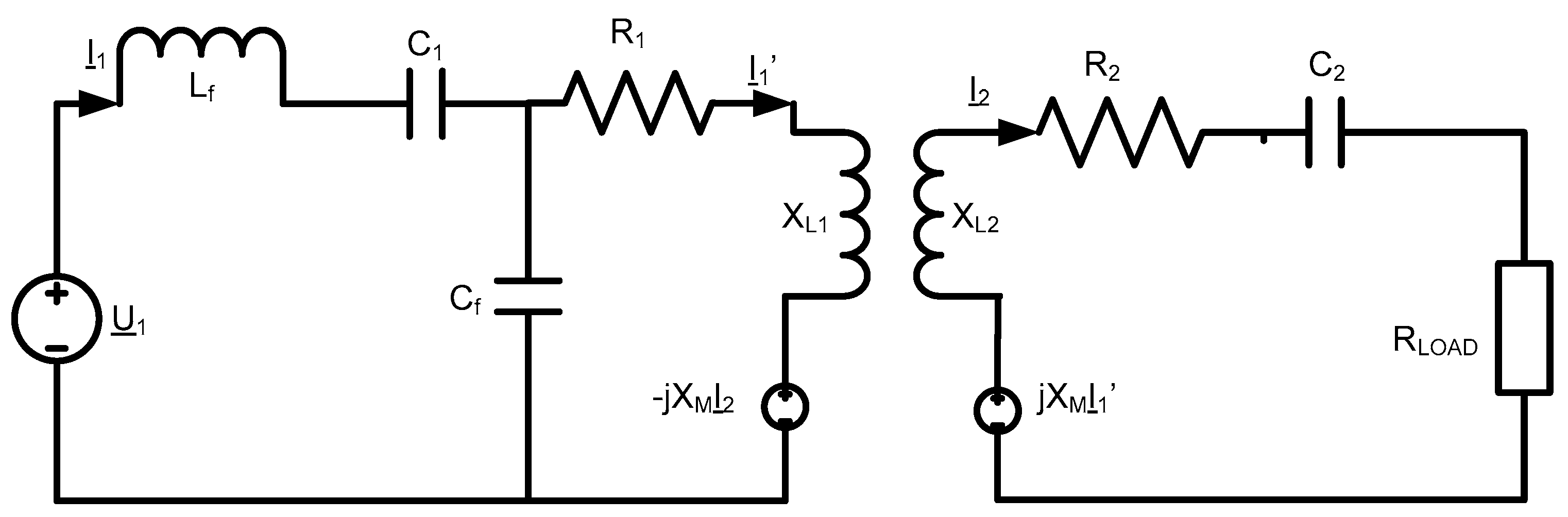
3. Modeling of WPT and System Analysis of Resonant Compensation Network

The configuration of the LCC-S resonant WPT system [4,7] is shown in Figure 3. The full-bridge inverter formed with four IGBTs (TR1–TR4) enables the DC input to be transformed into high-frequency AC power. The transmitting side consists of L1, Lf, Cf, and C1, where L1 represents the primary resonant tank. This tank is tuned to have the same resonant frequency as the switching frequency of the full-bridge inverter. The high frequency AC power resonates in the primary resonant tank. The receiving side contains elements L2 and C2, where L2 represents the secondary resonant tank. To receive the power from the primary side, this tank must match the switching frequency of the full-bridge inverter. The high-frequency AC power is transmitted wirelessly through the main coupling between the main coils L1 and L2, described with mutual coefficient inductance M. Afterwards, it is converted back to DC by the rectifier made of four diodes D5D8 and filtering capacitor C0.
The key properties of the LCC-S topology are:
  • Series compensation: Series compensation networks are added to reduce the voltage distortion caused by the dead-time. This enhancement improves the control over the output voltage waveform, resulting in increased power transfer efficiency.
  • Enhanced power quality: The LCC-S topology minimizes the harmonic generation and voltage distortion, ensuring that the output voltage complies with required power quality standards.
  • Improved resonant behavior: The series compensation enhances the resonant behavior of the system, optimizing the wireless power transfer efficiency at the resonant frequency.

3.1. Calculation of the Phase Regulation Parameters of the WPT System with an LCC-S Resonant Compensation Network

The working principle of the investigated WPT system with an LCC-S resonant compensation network with a load is completely based on the phase regulation. Therefore, the parameters of the phase regulation were calculated using the equivalent electrical circuit shown in Figure 4.
The resistances of the coils and capacitors in the transmitting (R1) and receiving part of the circuit (R2) are marked as R 1 = R C 1 + R L 1 and R 2 = R C 2 + R L 2 , respectively.
The equation that connects the currents I1 and I2 is given as:
I ̱ 1 = R 2 + R L o a d + j X L 2 X C 2 j X M I ̱ 2
Where XL2 is inductive reactance, XC2 is capacitive reactance, XM is mutual reactance, and RLoad is resistance of the load.
The parameters of the transmission coil part of the circuit in Figure 4 are calculated as follows:
j X C f I ̱ 1 I ̱ 1 = R 1 + j ( X L 1 X C 1 ) I ̱ 1 j X M I ̱ 2
and U1 is determined as:
U ̱ 1 = j ( X L f X C f ) I ̱ 1 + j X C f I ̱ 1 .
Quantities XL1 and XLf are inductive reactances, while XC1 and XCf are capacitive reactances. Using expressions (1) and (2), the following relations can be derived:
j X C f I ̱ 1 + j X M I ̱ 2 = R 1 + j ( X L 1 X C 1 X C f ) I ̱ 1
j X C f R 1 + j ( X L 1 X C 1 X C f ) I ̱ 1 + j X M R 1 + j ( X L 1 X C 1 X C f ) I ̱ 2 = R 2 + R L o a d + j X L 2 X C 2 j X M I ̱ 2
Based on expressions (4) and (5), the U1 and I1 are obtained as follows:
I ̱ 1 = R 1 + j ( X L 1 X C 1 X C f ) R 2 + R L o a d + j ( X L 2 X C 2 ) X M X C f + X M X C f I ̱ 2
U 1 = j X L f X C f + X C f 2 R 2 + R L o a d + j ( X L 2 X C 2 ) R 1 + j ( X L 1 X C 1 X C f ) R 2 + R L o a d + j ( X L 2 X C 2 ) X M 2 I 1
Using expressions (1), (6), and (7), the input impedance Z ̱ i n = U ̱ 1 I ̱ 1 can be expressed as:
Z i n 1 = X C f 2 R 1 + R L o a d R 1 + j ( X L 1 X C 1 X C f ) R 2 + R L o a d + j ( X L 2 X C 2 ) X M 2 + j X L f X C f + X C f 2 ( X L 2 X C 2 ) R 1 + j ( X L 1 X C 1 X C f ) R 2 + R L o a d + j ( X L 2 X C 2 ) X M 2
The inductors L1, L2, Lf and capacitors C1, C2 are chosen in a way to achieve the resonance:
X L 2 X C 2 = 0
X L 1 X C 1 X C f = 0
Finally, the ratio of the currents and the input impedance can be expressed as:
I ̱ 1 I ̱ 2 = 1 X C f R 1 R 2 + R L o a d + X M 2 X M
Z ̱ i n = X C f 2 ( R 2 + R L o a d ) R 1 R 2 + R L o a d + X M 2 + j ( X L f X C f )
The phase angle α is given as:
α = 2 arccos π 2 2 U 1 _ r m s U d c
In order to verify this comprehensive theoretical analysis, a simulation of the operation of a WPT with an LCC-S topology was performed.

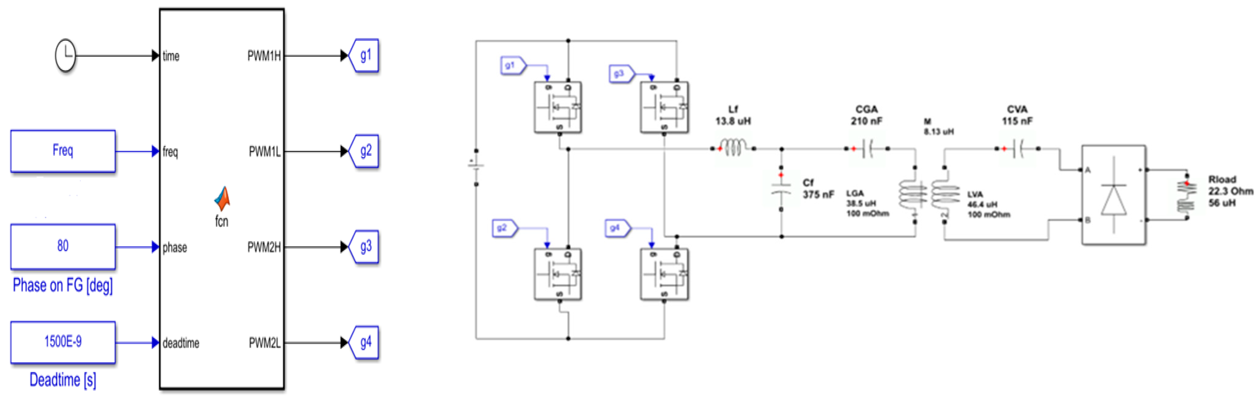
3.2. Analyzing a Wireless Power Transfer (WPT) System in MATLAB

One of the goals of the present study is to analyze and optimize the behavior of the investigated WPT system using simulations in MATLAB software. The theoretical model will be verified through simulations, and it will be used to obtain the parameters for the experimental setup.
The proposed model of a WPT system with an LCC-S resonant circuit is shown in Figure 5. The main component is the inverter, consisting of four IGBTs controlled in phase via four gates. The control block shown on the left side of Figure 5 is used for the frequency, phase, and dead-time setup. The model also includes a resonant compensation circuit (inductor Lf, capacitors Cf, CGA, and CVA), a transformer of transmission ratio of 1:1, a diode rectifier, and a resistive switching model.
The following quantities were selected: the input DC voltage is Uin = 310 V, the resonant frequency is f = 70 kHz, and the transfer gap is h = 100 mm. The parameters of the LCC-S resonant WPT system are listed in Table 1.
Two methods are used for the measurement of the mutual inductance:
  • Using an impedance analyzer, when the transmitter and receiver are connected to each other via one coil (so that the winding direction is the same), the total inductance is measured. Furthermore, based on the measured total inductance, the mutual inductance is obtained using the following expression:
    M = L t o t a l L _ G A L _ V A 2 .
  • The second method is applied before the induced EMS: The receiver is excited by a sinusoidal current of amplitude I and frequency f, and the amplitude of the induced voltage U is measured at the open transmitter. Based on these values, the mutual inductance is calculated as:
    M = U 2 π f I
Both methods gave the same result for the mutual inductance, which can be seen in Table 1 (M = 8.13 uH).
Figure 6 shows the inverter’s output voltage and current. Observing Figure 6a at the bottom of the diagram, several strange shapes as a short-lived peak in the voltage can be noticed. This phenomenon is a consequence of dead-time existence. Several papers provide a detailed analysis of this phenomenon [5,6,7,8], which is usual for the given settings.
Figure 7 shows the graph of the output voltage Uout in relation to the value of the dead-time. The red curve represents the output voltage with Rload, while the blue curve represents the output voltage without Rload. In both cases, the system behaves in a similar way. Namely, the output voltage remains unchanged with and without the load up to 1200 ns of dead-time, which is significant. This provides a simple implementation of the mathematical model. The behavior of voltage at higher dead time values is a direct consequence of the existence of dead-time. Therefore, the recommended interval of the dead-time is 600–1500 ns. A lower side time limit corresponds to the IGBT turn off time, and the upper side restriction is due to the change in amplitude behavior, which is less than 10%.
In the literature [24,25,26,29] related to a similar topic, the absence of an analysis of the output voltage behavior with and without a load as a function of the dead-time is revealed. This makes the conducted measurements significant.
The dead-time is typically implemented in the control algorithm of the inverter [27]. The microcontroller responsible or the inverter control calculates and enforces the appropriate dead-time delays based on the received switching commands. The amount of required dead-time can vary based on several factors such as the characteristics of the IGBTs, the voltage and current levels, and the desired switching frequency. To account for variations in the operating conditions, the dead-time is frequently and dynamically adjusted. While dead-time is necessary to prevent shoot-through, excessive dead-time can lead to increased switching losses and reduce the overall efficiency. Therefore, to maintain a high inverter efficiency, a compromise between ensuring adequate dead-time and minimizing its duration needs to be accomplished.
3.
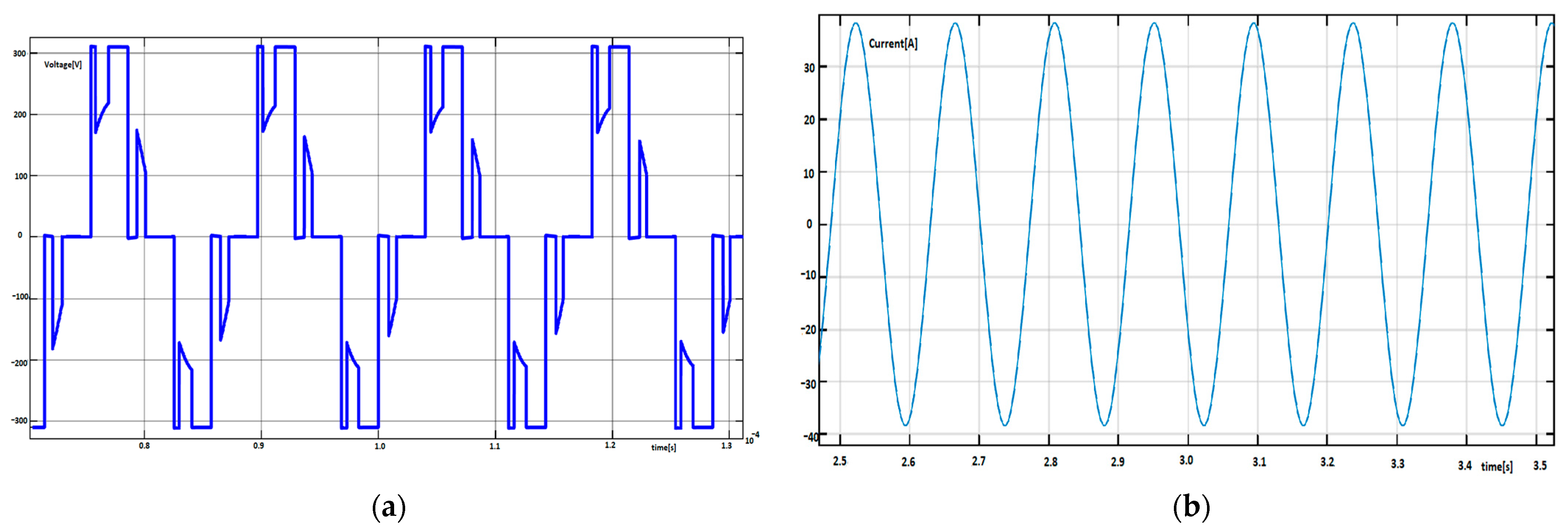
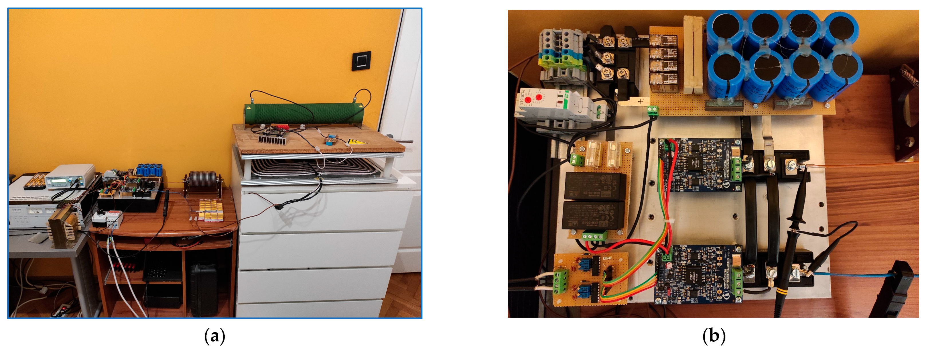
Experimental Results and Discussion
In order to obtain an appropriate value of the switching dead-time in the LCC-S resonant WPT system, an experimental prototype was realized. The LCC-S resonant circuit is a key element in this prototype. It consists of inductors and two capacitors on the transmitter side and of capacitors on the receiver sides. The LCC-S configuration helps in achieving efficient power transfer by minimizing losses and maximizing coupling between the transmitter and receiver.
The LCC resonant circuit operates at its resonant frequency, which is determined based on the values of the inductors and capacitors. Bringing the transmitter and receiver in close proximity ensures their tuning to the same resonant frequency. This ensures maximum energy transfer between the two sides of the circuit.
The theoretical model is verified through the simulations used for obtaining the parameters for the experimental setup. The inverter is designed to work in conjunction with the resonant network of the WPT system. It synchronizes its output frequency with the resonant frequency of 70 kHz to maximize the power transfer efficiency. The experimental platform, a prototype of a WPT system with an LCC-S resonant circuit, is shown in Figure 8a. This is an advanced wireless charging system that leverages resonant technology to efficiently transfer electrical power from a source (transmitter) to a device (receiver).
The transmitter unit is responsible for generating and transmitting the wireless power. It consists of the following elements shown in Figure 8b:
  • Three-phase bridge rectifier MDS150A1600V [33]: The rated current of this module is 150 A, and the maximum allowed working voltage is 1600 V.
  • Soft start circuit for capacitor charging in the DC circuit: When the inverter is switched on, the capacitors in the DC circuit are charged through resistors that limit the initial current (initial charge current) and thus protect the diode rectifier. After a certain time, the resistors are bridged. The delay is realized by a time relay. The capacitor charging resistors are 2 × 150 Ω/25 W, connected in parallel.
  • Capacitors in the DC circuit: The total capacity of the capacitors is 940 µF, and the breakdown voltage is 800 V. In the DC circuit, the resistors are placed, and they provide the discharge of the capacitor after the inverter is turned off. The total resistance value is 22 kΩ, with a power of 18 W. The leakage current through these resistors for a voltage of 310 V is approximately 14 mA, while for a voltage of 570 V, the leakage current is approximately 25 mA.
  • Special power supplies for electronics (15VDC) and power supplies for relays, which are used for the soft-charge circuit (24VDC).
  • Circuit for generating the dead-time for the operation of the IGBTs: This dead-time can be fine-tuned with multi-turn potentiometers.
  • Inverter: The inverter is part that contains the driver board EVAL-1ED3491Mx12M [34] and IGBT modules [35]. The driver board EVAL-1ED3491Mx12M is a single-channel isolated gate driver integrated circuit with an adjustable DESAT (Precise VCEsat detection) and soft-off.
All the energy connections in the inverter are made of a strip of copper conductors of size 10 × 1 mm. An IGBT module (half-bridge) manufactured by TOSHIBA, marked MG50Q2YS50, with a rated collector current of 50 A and a maximum collector–emitter DC voltage of 1200 V was used for testing and manufacturing the inverter. The IGBT switch-on time is 200 ns, and the switch-off time is 600 ns. The dead-time is set to be longer than the IGBT turn-off time.
It was determined that the dead time can be within the range of 600 ns to 2000 ns according to Figure 7, where the simulated influence of the dead time is presented. To ensure the reliable functioning of the inverter WPT system with minimal voltage distortions, a dead time value of 1500 ns was experimentally appointed. By choosing this dead time value, the corresponding effective power on the consumer is obtained, which means that the transmission losses are negligible in relation to the power intensity.
The graphs of the output voltage and current of the inverter circuit with a set dead time value of 1500 ns are shown in Figure 9a,b. The current waveform has a sinusoidal shape with an amplitude of 78 A. The effective current value is 55 A. For the maximum power, the transmission is 1.6 kW, the tuned resonant frequency is 70 kHz, and the angle of the phase regulation is 80°. Furthermore, certain deviations from rectangular pulses in voltage forms, which are consequence of the dead-time issue and influence the effective energy transfer, can be observed.
When choosing the optimal value of the dead-time, all the following effects were considered:
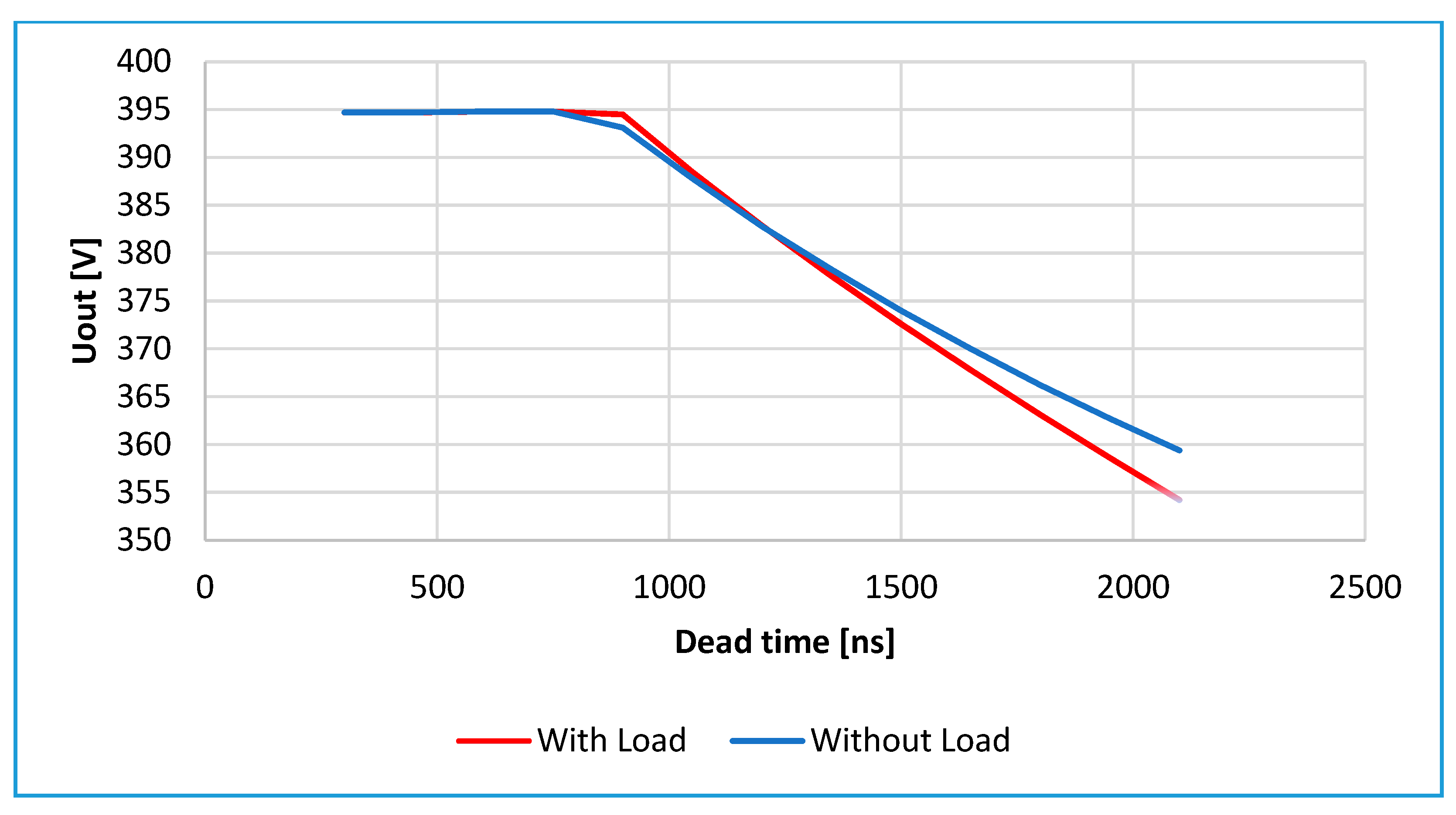
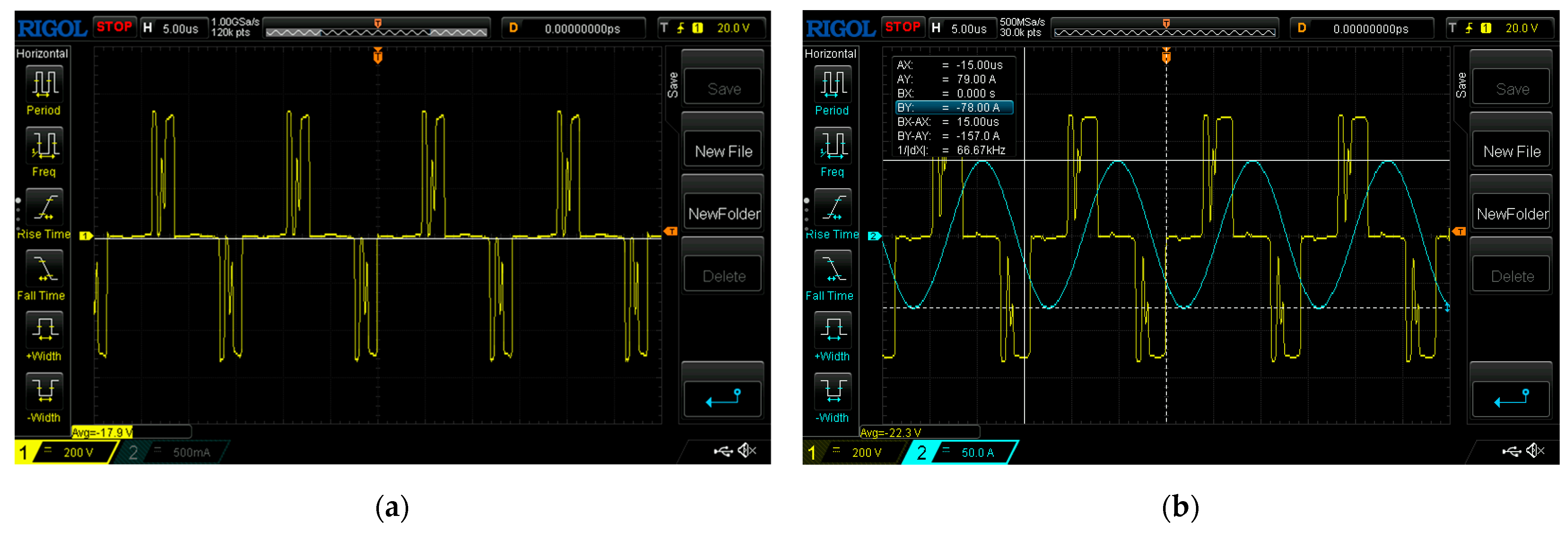
  • Efficiency—a dead-time of 1500 ns did not affect the overall transmission efficiency.
  • Power quality—the influence of the dead-time did not affect the quality of the output voltage waveform on the inverter or the stability of the WPT transmission.
  • Electromagnetic interference (EMI)—the emission of electromagnetic disturbances as a result of the dead-time is aligned with the electromagnetic stability standards. In the proposed system, in the area outside the coils, the magnetic induction values according to the simulation results were lower than the values recommended by the ICNIRP guidelines.
  • Switch stress—the selection of the dead-time considered the maximum possible operating frequency of the IGBTs.
Finally, it can be concluded that the analysis carried out in MATLAB is in agreement with the experimental results. Furthermore, considering its practical use, this WPT implementation can find applications in the process of charging lithium-ion batteries according to the principle of constant current–constant voltage.

4. Conclusions

The procedure used to minimize dead-time effects is explained in detail in this paper. Also, the dead-time adjustment method is applied and investigated in a practical example of wireless transmission. The regulation of dead-time is performed in order to achieve the highest possible power for the given phase angle. In particular, the minimum dead-time due to the switching-off of the IGBTs must be considered in practice.
The dead-time issue in two-phase inverters is a critical factor affecting the performance of two-phase wireless power transfer systems. The compensation topologies, such as the LCC-S, offer a promising solution to reduce the adverse effects of the dead-time, improving the efficiency, power quality, and overall system performance. The primary contribution of this research to the existing findings lies in the conclusion drawn regarding the consistent output voltage, irrespective of the presence or absence of a load, up to a dead time value of 1200 ns. Within the suggested range of 600–1500 ns, the impact of dead time on the output voltage amplitude is observed to be less than 10%. Since WPT technology is still developing, addressing the challenges associated with the dead-time issue could be crucial for unlocking its full potential in various applications.

5. Future Works

Future works will focus on further optimization of the compensation topologies for two-phase inverters. Additionally, the analysis of advanced control strategies and the integration of emerging semiconductor devices in order to minimize the dead-time and enhance the WPT system performance in two-phase configurations should be investigated.

Author Contributions

Conceptualization, V.R. and V.T.; methodology, Ž.D. and P.O.; software, Ž.D.; validation, Z.K., P.O. and Z.V.; formal analysis, M.Š., D.H. and V.R.; investigation, Ž.D.; resources, V.R.; data curation, I.F., V.T.; writing—original draft preparation, D.H. and V.R.; writing—review and editing, V.T. and M.B.; visualization, B.P.; supervision, P.O.; project administration, Z.V., Z.S., M.K. and Z.K. All authors have read and agreed to the published version of the manuscript.

Funding

This research was funded by projects 2020-1.1.2-PIACI-KFI-2020-00166 and 2020-1.1.2-PIACI-KFI-2020-00173 of the University of Dunaujavaros and by project GINOP_PLUSZ-2.1.1-21-2022-00249 of the University of Obuda, co-financed by the Hungarian State.

Data Availability Statement

Data is contained within the article.

Acknowledgments

The authors would like to thank the editors and the anonymous reviewers for their valuable comments, which significantly improved the quality of this paper.

Conflicts of Interest

The authors declare no conflicts of interest.

References

  1. Tsiropoulou, E.E.; Mitsis, G.; Papavassiliou, S. Interest-aware Energy Collection & Resource Management in Machine to Machine Communications. Ad. Hoc. Netw. 2018, 68, 48–57. [Google Scholar]
  2. Kim, T.-H.; Yun, G.-H.; Lee, W.Y.; Yook, J.-G. Asymmetric Coil Structures for Highly Efficient Wireless Power Transfer Systems. IEEE Trans. Microw. Theory Technol. 2018, 66, 3443–3451. [Google Scholar] [CrossRef]
  3. Kim, T.-H.; Yoon, S.; Yook, J.-G.; Yun, G.-H.; Lee, W.Y. Evaluation of power transfer efficiency with ferrite sheets in WPT system. In Proceedings of the 2017 IEEE Wireless Power Transfer Conference (WPTC), Taipei, Taiwan, 10–12 May 2017. [Google Scholar]
  4. Yang, J.; Zhang, X.; Zhang, K.; Cui, X.; Jiao, C.; Yang, X. Design of LCC-S Compensation Topology and Optimization of Misalignment Tolerance for Inductive Power Transfer. IEEE Access 2020, 8, 191309–191318. [Google Scholar] [CrossRef]
  5. Pahlavan, S.; Shooshtari, M.; Jafarabadi Ashtiani, S. Star-Shaped Coils in the Transmitter Array for Receiver Rotation Tolerance in Free-Moving Wireless Power Transfer Applications. Energies 2022, 15, 8643. [Google Scholar] [CrossRef]
  6. Pahlavan, S.; Jafarabadi Ashtiani, S. Rotation-Tolerant Wireless Power Transmission Scheme with Smart Positioning for Cognitive Research on Moving Animals. IEEE Trans. Biomed. Circuits Syst. 2023, 1–8. [Google Scholar] [CrossRef]
  7. Cheng, C.; Wang, C.; Zhou, Z.; Li, W.; Deng, Z.; Mi, C.C. Repeater coil-based wireless power transfersystem powering multiple gate drivers ofseries-connected IGBTs. IET Power Electron. 2020, 13, 1722–1728. [Google Scholar] [CrossRef]
  8. Li, S.; Li, W.; Deng, J.; Nguyen, T.D.; Mi, C.C. A Double-Sided LCC Compensation Network and Its Tuning Method forWireless Power Transfer. IEEE Trans. Veh. Technol. 2015, 64, 2261–2273. [Google Scholar] [CrossRef]
  9. Diekhans, T.; De Doncker, R.W. A dual-side controlled inductive power transfer system optimized for large coupling factor variations and partial load. IEEE Trans. Power Electron. 2015, 30, 6320–6328. [Google Scholar] [CrossRef]
  10. Zhang, Z.; Wang, F.; Costinett, D.J.; Tolbert, L.M. Dead-time optimization of SiC devices for voltage source converter. In Proceedings of the 2015 IEEE Applied Power Electronics Conference and Exposition (APEC), Charlotte, NC, USA, 15–19 March 2015; pp. 1145–1152. [Google Scholar]
  11. Zhang, X.; Lai, Z.; Xiong, R.; Li, Z.; Zhang, Z.; Song, L. Switching Device Dead Time Optimization of Resonant Double-Sided LCC Wireless Charging System for Electric Vehicles. Energies 2017, 10, 1772. [Google Scholar] [CrossRef]
  12. Attaianese, C.; Nardi, V.; Tomasso, G. A novel SVM strategy for VSI dead-time-effect reduction. IEEE Trans. Ind. Appl. 2015, 41, 1667–1674. [Google Scholar] [CrossRef]
  13. Choi, J.S.; Yoo, J.Y.; Lim, S.W.; Kim, Y.S. A novel dead time minimization algorithm of the PWM inverter. In Proceedings of the 1999 IEEE Industry Applications Conference (Thirty-Forth IAS Annual Meeting), Phoenix, AZ, USA, 3–7 October 1999; Volume 4, pp. 2188–2193. [Google Scholar]
  14. Dyer, J.; Zhang, Z.; Wang, F.; Costinett, D.; Tolbert, L.M.; Blalock, B.J. Dead-time optimization for SiC based voltage source converters using online condition monitoring. In Proceedings of the 2017 IEEE 5th Workshop on Wide Bandgap Power Devices and Applications (WiPDA), Albuquerque, NM, USA, 30 October–1 November 2017; IEEE: New York, NY, USA, 2017; pp. 15–19. [Google Scholar]
  15. Ji, Y.; Yang, Y.; Zhou, J.; Ding, H.; Guo, X.; Padmanaban, S. Control Strategies of Mitigating Dead-time Effect on Power Converters: An Overview. Electronics 2019, 8, 196. [Google Scholar] [CrossRef]
  16. Urasaki, N.; Senjyu, T.; Uezato, K.; Funabashi, T. An adaptive dead-time compensation strategy for voltage source inverter fed motor drives. IEEE Trans. Power Electron. 2005, 20, 1150–1160. [Google Scholar] [CrossRef]
  17. Patel, P.J.; Patel, V.; Tekwani, P.N. Pulse-based dead-time compensation method for self-balancing space vector pulse width-modulated scheme used in a three-level inverter-fed induction motor drive. IET Power Electron. 2011, 4, 624–631. [Google Scholar] [CrossRef]
  18. Martínez, A.; González, C.; Jaramillo, A.; Cárdenas, D.; Von Chong, A. Experimental data validating the optimization of a wireless power transfer prototype employing a novel phase shift measurement system and frequency control. Data Brief 2022, 45, 108675. [Google Scholar] [CrossRef]
  19. Xu, F.; Huang, H. Frequency selection for underwater wireless power transfer based on the analysis of eddy current loss. AEU Int. J. Electron. Commun. 2023, 163, 154618. [Google Scholar] [CrossRef]
  20. Schormans, M.; Valente, V.; Demosthenous, A. Frequency Splitting Analysis and Compensation Method for Inductive Wireless Powering of Implantable Biosensors. Sensors 2016, 16, 1229. [Google Scholar] [CrossRef]
  21. Li, W.; Diao, L.; Mei, W.; Dongye, Z.; Qin, X.; Jin, Z. Optimized Resonant Network Design for High Energy Transfer Efficiency of the WPT System. Electronics 2023, 12, 1984. [Google Scholar] [CrossRef]
  22. Rong, C.; Wu, Z.; Yan, L.; Chen, M.; Yan, J.; Ren, G.; Xia, C. Research on Tuning Control Technology for Wireless Power Transfer Systems for Concrete Embedded Sensors. Electronics 2023, 12, 3963. [Google Scholar] [CrossRef]
  23. Solouma, N.H.; Kassahun, H.B.; Alsharafi, A.S.; Syed, A.; Gardner, M.R.; Alsharafi, S.S. Alsharafi: An Efficient Design of Inductive Transmitter and Receiver Coils for Wireless Power Transmission. Electronics 2023, 12, 564. [Google Scholar] [CrossRef]
  24. Liu, X.; Wang, T.; Jin, N.; Habib, S.; Ali, M.; Yang, X.; Tang, H. Analysis and Elimination of Dead-Time Effect in Wireless Power Transfer System. Energies 2018, 11, 1577. [Google Scholar] [CrossRef]
  25. Zhao, B.; Song, Q.; Liu, W.; Sun, Y. Dead-Time Effect of the High-Frequency Isolated Bidirectional Full-Bridge DC–DC Converter:Comprehensive Theoretical Analysis and Experimental Verification. IEEE Trans. Power Electron. 2014, 29, 1667–1680. [Google Scholar] [CrossRef]
  26. Chen, Y.; Zhang, H.; Park, S.-J.; Kim, D.-H. A Switching Hybrid LCC-S Compensation Topology for Constant Current/Voltage EV Wireless Charging. IEEE Access 2019, 7, 133924–133935. [Google Scholar] [CrossRef]
  27. Kadavelugu, A.; Baek, S.; Dutta, S.; Bhattacharya, S.; Das, M.; Agarwal, A.; Scofield, J. High-frequency Design Considerations of Dual Active Bridge 1200 V SiC MOSFET DC-DC Converter. In Proceedings of the 2011 Twenty-Sixth Annual IEEE Applied Power Electronics Conference and Exposition (APEC), Fort Worth, TX, USA, 6–11 March 2011. [Google Scholar]
  28. Vaka, R.; Keshri, R.K. Reconfigurable WPT system for loadindependent CC and CV output with transmitting-side control. IET Electr. Power Appl. 2020, 14, 685–694. [Google Scholar] [CrossRef]
  29. Wang, D.; Peng, F.; Ye, J.; Yang, Y.; Emadi, A. Dead-time effect analysis of a three-phase dual-active bridge DC/DC converter. IET Power Electron. 2018, 11, 984–994. [Google Scholar] [CrossRef]
  30. Zammit, D.; Staines, C.P.; Apap, M. Dead Time Compensation in H-Bridge Inverters. Int. J. Ind. Electron. Drives 2018, 4, 1. [Google Scholar] [CrossRef]
  31. Bai, H.; Mi, C.C.; Gargies, S. The Short-Time-Scale Transient Processes in High-Voltage and High-Power Isolated Bidirectional DC–DC Converters. IEEE Trans. Power Electron. 2008, 23, 2648–2656. [Google Scholar] [CrossRef]
  32. Song, C.; Chen, A.; Chen, J.; Du, C.; Zhang, C. Dead-Time Effect Analysis of Dual Active Bridge DC-DC Converter with Dual-Phase-Shift Control. In Proceedings of the IEEE Chinese Automation Congress (CAC), Jinan, China, 20–22 October 2017. [Google Scholar] [CrossRef]
  33. Three-Phase Diode Sleeper. Available online: https://datasheetspdf.com/pdf/1391461/GoldElectric/MDQ150A1600V/1 (accessed on 2 November 2023).
  34. Evaluation Board EVAL-1ED3491Mx12M. Available online: https://www.infineon.com/cms/en/product/evaluation-boards/eval-1ed3491mx12m/ (accessed on 2 November 2023).
  35. Toshiba MG50Q2YS50. Available online: https://datasheetspdf.com/pdf-file/425956/Toshiba/MG50Q2YS50/1 (accessed on 2 November 2023).
Figure 1. Switching characteristics and the equivalent circuit operation of two-phase inverters without IGBT dead-time. (a) Characteristic signals for a two-phase inverter without IGBT dead-time. (b) Equivalent circuit operation of two-phase inverters.
Electronics 13 00304 g001
Figure 2. Switching characteristics and equivalent circuit operation of two-phase inverters with IGBTs dead-time. (a) Characteristic signals for a two-phase inverter with IGBTs dead-time. (b) Equivalent circuit operation of two-phase inverters.
Electronics 13 00304 g002
Figure 3. The circuit of the WPT system with an LCC-S resonant compensation network.
Electronics 13 00304 g003
Figure 4. The equivalent electrical circuit of the WPT system with an LCC-S resonant compensation network with a load.
Electronics 13 00304 g004
Figure 5. Model of the WPT system with an LCC-S resonant compensation network in MATLAB.
Electronics 13 00304 g005
Figure 6. (a) Inverter output voltage waveform; (b) inverter output current waveform.
Electronics 13 00304 g006
Figure 7. Effect of the dead-time on the output voltage.
Electronics 13 00304 g007
Figure 8. Experiment platform. (a) Prototype of the WPT system; (b) elements of the inverter with a special driver and a half-bridge made with IGBTs.
Electronics 13 00304 g008
Figure 9. Voltage and current of the inverter circuit. (a) The waveform of the voltage of the transmitting coil. (b) The waveform of the current and voltage of the transmitting coil.
Electronics 13 00304 g009
Table 1. LCC-S resonant WPT system parameters.
ParameterLabelValue
Primary coilL_GA38.5 uH
Secondary coilL_VA46.4 uH
Mutual inductorM8.13 uH
Primary series capacitorC_GA210 nF
Secondary series capacitorC_VA115 nF
Primary parallel capacitorCf375 nF
Primary series inductorLf13.8 uH
Output equivalent resistanceRload22 Ω
Disclaimer/Publisher’s Note: The statements, opinions and data contained in all publications are solely those of the individual author(s) and contributor(s) and not of MDPI and/or the editor(s). MDPI and/or the editor(s) disclaim responsibility for any injury to people or property resulting from any ideas, methods, instructions or products referred to in the content.

