Article

Mitigation of Low Harmonic Ripples Based on the Three-Phase Dual Active Bridge Converter in Charging Station Applications

1
Department of Electrical Engineering, Aichi Institute of Technology, Yachigusa-1247 Yakusacho, Toyota 470-0356, Aichi, Japan
2
School of Electrical and Electronics Engineering, Hanoi University of Science and Technology, Hanoi 100000, Vietnam
3
EVSELab, Co., Ltd., Hanoi 100000, Vietnam
*
Author to whom correspondence should be addressed.
Electronics 2024, 13(13), 2527; https://doi.org/10.3390/electronics13132527
Submission received: 8 May 2024 / Revised: 19 June 2024 / Accepted: 24 June 2024 / Published: 27 June 2024

Abstract

:
To minimize the recharge time of EVs, Level 3 charging stations utilizing DC fast charging systems have become increasingly prevalent. Additionally, these systems offer bidirectional functionality, aiding in stabilizing the DC grid during peak hour. As a result, the DC–DC converters utilized in such systems must be capable of bidirectional energy transfer. Among existing typologies, DAB converters are preferred due to their simplicity and sustainability. The three-phase DAB (DAB3) is favored because the output ripple is lower compared to the single-phase structure. This characteristic assists in mitigating the negative effects on the battery caused by high-frequency current ripple. However, the input to DAB3 converters typically originates from AC–DC stages, leading to the inclusion of low harmonic frequency ripples (e.g., multiples of 360 Hz). These ripples are then transferred to the battery, increasing its temperature. To address this issue, this paper proposes a technique to mitigate negative effects by attenuating these low frequencies in the charging current. Simulations were conducted to demonstrate the effectiveness of the proposed technique. Scaled-down experiments utilizing a DAB3 prototype were conducted to corroborate the simulations. The findings demonstrated a reduction in ripple from 8.66% to below 2.67% when compared to the original controller. This reduction enabled the solution to meet the limiting current ripple criteria outlined in the CHAdeMO standard.

1. Introduction

According to the Global EVs Outlook 2023 [1], the number of electric vehicles (EVs) grew more than tenfold in the span of five years leading up to 2022. Furthermore, this growth trend is anticipated to continue exponentially in the coming years, aiming to achieve net zero emissions by 2050 [2]. For example, battery electric vehicles (BEVs) have seen significant market share expansion since 2014. The batteries and corresponding charging systems employed in these BEVs are crucial factors influencing their efficiency and pricing. Consequently, various companies are intensifying their research efforts into BEV charging technologies, to sustain their growth rates in the foreseeable future [3,4,5].
Among several factors such as optimized structural design with fewer components, safety measures, high efficiency, fast charging, etc., charging technology stands out as one of the most attractive research topics [6]. These technologies are typically classified into two main categories: wired charging technologies (or contact charging) [7] and wireless charging technologies (or contactless charging) [8,9]. However, this paper focuses solely on wired charging. Wired charging technologies necessitate a direct connection between the EV and the charging system, via cables for charging purposes. These technologies can be further subdivided into AC charging technologies and DC charging technologies. While AC charging technology was discussed in [7,10], this paper concentrates on the charging station, thus delving into the details of DC charging.
DC charging technologies enable direct charging to the battery [11], thereby offering fast charging capabilities. Additionally, these technologies contribute to an overall reduction in the size and weight of the driving system, since the charging unit is separate from the vehicle. However, they are not flexible in terms of charging locations, as they are typically operated at high power levels (hundreds of kW); thus, a fixed installation location is mandatory. Nevertheless, they offer another feature known as vehicle-to-grid (V2G) technology. This allows vehicles to transfer energy back to the grid to help stabilize it during peak hours. Recently, V2G technology has attracted significant attention from researchers, as evidenced by publications in [12,13,14,15].
To enable V2G functionality in a charging station, a key requirement is for the DC–DC converter to be bidirectional. Among the various converter typologies [16,17,18], two promising candidates stand out: the dual-active bridge (DAB) type converters [19,20,21] and the CLLC resonance type converters [22,23]. Both types of converters offer critical characteristics, such as bidirectionality, galvanic isolation, soft switching capability, and high power density. However, the DAB type converters are preferred, due to their simple structure and sustainability.
The DAB type can be categorized into two types: single-phase [19] and three-phase [21]. In comparison with the single-phase DAB [24], the three-phase variant achieves lower phase RMS current and output current ripple. This reduction in output current ripple not only leads to a decrease in capacitor size but also enhances the quality of the charging current, thereby contributing to an increase in battery lifetime. Consequently, this paper focuses on the three-phase structure instead of the single-phase topology.
While a three-phase DAB (DAB3) converter can mitigate the negative effects of high-frequency current ripple on the battery, the AC–DC stages are typically put in the front of the DC–DC stage in charging station applications [25]. These stages are responsible for converting AC voltage to DC voltage before feeding it to the DC–DC stage. There are two main technologies employed for this purpose: multi-pulse rectifiers (six, twelve, or more pulses) and active rectifier structures (such as two-level and three-level neutral-point-clamp (NPC) or Vienna-type rectifiers) [26,27]. Although multi-pulse rectifier technology tends to be bulkier compared to active rectifier types, it is widely utilized in high-power applications, due to its simple structure, high robustness, and relatively low harmonic distortion [28]. There have been several publications on multi-pulse rectifiers that comply with power quality standards such as IEEE-519 [29] and IEC 61000-3-2 [30]. Some of these include [31,32,33]. However, this paper focuses on the DC–DC stage, to improve the charging current quality of the battery. Therefore, it is reasonable to assume that the AC–DC stage can be supplied with a stable output voltage and meet all necessary quality requirements.
Both technologies generate low-frequency harmonics at the output DC voltage, which can then affect the battery’s lifetime and exceed standard limits when transferred through the DAB3 converter [34]. When low-frequency ripple increases, it elevates stress currents in power switches and magnetic components within the converter, consequently diminishing the energy conversion efficiency of the system. Moreover, the amplitude of peak-to-peak ripple increases in accordance with load requirements, potentially violating standards such as IEC61851-23 and CHAdeMO [34], among others. For example, according to the CHAdeMO standard, a ripple current of 5 kHz or less must be under 3.0 A. This ripple also diminishes the lifetime of both batteries and fuel cells. Hence, addressing low harmonic ripple becomes imperative. In this study, the primary concern is battery health, and thus solutions are focused on improving the quality of the charging current. Utilizing additional active components such as power decoupling circuits [35,36] is not favored, due to the resultant increase in component count.
Due to the relatively low frequency, a substantial bank of electrolytic capacitors has be added to the DC bus. This requirement results in elevated costs and wasted space, ultimately leading to a significant reduction in the power density of the converter [37]. Furthermore, these capacitors serve as critical components that limit the system’s lifetime. According to [38,39], the lifespan of a high-quality electrolytic capacitor is only 3000 to 5000 h and decreases by half with every temperature increase of 10 °C. Consequently, relying on a large bank of capacitors is not considered a viable solution.
Another solution involves utilizing the DC–DC stage to process the low ripple frequency. The controller of the DC–DC stage is meticulously designed to cancel out the ripple, similarly to the approach described in previous works [37,40]. However, these methods involve transferring power flow from the battery to the grid and aim to eliminate the ripple at the DC bus. Consequently, they cannot be applied when the charger operates in constant current (CC) mode. Additionally, these solutions are designed to mitigate specific frequencies (e.g., double line frequency). Therefore, they cannot be directly applied in cases where there are multiple low frequency harmonic ripples.
This study aimed to address the issue of low-frequency ripple reduction occurring at the output terminal of a DAB3 converter supplied by the twenty-four-pulse diode rectifier of a real charging system in Japan. The schematic overview of the system is depicted in Figure 1. The approach was to improve the control system of the DAB3 converter with some resonators that synchronize and mitigate the effect of the low frequency current components. However, due to constraints imposed by the available laboratory resources, a scaled-down experimental setup was utilized, necessitating the reduction of the twenty-four-pulse rectifier to a six-pulse configuration for algorithmic testing purposes. It is noteworthy that an identical approach remains applicable to the original twenty-four-pulse configuration, particularly in scenarios involving high-power applications.
The rest of this paper is structured as follows: Section 2 describes the system configuration and assumptions. The modeling of the DAB3 converter is presented in detail in Section 3. Section 4 shows the controller design and algorithm for mitigation of the low harmonic frequency current ripple. The experiments are detailed in Section 5. Finally, Section 6 summarizes the conclusions and limitations.

2. System Configuration and Assumptions

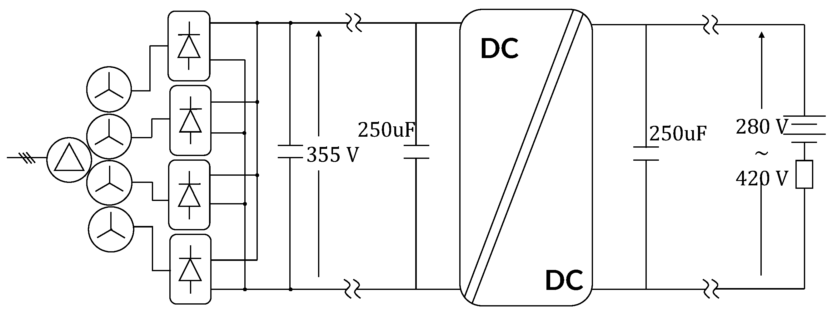
2.1. General Structure

A DC fast charging system typically transforms three-phase AC voltage sourced from the power grid into the direct current (DC) voltage necessary for the charging of electric vehicle (EV) batteries. Illustrated in Figure 1 is a simplified depiction of a fast charging station system. Despite the bulkiness associated with multi-pulse rectifier technology in comparison to active rectifier types, it finds extensive application in high-power scenarios owing to its straightforward configuration, elevated resilience, and comparatively reduced harmonic distortion levels.
As mentioned above, a six-pulse diode rectifier is employed to supply the DC–DC (DAB3) converter. Conventionally, the rectifier’s output exhibits periodicity at a frequency six times that of the line frequency ( f l i n e ), for instance, 360 Hz. Additionally, numerous harmonics are superimposed onto the base frequency of 360 Hz. A comprehensive analysis of the harmonic amplitudes is provided.
Let us first consider a three-pulse rectifier as illustrated in Figure 2. In a three-pulse input rectifier, there are three sources, V A , V B , and V C , with the same amplitude, frequency, and offset at an angle of 120 degrees, connected to each other. Additionally, the diodes D 1 , D 2 , and D 3 are of the common cathode configuration. The output load ( R L o a d ) is connected between the common cathode terminal and ground. The output voltage exhibits periodicity at the frequency of 3 f l i n e , and it can be described in Fourier form as shown by Equation (1).
v o , t h r e e p u l s e ( t ) = V a v g + n = 1 a n cos 2 π n t T + b n sin ( 2 π n t T )
Let T = 1 / f l i n e , ω 0 = 2 π f l i n e , V p k denote the peak value of each phase input, and let V a v g represent the average output rectifier voltage, which can be determined by Equation (2). The parameters b n and a n are defined as shown in Equations (3) and (4), respectively.
V a v g = 3 3 V p k 2 π
b n = 2 2 π / 3 π 3 π 3 V p k sin ( ω 0 t ) sin ( n ω t ) d ( ω t )
a n = 2 2 π / 3 π 3 π 3 V p k sin ( ω 0 t ) cos ( n ω t ) d ( ω t )
It is evident that b n equals zero, as it represents an even function within this interval. The simplified equation for a n can be derived using Equation (5).
a n = 3 3 V p k π ( 1 n 2 ) cos n π 3
The Fourier series of the three-pulse rectifier can be derived according to Equation (6).
v o , t h r e e p u l s e ( t ) = 3 3 V p k 2 π + n = 1 3 3 V p k π ( 1 n 2 ) cos n π 3 cos 2 π n t T
with n = 3 , 6 , 9 ,
Utilizing the outcomes from the analysis of the three-pulse rectifier, as shown in Equation (6), the Fourier analysis of the six-pulse case (illustrated in Figure 3) can be readily determined by subtracting the voltages at the positive ( v p ) and negative ( v n ) phases. The expressions for v p and v n are described by Equations (7) and (8), respectively.
v p = 3 3 V p k 2 π + 3 3 V p k 8 π cos ( 3 ω 0 t ) 3 3 V p k 35 π cos ( 6 ω 0 t ) + 3 3 V p k 80 π cos ( 9 ω 0 t ) +
v n = 3 3 V p k 2 π 3 3 V p k 8 π cos ( 3 ω 0 t ) 3 3 V p k 35 π cos ( 6 ω 0 t ) 3 3 V p k 80 π cos ( 9 ω 0 t ) +
Then, the output voltage of the six-pulse rectifier can be determined by Equation (9)
v o , s i x p u l s e = v p v n = 3 3 V p k π 6 3 V p k 35 π cos ( 6 ω 0 t ) 6 3 V p k 143 π cos ( 12 ω 0 t )
According to Equation (9), the output ripple exhibits numerous frequency harmonics with a fundamental frequency of 6 f l i n e . Notably, the amplitude of the fundamental harmonic is only four times greater than that of the second harmonic, and about nine times higher than that of the third. The amplitude is even smaller at higher frequency harmonics, as shown by Figure 4 (with 1 p.u. = V p k ). Consequently, the charging current may contain these frequency ripples, which can potentially yield adverse effects on the battery and may also lead to non-compliance with standards such as CHAdeMO.
This paper delineates a control technique aimed at mitigating the adverse effects on the battery caused by the aforementioned low-frequency ripples. The control strategy is implemented using a DAB3 converter.

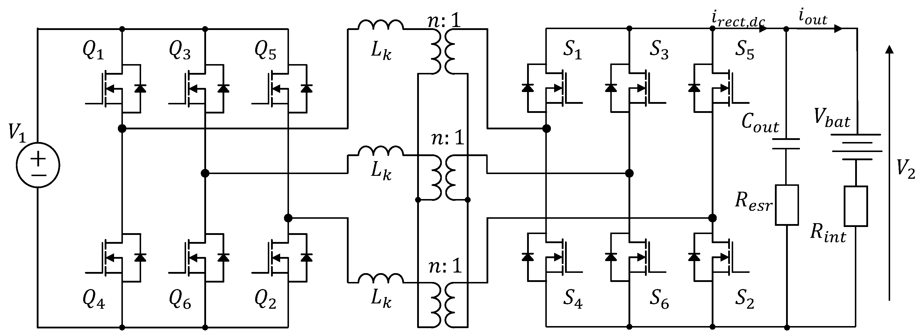
2.2. The Three-Phase Dual Active Bridge Converter

Figure 5 depicts the topology of the DAB3 converter. The transformers are constituted by three single-phase transformers connected in a star–star configuration. Each transformer possesses a leakage inductance denoted by L k and a winding ratio of n : 1 . At both ends of the transformer, there are two three-phase inverters. The MOSFETs belonging to the primary and secondary inverters are designated with the letters Q and S, respectively. The input voltage ( V 1 ) is provided by the previous rectifier stage. The output voltage ( V 2 ) is the battery voltage. The output capacitor ( C o u t ) serves as a voltage stabilization filter. In addition, this paper also considers the component equivalent series resistance ( R e s r ) of the capacitor and the resistance of the parasitic component ( R i n t ).
In this analysis, the conventional single-phase-shift (SPS) modulation scheme is employed. The modulation scheme and several key current waveforms are illustrated in Figure 6. In this modulation technique, each MOSFET conducts for 180 degrees within one period. Simultaneously, they are complementary modulated within the same leg, and a dead-time is inserted between the gate signals to prevent shoot-through phenomena. Within each inverter, two legs exhibit a phase shift of 120 degrees. The power flow is regulated by adjusting the phase shift ( φ ) between the primary and secondary sides.
In order to simplify the analysis, some assumptions are made as follows:
  • Series resistance of the transformer winding is ignored;
  • ON resistance of the MOSFETs is ignored;
  • Parameters of switches are identical;
  • Parameters of transformers are identical;
  • Magnetizing inductance is much higher than the leakage inductance;
  • The voltage drops across the parasitic resistors are significantly smaller than the voltage of the battery;
  • The AC–DC stage can be supplied with a stable output and satisfy requirements at the AC line input.
The output voltages of phase x primary ( v p x ) and secondary ( v s x ), indexed as a, b, or c, exhibit a waveform characterized by six steps and are phase-shifted by an angle φ . By considering the overlap between v p x and v s x , twelve intervals are delineated. The phase current, represented by the red, black, and blue curves in Figure 6, can be determined accordingly. The transition currents of Phase A (including MOSFETs Q 1 and Q 4 ) can be calculated using Equation (10).
I a 0 = I M 2 ( 1 M ) + 3 M φ π I a 1 = I M 2 ( 1 M ) + 3 φ π I a 2 = I M ( 1 M ) + 3 M φ π I a 3 = I M ( 1 M ) + 6 φ π I a 4 = I M ( 1 M ) + 6 M φ π I a 5 = I M ( 1 M ) + 3 φ π
where I M = V 1 6 X d , X d = 3 f s L k with f s being the switching frequency; M = n V 2 V 1 is the equivalence turn ratio between the secondary and primary side referred to the primary side.
Based on these transition current values, let φ be within the range of [ π 3 , π 3 ] to avoid high RMS current. The power transfer ( P o u t ) can be determined using Equation (11).
P o u t = 3 M V 1 I M 2 π φ 4 3 φ π

3. Modeling

State-space averaging is a prevalent technique utilized for modeling the stability of switched converters, and it has been effectively employed in the analysis of single-phase dual active converters. As delineated in Section 2, the voltage across the terminals of the inductor remains constant within six intervals over half a period. These discrete states are instrumental in facilitating the application of the state-space averaging methodology.
From the DAB3 topology as shown in Figure 5, there are total four storage elements ( L k 1 , L k 2 , L k 3 , and C o u t ). This means the system is fourth-order. However, the DAB-type converters belong to the class of a variable structure system. Specifically, phase currents are fast changing compared with the output voltage. Luckily, the working frequency operation of the control system is much lower than the switching frequency. Therefore, the fast changing variable can be ignored. The order of the system is then reduced to one. The average state space presented for the system is shown by Equation (12)
x ˙ = A x + B u y = C x + D u
where x and y are both presented for v 2 ; u is a matrix of [ v 1 , v b a t ] T with v b a t is the battery voltage; C = 1; and D = 0.
To derive the matrices A 1 × 1 and B 1 × 2 , the node equation governing the output capacitor is employed, as depicted in Equation (13).
d v 2 d t = 1 C o u t ( i r e c t , d c i o u t )
where i r e c t , d c is the output rectification, and i o u t is the output charging current to the battery.
The large signal equation is derived from this equation and is expressed by Equation (14), where the overbar notation denotes the average value of the parameters.
d v 2 ¯ d t = 1 C o u t ( i r e c t , d c ¯ i o u t ¯ )
To obtain this large signal model, it is necessary to determine the value of i r e c t , d c . The frequency of the output ripple is six times that of the switching frequency. Consequently, only the average currents during intervals I and I I need to be determined. Referring to Figure 6, the upper state of the MOSFET at the secondary side is identified. Subsequently, the average current in each interval can be calculated using Equation (15).
i r e c t , d c , M ¯ = x = 1 3 S s x , M × i L x , M ¯
Let S s x , M represent the switching function of the output side of phase x (presented by subscripts a , b , and c), during interval M ( I , I I , etc). Specifically, S s x , M equals zero when the top side is in the OFF state, and it equals one otherwise. These values can be calculated using Equations (16) and (17), which correspond to the phase shift in the range of [ φ , π 3 ] and [ π 3 , π 3 + φ ] , respectively.
i r e c t , d c , I ¯ = i L c , I ¯
i r e c t , d c , I I ¯ = i L a , I I ¯ + i L c , I I ¯
Following Equation (10), Equations (16) and (17) can be simplified as follows:
i r e c t , d c , I I ¯ = I M 1 M + 3 φ 2 π ( 2 M + 1 )
i r e c t , d c , I I ¯ = 3 I M ( 1 + M )
Utilizing the symmetry of the i r e c t , d c current, the average output current for the odd intervals is identical, as is the case for the even intervals. Here, “odd” indexing denotes the odd interval [ φ , π 3 ] , while “even” indexing denotes the alternative case. By substituting Equations (16), (17) and (12) into Equation (14), Matrices A o d d ; A e v e n and B o d d ; B e v e n can be determined using the following equations:
A o d d = R i n t ( 3 φ π ) 9 ω s L k 9 ω s L k C o u t ( R e s r + R i n t ) B o d d = R i n t 9 ω s L k C o u t ( R e s r + R i n t ) 1 3 φ + π , 1 C o u t
A e v e n = 3 ( φ R i n t 3 ω s L k ) 9 ω s L k C o u t ( R e s r + R i n t ) B e v e n = 3 ( φ R i n t 3 ω s L k ) 9 ω s L k C o u t ( R e s r + R i n t ) , 1 C o u t
Let ω s = 2 π f s , then from Equations (20) and (21), the average matrices A and B can be determined as follows:
A = 1 π / 3 × π 3 φ A e v e n + φ A o d d = 1 ( R b a t + R e s r ) C o u t B = 1 π / 3 × π 3 φ B e v e n + φ B o d d = R i n t φ ( R e s r + R i n t ) ω s L k C o u t 2 3 φ 2 π , 1 C o u t
From here, the equilibrium point can be obtained by solving the following equation:
A v 2 ¯ + B [ V 1 V b a t ] T = 0
By linearizing around the equilibrium point, the small signal model can be obtained as depicted in Equation (24).
v 2 ( s ) φ ( s ) = ( R e s r C o u t + 1 ) V 1 R i n t [ ( R e s r + R i n t ) C o u t s + 1 ] ω s L k 2 3 φ π
Under the assumption that the voltage drop across the battery resistor is significantly smaller than the output voltage, the transfer function from control input to output current can be derived using Equation (25).
i o u t ( s ) φ ( s ) = ( R e s r C o u t + 1 ) V 1 ( R e s r + R i n t ) C o u t s + 1 ω s L k 2 3 φ π
In this paper, significant emphasis is placed on the constant current (CC) charging mode. The transfer function from control input to output current, as illustrated in Equation (25), reveals that this relationship is independent of the load. Consequently, the DAB3 converter can be regarded as a current source, offering advantages in terms of ease of control.

4. Controller Design and the Low Harmonic Frequency Current Ripple Mitigation Algorithm

In the operation of the DAB3 converter, control is executed through the utilization of a proportional and integral (PI) controller to effectively regulate both the DC voltage and current, to achieve error-free conditions during steady-state operation. This is primarily attributed to the infinite gain characteristic of the PI controller at direct current (DC) frequencies (0 Hz).
Consequently, in order to address the presence of low harmonic frequency ripple phenomena (e.g., at 360, 720, and 1080 Hz), the PI controller requires a design configuration featuring a high bandwidth within the current loop. This design approach ensures that the gain at these frequencies is sufficiently high, thereby mitigating the amplitude of ripple occurrences. Nonetheless, the bandwidth of the current loop is inherently constrained by the frequency limitations of the low-pass filter and the dynamic demands inherent to battery charging applications. For instance, in the context of battery charging processes, stringent requirements dictate that the current slew rate does not surpass 20 A/s, with shutdown slew rates falling within the range of 100–200 A/s [34]. Consequently, opting to increase the bandwidth to accommodate low-frequency current ripple may not constitute an optimal course of action.

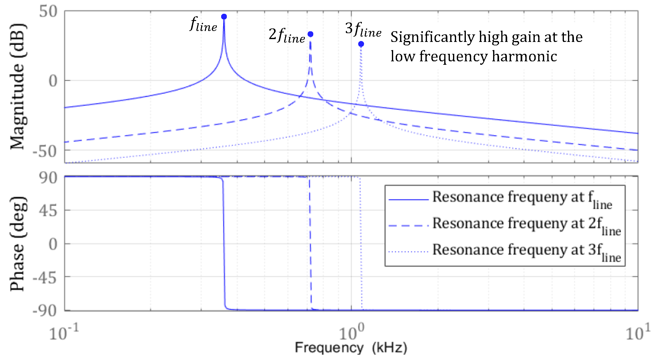
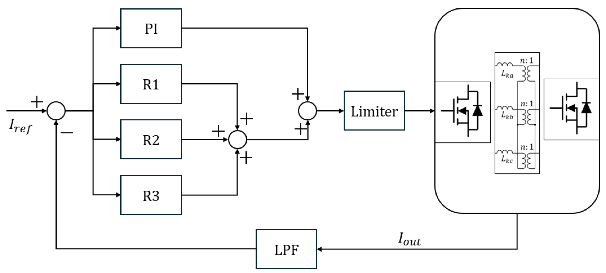
4.1. Multiple Resonance Controllers

As a well-known resonance (R) controller employed for the precise regulation of signals at a specific frequency, it is essential to consider its ideal characteristics. Ideally, the transfer function governing the R term can be represented by Equation (26). Notably, this transfer function exhibits infinite gain precisely at the frequency denoted by ω rad/s. Consequently, signals possessing this specific frequency can be effectively managed utilizing the capabilities of the R controller.
G R ( s ) = 2 k i r s s 2 + ω 0 2
where k i r are the design parameters, and ω 0 is the resonance frequency.
The bode plot depicted in Figure 7 illustrates the characteristic response of an ideal R controller, represented by the blue curve. As previously noted, the gain exhibited at the resonance frequency is notably elevated, effectively facilitating the suppression of low-frequency ripple phenomena. However, it is imperative to acknowledge the inherent sensitivity of the controller, stemming from its heightened gain solely at the precise resonance frequency. Consequently, even minor deviations from this frequency can result in the persistence of low-frequency components. For instance, in the scenario presented herein, wherein the frequency ripple transitions from 360 Hz to 356.4 Hz (about 1% line frequency reduction), the gain of the ideal R controller experiences a shift from 122 dB to 12.2 dB. This diminished gain becomes further pronounced with an escalation in the disparity between the low-frequency ripple and the resonance frequency.
To avoid this sensitivity, a modified resonance controller can be applied. Its transfer function is expressed in Equation (27). Additional parameters ω 0 are used to make the R controller less sensitive than the ideal model. Three cases of ω 0 are considered to realize its effect to the controller. As the results show, the peak of R controller at the resonance frequency is reduced compared with the previous time, but it still remains high enough to deal with the low frequency ripple (about 50 dB). Moreover, it can achieve a relatively high gain at the frequencies around the resonance point. However, ω 0 should not be greatly increased, because the gain is also increased. Hence, the system stability can be effected as the phase margin of the system is decreased.
G R ( s ) = 2 k i r ω c s s 2 + 2 ω c s + ω 0 2
In scenarios involving multiple harmonic frequency ripples, a similar approach can be adopted by employing multiple R controllers, each configured to address specific harmonic frequencies. As illustrated in Figure 8, distinct resonance peaks correspond to low harmonic frequency ripples, including those at 360 Hz, 720 Hz, and 1080 Hz, which stand for the dominant effect harmonics, as depicted in Figure 4. The structural intricacies and design specifications of these controllers are elaborated upon in the subsequent discourse.

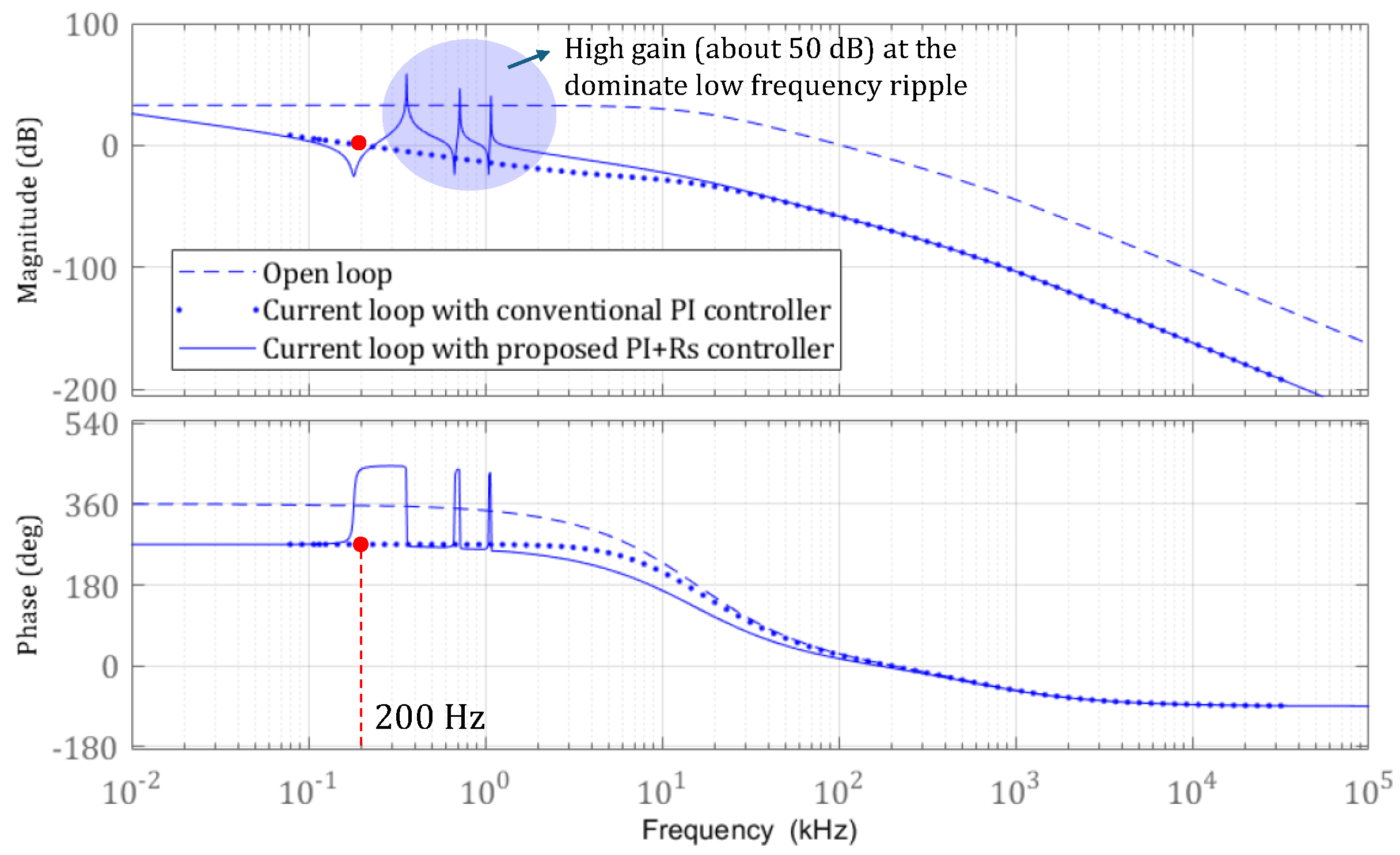
4.2. Controller Design with Harmonic Frequency Ripple Cancellation

In accordance with the CHAdeMO standard, the constraints on current ripple are delineated in Table 1. Specifically, for ripples occurring at frequencies below 5 kHz, the peak-to-peak amplitude must not exceed 3 A. As demonstrated in Equation (9), the bus voltage of the DAB3 converter experiences perturbations from multiple harmonics, with a fundamental frequency of 360 Hz. Among these harmonics, the amplitudes of the first three are particularly influential, as shown in Figure 4, and thus necessitate careful consideration during controller design.
The current control loop employs a conventional PI controller to regulate the DC component, while three modified R controllers are utilized to address the harmonic frequency ripples, as previously discussed. This arrangement is illustrated in Figure 9. As the frequency of the disturbance harmonics increases, additional modified R controllers are incorporated. Furthermore, the voltage control loop can remain configured as an outer loop to the current control loop, operating in constant voltage (CV) mode. However, the primary focus lies in minimizing low-frequency ripple, thus only parameters pertaining to the current control loop are designed. Subsequently, the efficacy of the resonance term can be validated.
Key parameters of the DAB3 converter essential for controller design and validation are meticulously detailed in Table 2. The converter comprises three single-phase transformers, each integrating a leakage inductance of 12.5 μ H, all sharing a common turn ratio of 1:1. These transformers are interconnected via a Δ / Δ configuration. The input voltage is maintained at 100 VDC, sourced from the output of a three-phase rectifier. The output voltage is fixed at 100 V, accompanied by an output current ( i o u t ) of 15 A. Additionally, the system operates at a frequency of 50 kHz, with a sampling frequency set at 20 μ s per sample.
The design procedure can be divided into two distinct steps: Step 1 involves designing the PI controller, while Step 2 entails incorporating multiple modified R controllers. As previously stated, the load comprises a battery with a slow dynamic response. Consequently, the current loop is designed to operate at frequencies in the range of a few hundred Hertz. In this scenario, the cutoff frequency is designated as 200 Hz, and the phase margin is set at 90 degrees. Figure 10, marked by the blue dotted line, illustrates the obtained results aligning with the anticipated parameters. The PI controller parameters are enumerated in Equation (28):
k p = 0.0024 k i = 32.42
Upon completing the initial step, the resonance terms are introduced in Step 2, as discussed in Figure 7 and Figure 8. While the modified resonance term aids in reducing low harmonic ripples, it concurrently elevates the system gain, leading to a reduction in phase margin. In this context, three R controllers are implemented with resonance frequencies ( ω 0 , ω 1 , and ω 2 ) set at 360 Hz, 720 Hz, and 1080 Hz, respectively. To maintain consistency and ensure adequate gain at resonance frequencies, ω c is fixed at 2 rad/s for all R controllers. Consequently, the only design variables are k i r , x , where x = 1, 2, or 3 denotes the index of the corresponding harmonic ripple. Initially, k i r , 1 is chosen to achieve a sufficiently high gain at the 360 Hz fundamental frequency. Subsequently, k i r , 2 and k i r , 3 are scaled proportionally based on the related amplitude, as outlined in Equation (9). The parameters are explicitly listed in Equation (29). The resulting Bode plot is depicted in Figure 10, which is marked by the blue solid line.
k i r , 0 = 20.0 k i r , 1 = 5.0 k i r , 2 = 2.5
Following [37], the use of a Bode plot may not be suitable when incorporating the R term. To ascertain the stability of the system after adding the R term, a Nyquist diagram of the current loop following the design of the PI+R controllers is drawn and depicted in Figure 11. This plot demonstrates that the diagram does not encircle the point 1 + 0 j in the clockwise direction, and there are no right-half-plane poles present. Consequently, it can be deduced that the system is stable.
The verification of the design parameters was conducted through simulations, with the results presented in Figure 12. Two cases were simulated: Case 1 involved low power (100 V/15 A), while Case 2 encompassed high power (355 V/50 A). The simulation outcomes for Case 1 are illustrated in Figure 12a,b, while those for Case 2 are depicted in a similar manner. Given that power scaled proportionally with both voltage and current in the two cases, the control parameters remained unchanged. Additionally, to expedite the simulations and reduce data collection, the slew rate of the charging current was set to 200 A/s for the 100 V scenario and 600 A/s for the 355 V scenario. These values ensured compliance with CHAdeMO requirements, while maintaining simulation efficiency. It is worth noting that these slew rates provide a safety margin, ensuring reliability in real-world applications.
In the simulation of the low-power case, without the ripple cancellation technique, the bus voltage exhibited a ripple containing a 360 Hz component with approximately 9.3 V peak-to-peak amplitude (9.3% of the DC bus voltage). This voltage fluctuation induced an intuitive current ripple of 1.67 A (approximately 11.11% of the output current) at the load, with a frequency and phase slightly shifted from the input. The reason for this phenomenon can be discerned from the Bode plot depicted in Figure 10 (blue dotted line), where the magnitudes of frequencies above 360 Hz remain negative, allowing these related frequency ripples to pass through. However, upon applying multiple R controllers, the amplitudes at these harmonics peaked at high gain. For instance, according to Figure 10 (blue solid line), the amplitudes at 360 Hz, 720 Hz, and 1080 Hz remained around 50 dB. Consequently, these current ripples were effectively eliminated, as demonstrated in Figure 12b, with only residual ripples remaining below 0.4 A peak-to-peak (2.67% of the output current) and a voltage ripple of about 11 V peak-to-peak.
The same trend was observed in the case of the 355 V/50 A condition, as depicted in Figure 12a,d. Without the application of the ripple cancellation technique, the input voltage ripple measured approximately 31 V peak-to-peak (about 8.73% of the DC bus voltage). The output ripple amounted to about 4.20 A peak-to-peak, which clearly violates the CHAdeMO standard. However, upon integrating the ripple cancellation technique, the ripple current was reduced to below 1.92 A under a 35 V input ripple (about 9.8% the DC bus), thereby satisfying the standard requirements. This unequivocally demonstrates the effectiveness of the proposed algorithm as described earlier. Subsequent experiments further validated these simulations.
As shown in both simulation scenarios above, the peak of the phase current varied around the peak value of the conventional setup. Based on the loss analysis detailed in [41], it was expected that the converter efficiency would change slightly compared to the conventional case. However, since this is outside the scope of this paper, a detailed analysis is not provided. Moreover, in terms of battery performance, the temperature increase could be significantly improved, meeting standards such CHAdeMO.

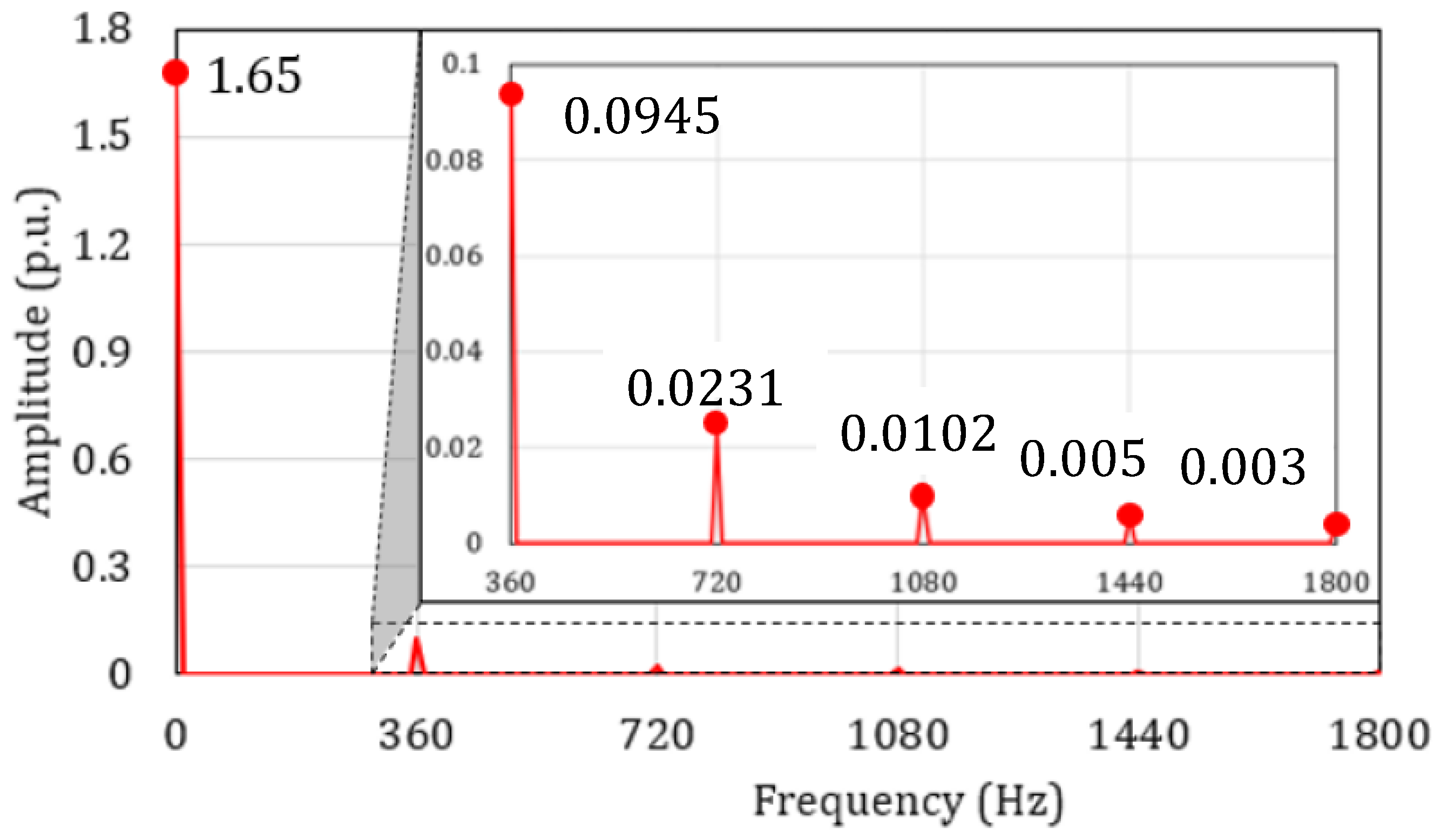
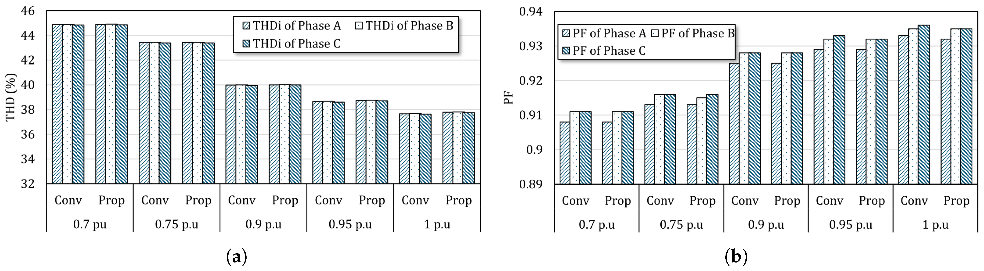
4.3. Analyzing the Effect of THD and PF

In order to analyze the effect of the proposed method on some key parameters of the other stage, PF and THD values were extracted under different load power levels: 0.7 p.u, 0.75 p.u, 0.9 p.u, 0.95 p.u, and 1 p.u (with 1 p.u presented for maximum power), corresponding to the power levels during the CC charging mode. Both conventional and the proposed techniques were considered. A six-pulse rectifier was used for the AC–DC stage during the analysis. The results are summarized and depicted in Figure 13. Specifically, Figure 13a,b show bar plots of THD and PF, respectively, under different power levels. Each group of bars represents the THD or PF for phases A, B, and C. Moreover, the bars are consistently clustered in pairs labeled as “Conv” (conventional) and “Prop” (proposed) for each power level.
For instance, at 0.7 p.u, under the conventional method, the THD of phase currents was around 44–45%, and the PF was around 0.908–0.911 for all phases. These values were almost equal to the proposed method. As power increased, the THD of the phase currents was reduced, but the PF was increased. However, there were still slight differences between the conventional and proposed methods. Therefore, it is summarized that our proposed control method did not significantly affect the THD and PF of the AC line input current.

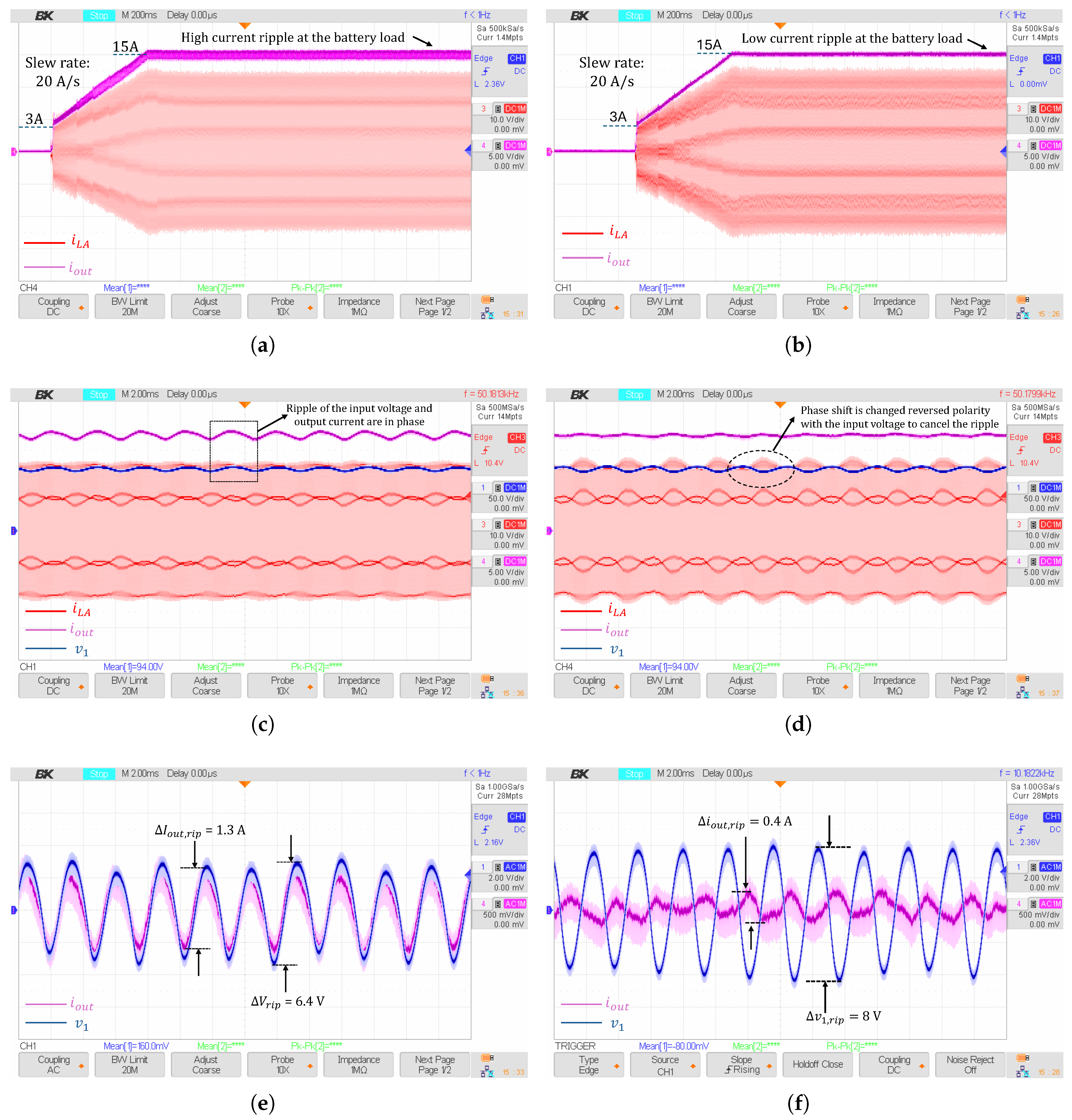
5. Experiment Results

A research experiment was conducted utilizing a DAB3 prototype system, illustrated in Figure 14, to assess the proposed technique. The experimental setup’s crucial parameters are detailed in Table 3. The three-phase rectifier’s output, sourced from a grid simulator (Chroma 61815), was directed to the input of the DAB3 converter. Consequently, harmonics six times the fundamental frequency ( f l i n e ) were generated. The resulting output was connected to an electronic load (Chroma 62120D) configured for constant-voltage operation. Due to experimental constraints, tests were conducted with scaled-down parameters: V 1 = 100 V and V 2 = 100 V. Silicon carbide (SiC) MOSFETs (C2M00025120D from CREE) were employed in both inverters. A three-phase transformer was constructed using three single-phase transformers, yielding an approximate equivalent leakage inductance of 4.25 μ H. Control of the entire system and generation of the switching pattern were facilitated by an STMicroelectronics NUCLEO-STM32G474RE board. Additionally, the output current was monitored using a CP62 current probe from BK Precision, while the phase current was measured with a CWT PEM Rogowski Current Waveform Transducer CWTMini HF3B.
Figure 15 delineates the empirical data pertaining to Case 1 (100 V/15 A), as elucidated in Section 4. Figure 15a,c,e depict the experimental outcomes in the absence of employing the ripple cancellation technique. In contrast, the subsequent cases elucidate the results following the implementation of ripple cancellation. Specifically, the output current exhibited a ramp-up profile with a slew rate of 20 A/s, conforming to the CHAdeMO standard. These experimental findings exhibit a remarkable resemblance to the simulations expounded in Section 4 (Figure 12a,b).
Specifically, in the scenario where the ripple cancellation technique was not applied, at an average bus voltage of 100 V (as depicted in Figure 15d, the observed ripple in measurements was approximately 6.4 V (6.4% of the DC bus), as illustrated in Figure 15e. This ripple resulted in an output current ripple of approximately 1.3 A, constituting approximately 8.66% of the output current. Owing to the design of the low-bandwidth current controller, this ripple aligned closely in phase with the input voltage ripple. Furthermore, this observed value closely matched the simulated ripple of 1.6 A (as depicted in Figure 12a).
Figure 15b,d present the outcomes when employing the ripple cancellation technique. Clearly, the bus voltage ripple in this scenario measured 8 V, being slightly larger than in the previous case, as confirmed by the simulation above. However, the output ripple was notably reduced compared to the previous case. Under the influence of the proposed controller, a reversal occurred in the polarity of the phase shift relative to the input voltage, as observable in Figure 15d. The phase current (indicated by the red curve) oscillated in reverse polarity to the input voltage ripple. Consequently, the low harmonic ripples were mitigated, resulting in a nearly DC current flow to the load, with only a peak-to-peak ripple of approximately 0.4 A, as illustrated in Figure 15f (about 2.67% of the output current ripple). This observation aligns well with the simulation result of 0.6 A, as presented in Figure 12b of Section 4.
From the analyses presented above, it is evident that the proposed technique was effectively validated. At scaled-down power levels, the simulation results closely aligned with the experimental observations. However, due to equipment limitations, experiments at higher power levels (355 V/50 A) could not be conducted. Nevertheless, it is reasonable to infer that the same approach could be effectively applied as the system is scaled up. Furthermore, as demonstrated in the simulation depicted in Figure 12d, this method showed promising effectiveness in ensuring that the low-frequency output ripple remained below standard values such as those defined by CHAdeMO.

6. Conclusions

This study introduced a novel methodology aimed at mitigating the low-frequency output current ripple stemming from fluctuations in the bus voltage. The proposed approach integrates a conventional proportional-integral (PI) controller with multiple resonance controllers to effectively suppress the dominate harmonic ripples. Simulation analyses were conducted under two distinct scenarios, encompassing both low-scale and high-power conditions, to validate the efficacy of the algorithm. Additionally, experimental validation was undertaken at 100 V/15 A. The experimental results demonstrated a substantial reduction in output current ripple from 8.66% to 2.67%, aligning well with the simulation outcomes. However, due to equipment constraints, experiments at high power levels were not feasible. Nonetheless, based on the efficacy observed in both the simulation and experimental studies at low power, it is anticipated that the same methodology could be employed to maintain the output ripple below specified standards, such as those outlined by CHAdeMO.

Author Contributions

Conceptualization, T.G. and T.-T.P.; Formal analysis, T.G.; Methodology, T.G.; Project administration, K.Y.; Resources, K.Y.; Supervision, K.Y. and D.-D.N.; Validation, T.-T.P. and N.-D.N.; Visualization, N.-D.N.; Writing—original draft, T.G.; Writing—review and editing, T.-T.P. and D.-D.N. All authors have read and agreed to the published version of the manuscript.

Funding

Funded by Eco-electric power research center, Aichi Institute of Technology, Japan.

Data Availability Statement

Data is contained within the article.

Conflicts of Interest

Author The-Tiep Pham was employed by the EVSELab. The remaining authors declare that the research was conducted in the absence of any commercial or financial relationships that could be construed as a potential conflict of interest.

References

  1. International Energy Agency. Global EV Outlook 2023. Available online: https://www.iea.org/reports/global-ev-outlook-2023 (accessed on 1 April 2023).
  2. International Energy Agency. Net Zero by 2050: A Roadmap for the Global Energy Sector. 2021. Available online: https://www.iea.org/reports/net-zero-by-2050 (accessed on 22 April 2024).
  3. Mohammed, S.A.Q.; Jung, J.W. A comprehensive state-of-the-art review of wired/wireless charging technologies for battery electric vehicles: Classification/common topologies/future research issues. IEEE Access 2021, 9, 19572–19585. [Google Scholar] [CrossRef]
  4. Hussain, A.; Bui, V.H.; Kim, H.M. Optimal sizing of battery energy storage system in a fast EV charging station considering power outages. IEEE Trans. Transp. Electrif. 2020, 6, 453–463. [Google Scholar] [CrossRef]
  5. Duan, X.; Hu, Z.; Song, Y.; Strunz, K.; Cui, Y.; Liu, L. Planning strategy for an electric vehicle fast charging service provider in a competitive environment. IEEE Trans. Transp. Electrif. 2022, 8, 3056–3067. [Google Scholar] [CrossRef]
  6. Rafi, M.A.H.; Bauman, J. A comprehensive review of DC fast-charging stations with energy storage: Architectures, power converters, and analysis. IEEE Trans. Transp. Electrif. 2020, 7, 345–368. [Google Scholar] [CrossRef]
  7. Dao, N.D.; Lee, D.C.; Phan, Q.D. High-efficiency SiC-based isolated three-port DC/DC converters for hybrid charging stations. IEEE Trans. Power Electron. 2020, 35, 10455–10465. [Google Scholar] [CrossRef]
  8. Bagchi, A.C.; Kamineni, A.; Zane, R.A.; Carlson, R. Review and comparative analysis of topologies and control methods in dynamic wireless charging of electric vehicles. IEEE J. Emerg. Sel. Top. Power Electron. 2021, 9, 4947–4962. [Google Scholar] [CrossRef]
  9. Barsari, V.Z.; Thrimawithana, D.J.; Covic, G.A. An inductive coupler array for in-motion wireless charging of electric vehicles. IEEE Trans. Power Electron. 2021, 36, 9854–9863. [Google Scholar] [CrossRef]
  10. Zhang, Z.; Liu, C.; Wang, M.; Si, Y.; Liu, Y.; Lei, Q. High-efficiency high-power-density CLLC resonant converter with low-stray-capacitance and well-heat-dissipated planar transformer for EV on-board charger. IEEE Trans. Power Electron. 2020, 35, 10831–10851. [Google Scholar] [CrossRef]
  11. Franzese, P.; Patel, D.D.; Mohamed, A.A.; Iannuzzi, D.; Fahimi, B.; Risso, M.; Miller, J.M. Fast DC charging infrastructures for electric vehicles: Overview of technologies, standards, and challenges. IEEE Trans. Transp. Electrif. 2023, 9, 3780–3800. [Google Scholar] [CrossRef]
  12. Mojumder, M.R.H.; Ahmed Antara, F.; Hasanuzzaman, M.; Alamri, B.; Alsharef, M. Electric vehicle-to-grid (V2G) technologies: Impact on the power grid and battery. Sustainability 2022, 14, 13856. [Google Scholar] [CrossRef]
  13. Kazemtarghi, A.; Dey, S.; Mallik, A. Optimal utilization of bidirectional EVs for grid frequency support in power systems. IEEE Trans. Power Deliv. 2022, 38, 998–1010. [Google Scholar] [CrossRef]
  14. Khalid, H.M.; Flitti, F.; Muyeen, S.; Elmoursi, M.S.; Tha’er, O.S.; Yu, X. Parameter estimation of vehicle batteries in V2G systems: An exogenous function-based approach. IEEE Trans. Ind. Electron. 2021, 69, 9535–9546. [Google Scholar] [CrossRef]
  15. Zabetian-Hosseini, A.; Joos, G.; Boulet, B. Control Design for Effective Usage of Electric Vehicles in V2G-Enabled DC Charging Stations. IEEE Trans. Power Deliv. 2023, 38, 4335–4346. [Google Scholar] [CrossRef]
  16. Xu, Q.; Vafamand, N.; Chen, L.; Dragičević, T.; Xie, L.; Blaabjerg, F. Review on advanced control technologies for bidirectional DC/DC converters in DC microgrids. IEEE J. Emerg. Sel. Top. Power Electron. 2020, 9, 1205–1221. [Google Scholar] [CrossRef]
  17. Zeng, J.; Du, X.; Yang, Z. A multiport bidirectional DC–DC converter for hybrid renewable energy system integration. IEEE Trans. Power Electron. 2021, 36, 12281–12291. [Google Scholar] [CrossRef]
  18. Arya, H.; Das, M. Fast charging station for electric vehicles based on DC microgrid. IEEE J. Emerg. Sel. Top. Ind. Electron. 2023, 4, 1204–1212. [Google Scholar] [CrossRef]
  19. Li, L.; Xu, G.; Sha, D.; Liu, Y.; Sun, Y.; Su, M. Review of dual active bridge converters with topological modifications. IEEE Trans. Power Electron. 2023, 38, 9046–9076. [Google Scholar] [CrossRef]
  20. Shao, S.; Chen, L.; Shan, Z.; Gao, F.; Chen, H.; Sha, D.; Dragičević, T. Modeling and advanced control of dual-active-bridge DC–DC converters: A review. IEEE Trans. Power Electron. 2021, 37, 1524–1547. [Google Scholar] [CrossRef]
  21. De Doncker, R.W.; Divan, D.M.; Kheraluwala, M.H. A three-phase soft-switched high-power-density DC/DC converter for high-power applications. IEEE Trans. Ind. Appl. 1991, 27, 63–73. [Google Scholar] [CrossRef]
  22. Min, J.; Ordonez, M. Bidirectional resonant CLLC charger for wide battery voltage range: Asymmetric parameters methodology. IEEE Trans. Power Electron. 2020, 36, 6662–6673. [Google Scholar] [CrossRef]
  23. Jin, F.; Nabih, A.; Yuan, T.; Li, Q. A High Efficiency High Density Three-Phase CLLC Resonant Converter With a Universally Derived Three-Phase Integrated Transformer for On-Board Charger Application. IEEE Trans. Power Electron. 2024, 38, 9046–9076. [Google Scholar] [CrossRef]
  24. van Hoek, H.; Neubert, M.; Kroeber, A.; De Doncker, R.W. Comparison of a single-phase and a three-phase dual active bridge with low-voltage, high-current output. In Proceedings of the 2012 International Conference on Renewable Energy Research and Applications (ICRERA), Nagasaki, Japan, 11–14 November 2012; IEEE: Piscataway, NJ, USA, 2012; pp. 1–6. [Google Scholar]
  25. Nguyen, D.D.; Yuktta, K.; Katou, A.; Yoshida, S. A comparison study of modulation methods for three-phase dual-active-bridge converters in battery charging applications. In Proceedings of the 2021 IEEE 12th Energy Conversion Congress & Exposition-Asia (ECCE-Asia), Singapore, 24–27 May 2021; IEEE: Piscataway, NJ, USA, 2021; pp. 1033–1038. [Google Scholar]
  26. Dong, Z.; Wang, C.; Cheng, Q. A hybrid modulation method with the maximum controllable range of the neutral-point current for three-level NPC. IEEE Trans. Transp. Electrif. 2022, 8, 4444–4455. [Google Scholar] [CrossRef]
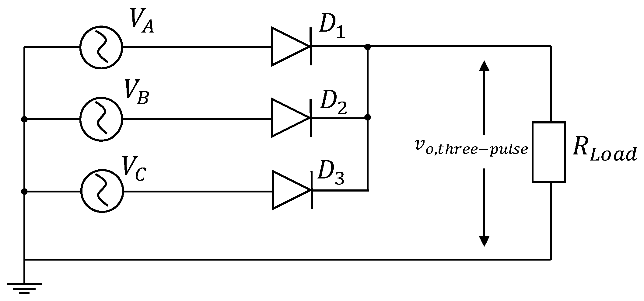
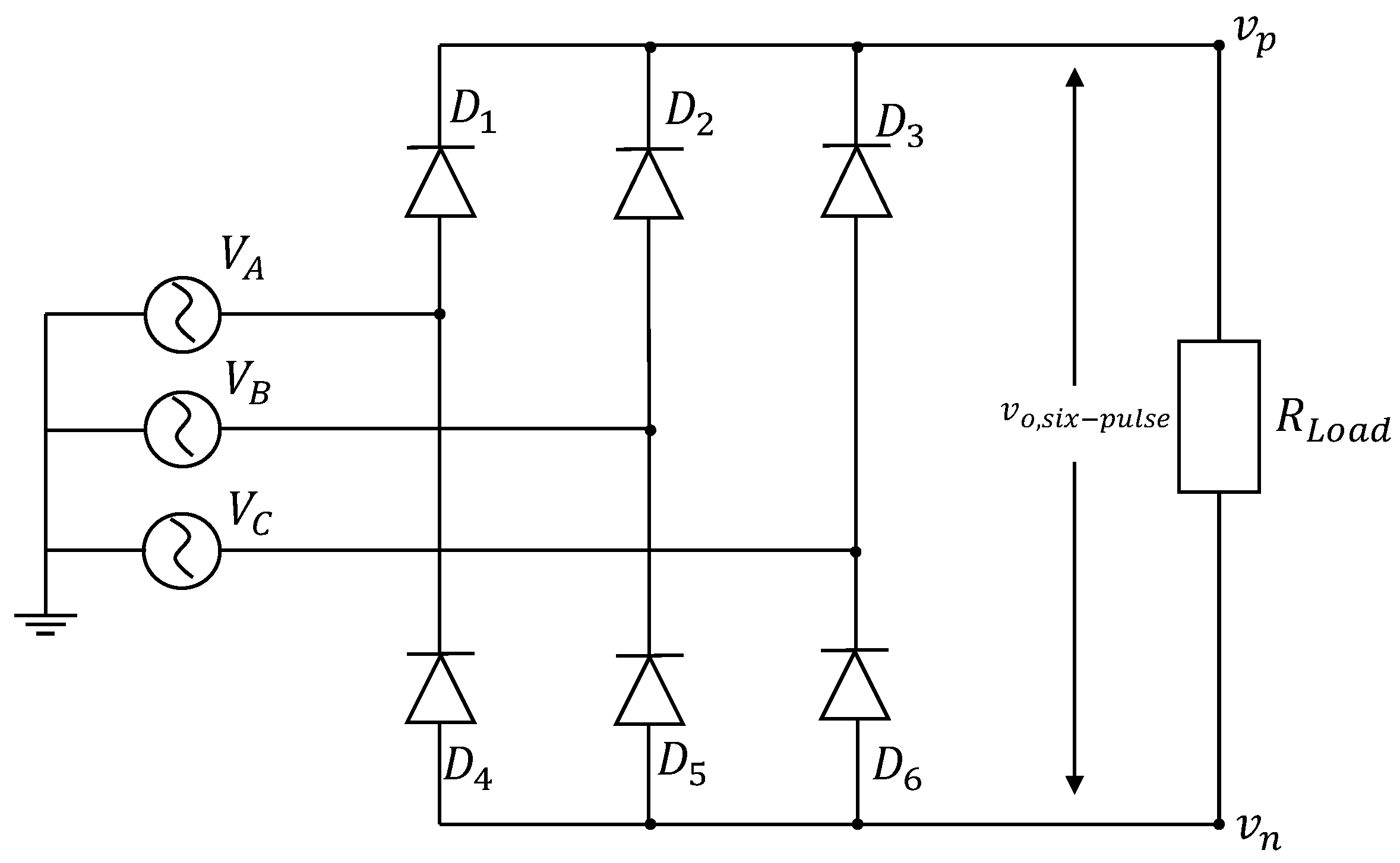
  27. Zhang, M.; Yuan, Y.; Sun, X.; Zhang, Y.; Li, X. Harmonic resonance suppression strategy of the front-end VIENNA rectifier in EV charging piles. IEEE Trans. Power Electron. 2022, 38, 1036–1053. [Google Scholar] [CrossRef]
  28. Lan, D.; Wu, Y.; Soeiro, T.B.; Granello, P.; Qin, Z.; Bauer, P. 12-pulse Rectifier with DC-Side Buck Converter for Electric Vehicle Fast Charging. In Proceedings of the IECON 2022–48th Annual Conference of the IEEE Industrial Electronics Society, Brussels, Belgium, 17–20 October 2022; IEEE: Piscataway, NJ, USA, 2022; pp. 1–6. [Google Scholar]
  29. Langella, R.; Testa, A.; Alii, E. IEEE recommended practice and requirements for harmonic control in electric power systems. In IEEE Recommended Practice; IEEE: Piscataway, NJ, USA, 2014. [Google Scholar]
  30. Abidin, M.N.Z. IEC 61000-3-2 Harmonics Standards Overview; Schaffner EMC Inc.: Edsion, NJ, USA, 2006. [Google Scholar]
  31. Kalpana, R.; Singh, B.; Bhuvaneswari, G. A 20-pulse asymmetric multiphase staggering autoconfigured transformer for power quality improvement. IEEE Trans. Power Electron. 2017, 33, 917–925. [Google Scholar]
  32. Liu, Z.; Meng, F.; Yang, W. Harmonic reduction technology at DC link in star-connected-autotransformer-based multi-pulse rectifier. In Proceedings of the 2017 IEEE Transportation Electrification Conference and Expo, Asia-Pacific (ITEC Asia-Pacific), Harbin, China, 7–10 August 2017; IEEE: Piscataway, NJ, USA, 2017; pp. 1–6. [Google Scholar]
  33. Meng, F.; Yang, W.; Zhu, Y.; Gao, L.; Yang, S. Load adaptability of active harmonic reduction for 12-pulse diode bridge rectifier with active interphase reactor. IEEE Trans. Power Electron. 2015, 30, 7170–7180. [Google Scholar] [CrossRef]
  34. IEEE 2030.1.1; Technical Specifications of Quick Charger for the Electric Vehicle. IEEE: Piscataway, NJ, USA, 2010.
  35. Qin, Z.; Tang, Y.; Loh, P.C.; Blaabjerg, F. Benchmark of AC and DC active power decoupling circuits for second-order harmonic mitigation in kilowatt-scale single-phase inverters. IEEE J. Emerg. Sel. Top. Power Electron. 2015, 4, 15–25. [Google Scholar] [CrossRef]
  36. Hu, H.; Harb, S.; Kutkut, N.; Batarseh, I.; Shen, Z.J. A review of power decoupling techniques for microinverters with three different decoupling capacitor locations in PV systems. IEEE Trans. Power Electron. 2012, 28, 2711–2726. [Google Scholar] [CrossRef]
  37. Qin, H.; Kimball, J.W. Closed-loop control of DC–DC dual-active-bridge converters driving single-phase inverters. IEEE Trans. Power Electron. 2013, 29, 1006–1017. [Google Scholar]
  38. Lahyani, A.; Venet, P.; Grellet, G.; Viverge, P.J. Failure prediction of electrolytic capacitors during operation of a switchmode power supply. IEEE Trans. Power Electron. 1998, 13, 1199–1207. [Google Scholar] [CrossRef]
  39. Karanayil, B.; Agelidis, V.G.; Pou, J. Performance evaluation of three-phase grid-connected photovoltaic inverters using electrolytic or polypropylene film capacitors. IEEE Trans. Sustain. Energy 2014, 5, 1297–1306. [Google Scholar] [CrossRef]
  40. Zhang, L.; Ruan, X. Control schemes for reducing second harmonic current in two-stage single-phase converter: An overview from DC-bus port-impedance characteristics. IEEE Trans. Power Electron. 2019, 34, 10341–10358. [Google Scholar] [CrossRef]
  41. Nguyen, D.D.; Bui, N.T.; Yukita, K. Design and optimization of three-phase dual-active-bridge converters for electric vehicle charging stations. Energies 2019, 13, 150. [Google Scholar] [CrossRef]
  42. Nguyen, D.D.; Pham, T.T.; Le, T.T.; Choi, S.; Yukita, K. A Modulation Method for Three-Phase Dual-Active-Bridge Converters in Battery Charging Applications. Sustainability 2023, 15, 5170. [Google Scholar] [CrossRef]
Figure 1. General system diagram.
Electronics 13 02527 g001
Figure 2. Three-pulse diode rectifier.
Electronics 13 02527 g002
Figure 3. Six-pulse diode rectifier.
Electronics 13 02527 g003
Figure 4. Fourier analysis of the six-pulse output voltage rectifier.
Electronics 13 02527 g004
Figure 5. DAB3 topology diagram.
Electronics 13 02527 g005
Figure 6. Some key waveforms of the DAB3 converter under SPS modulation.
Electronics 13 02527 g006
Figure 7. Bode plot of the resonance controller.
Electronics 13 02527 g007
Figure 8. Bode plot of the multi-resonance controller.
Electronics 13 02527 g008
Figure 9. The controller block diagram.
Electronics 13 02527 g009
Figure 10. Bode plot of the current loop under the conventional and proposed controllers.
Electronics 13 02527 g010
Figure 11. Zoom in of the Nyquist plot of the current loop with PI and R controller.
Electronics 13 02527 g011
Figure 12. Simulation results of the current and input voltage waveform in the scale down and high power. (a) Scale down 100 V/15 A without ripple-free technique. (b) Scale down 100 V/15 A with ripple-free technique. (c) High power at 355 V/50 A without ripple-free technique. (d) High power at 355 V/50 A with ripple-free technique.
Electronics 13 02527 g012
Figure 13. THD and PF survey under different power levels with the conventional and proposed methods. (a) THD analysis of the conventional and proposed methods under different loads. (b) PF analysis of the conventional and proposed methods under different loads.
Electronics 13 02527 g013
Figure 14. Prototype of the DAB3 converter [42].
Electronics 13 02527 g014
Figure 15. The 100 V/15 A scale down experiment results. (a) The result of ramping up current at the start-up without ripple-free technique. (b) The results of ramping up current at the start-up with ripple-free technique. (c) The result at the steady steady state waveforms without ripple-free technique. (d) The result at the steady state waveforms with ripple-free technique. (e) The AC coupling of the voltage and current ripple without ripple-free technique. (f) The AC coupling of the voltage and current ripple with ripple-free technique.
Electronics 13 02527 g015
Table 1. Limit value of the current ripple following the CHAdeMO standard.
FrequencyLimit Value (Ap-p)
10 Hz or less1.5
5 kHz or less3.0
150 kHz or less9.0
Table 2. Some key parameters for designing the controller and simulation.
ParametersSymbolsValue
Input and output Voltage V 1 and V 2 100 V
Transformer turn ration1:1
Leakage inductance L k 12.5 μ H
Magnetizing inductance L m 0.9 mH
Input and output filter capacitor C o u t 250 μ F
Switching frequency f s 50 kHz
Table 3. The key parameters of the DAB3 converter.
ParametersSymbolValue
Input voltage V 1 100 V
Output voltage V 2 100 V
Power P o u t 1.5 kW
Frequency f s 50 kHz
Turn ration1 (7:7)
Magnetizing inductance L m 0.9 mH
Leakage inductance L k 12.5  μ H
Wire Lizt 1050AWG38
Core EE42/21/15 (N87)
Disclaimer/Publisher’s Note: The statements, opinions and data contained in all publications are solely those of the individual author(s) and contributor(s) and not of MDPI and/or the editor(s). MDPI and/or the editor(s) disclaim responsibility for any injury to people or property resulting from any ideas, methods, instructions or products referred to in the content.

