Article

Inkjet-Printed Reflectarray Antenna Integrating Feed and Aperture on a Flexible Substrate Using Origami Techniques

Department of Electronic Engineering, National Taipei University of Technology, 1, Sec. 3, Zhongxiao E. Rd., Taipei 10608, Taiwan
*
Author to whom correspondence should be addressed.
Electronics 2024, 13(13), 2505; https://doi.org/10.3390/electronics13132505
Submission received: 12 May 2024 / Revised: 21 June 2024 / Accepted: 24 June 2024 / Published: 26 June 2024

Abstract

This paper presents an innovative method for fabricating reflectarray antennas using inkjet printing technology on flexible substrates, markedly enhancing integration and manufacturability compared to traditional PCB methods. The technique employs inkjet printing to deposit conductive inks directly onto a flexible polyethylene naphthalate (PEN) substrate, seamlessly integrating feed and reflectarray components without complex assembly processes. This streamlined approach not only reduces manufacturing complexity and costs but also improves mechanical flexibility, making it ideal for applications requiring deployable antennas. The design process includes an origami-inspired folding of the substrate to achieve the desired three-dimensional antenna structures, optimizing the focal length to dimension ratio (F/D) to ensure maximum efficiency and performance. The feed and the reflectarray geometry are optimized for an F/D of 0.6, which achieves high gain and aperture efficiency, demonstrated through detailed simulations and measurements. For normal incidence, the configuration achieves a peak gain of 9.3 dBi and 48% radiation efficiency at 10 GHz; for oblique incidence, it achieves 7.3 dBi and 40% efficiency. The study underscores the significant potential of inkjet-printed antennas in terms of cost-efficiency, precision, and versatility, paving the way for new advancements in antenna technology with a substantial impact on future communication systems.

1. Introduction

Reflectarray antennas are increasingly pivotal in modern communication systems, offering a sophisticated alternative to traditional parabolic reflectors. The innovation of reflectarrays lies in their ability to use printed circuit board (PCB) technology to achieve high antenna gain, leveraging flat, easily manufactured unit cells in place of complex, curved surfaces. This approach significantly simplifies fabrication processes while achieving or surpassing the performance of conventional designs. Reflectarrays are distinguished by their efficient manufacturability and their capacity for high precision in directing electromagnetic waves, which has led to diverse fabrication methodologies aimed at enhancing performance, reducing costs, and facilitating easier integration with other components.
However, the integration of the feed with the reflectarray surface still represents a substantial challenge in antenna design. Conventional methods typically require auxiliary fixtures to align the feed at the focal point, complicating the manufacturing process and detracting from the efficiency advantages of PCB technology. This additional complexity highlights a crucial hurdle: achieving a seamless integration of feed and reflectarray in a manner that preserves the manufacturing simplicity and cost-effectiveness intrinsic to reflectarray technology. The necessity for external supports or complex assembly processes underscores the need for innovative approaches that can simplify antenna construction without sacrificing performance.
This paper proposes a distinctive method that integrates the feed and reflectarray aperture onto a single flexible substrate, utilizing inkjet-printed technology for fabrication. This approach eliminates the need for separate assembly processes or additional structural components, significantly simplifying the alignment of the feed and reflectarray. It also reduces the overall manufacturing complexity and cost. By fabricating both the feed and reflectarray on the same substrate, this method also enhances mechanical robustness and facilitates easier deployment, particularly in applications requiring flexible or conformable antenna solutions. The integration of the feed and reflectarray into a coherent unit manufactured via inkjet printing on a flexible substrate represents a significant advancement in antenna design, offering a streamlined, cost-effective pathway to high-performance antenna systems.
The literature reveals incremental advancements in reflectarray technology, including efforts to utilize inkjet printing for antenna fabrication, explore flexible substrates for enhanced mechanical versatility, and apply origami principles for deployable structures [1,2,3,4,5,6,7]. However, existing studies typically address these aspects in isolation, focusing on either the manufacturing technique, the substrate material, or the deployment mechanism without fully integrating these components into a singular, cohesive design. While inkjet printing has been explored for its potential in patterning conductive materials on substrates, its application in creating comprehensive antenna systems, including both the reflectarray and feed mechanism, remains underexplored. Similarly, the use of flexible substrates has primarily been investigated in the context of conformable or wearable technologies [8,9,10,11,12,13], with less emphasis on the integration of flexible manufacturing processes with high-performance antenna designs. Origami-inspired antennas have demonstrated potential in deployability [14,15,16,17,18] and mechanical reconfigurability [19,20,21], yet the seamless integration of origami principles with advanced manufacturing techniques and materials science to produce fully integrated, high-efficiency reflectarray systems has not been comprehensively achieved. Unlike previous work that integrated aperture and feed elements on flexible substrates using PCB techniques [22], this paper introduces the novel application of inkjet printing to achieve the same integration, which enhances design versatility and significantly reduces manufacturing complexities and costs. More specifically, inkjet printing reduces material and labor costs as it is an additive manufacturing method. In terms of time efficiency, the printing process is faster and more streamlined compared to traditional PCB fabrication and assembly. Finally, considering design flexibility, inkjet printing allows for more versatile and precise deposition of conductive inks, enabling complex and customized designs on flexible substrates. Thus, this study builds upon yet significantly advances the concepts introduced earlier.
In particular, inkjet printing shows distinct features as compared to other electronic printing methods such as aerosol jet printing (AJP), direct ink writing (DIW), and electrohydrodynamic printing (EHD). AJP can print finer features with higher resolution than inkjet printing. However, it requires more complex equipment and higher operational costs. Inkjet printing is more accessible and cost-effective, making it suitable for rapid prototyping and low-to-medium volume production. DIW offers the ability to print highly viscous materials and create three-dimensional (3D) structures. However, it lacks the high resolution and speed of inkjet printing. For applications requiring detailed patterns on flexible substrates, inkjet printing provides better performance. EHD can achieve extremely high resolution, but it involves complex setups and is limited by slower printing speeds. Inkjet printing strikes a balance between resolution, speed, and cost, making it ideal for producing flexible electronic components like antennas. Thus, inkjet printing is pursued in this research due to its balance of precision, cost-effectiveness, and suitability for flexible substrates, offering significant advancements in the design and fabrication of high-performance reflectarray antennas.
In demonstrating the proposed concept, this study focuses on designing and fabricating specific structures that validate the integrated feed and reflectarray approach. By employing a flexible polyethylene naphthalate (PEN) substrate, the paper delineates the process of inkjet printing conductive patterns to form the reflectarray and feed elements, followed by the origami-inspired folding of the substrate to assemble the 3D antenna structure. The examination includes detailed performance metrics, such as gain, efficiency, and beam pattern, comparing these results with traditional antenna designs to underscore the advantages of the proposed method. This empirical validation not only proves the feasibility of the concept but also establishes a foundation for future research and development in integrated antenna systems, offering a clear, tangible pathway toward more efficient, cost-effective, and versatile antenna technologies.

2. Fabrication Process

2.1. Inkjet Printing

Before demonstrating the design and manufacturing of the proposed reflectarrays, we first explain the inkjet-printed process used in this study [23]. The inkjet-printed process is performed through the FUJIFILM Dimatix 2850 nanoparticle inkjet printer (DMP-2850). Its components include an ink cartridge, a cleaning pad for nozzle clogging, a printing platform, and cameras for droplet observation and positioning.
The printer has two nozzle systems: a single-nozzle system and a multi-nozzle system. The single-nozzle system operates by moving the printing platform in the x–y direction to inkjet the required pattern, where the droplet spacing and position are also determined by the movement of the platform. The multi-nozzle system arranges all nozzles in a row, operating at an angled cartridge, where the printhead movement along the substrate determines the x–spacing and the angle determines the y–spacing of the droplets. The DMP-2850 has the advantage of being compatible with ink cartridges that can use multiple nozzles at once, and current models on the market have up to 16 nozzles, effectively reducing printing time and avoiding nozzle clogging issues.
The inkjet printing process begins with exporting the finalized antenna design file to the pattern editing software, such as ACE-3000 used in this study, where it undergoes file conversion. Before initiating the printing, the conductive ink is loaded into the ink cartridge in a single-fill operation, with a maximum ink volume of 1.5 ml. The cartridge and a cleaning pad are then installed into the printer. The DMP-2850 operation primarily involves two components: the Droplet Watcher and the Fiducial Camera. The Droplet Watcher is tasked with calibrating and cleaning nozzles 1 to 16, verifying nozzle conditions within the cartridge, and selecting the nozzle number for printing.
The waveform used for ink droplet ejection in the FUJIFILM Dimatix DMP-2850 inkjet printer is critical for controlling droplet formation and ensuring consistent ejection. The optimization of these waveform parameters was undertaken to achieve control over droplet size and ejection consistency, which is essential for high-quality printing. Initially, standard settings provided by the manufacturer were used to establish a baseline. The jetting voltage was then varied to control droplet velocity and size. Higher voltages increase droplet speed, but if set too high, they can cause satellite droplets, leading to print defects. The optimal jetting voltage was determined to be 30.5 V, which balanced droplet formation and minimized defects. The pulse frequency and shape were also adjusted to optimize droplet breakup and ensure uniformity. The pulse frequency was set to 5 kHz, which was found to provide a balance between droplet formation and ejection speed. Using the Droplet Watcher system, the droplet formation was observed in real-time, allowing for adjustments to the waveform shape and duration. This real-time observation ensured consistent droplet size and minimized any satellite droplets. Finally, the optimized settings for the waveform included a specific pulse shape tailored to the viscosity and surface tension of the ink. These settings ensured stable and consistent droplet formation, which was critical for achieving high-quality and high-resolution prints.
Prior to placing the substrate on the printing platform, it is essential to test the surface tension of the substrate to ensure compatibility between the conductor ink and the substrate. Once the substrate is positioned on the platform, a vacuum is activated to secure it in place. For substrates less than 0.5 mm thick, the platform can accommodate a maximum printing area of 210 × 315 mm2; substrates between 0.5 and 25 mm thick are limited to a maximum area of 210 × 260 mm2. The Fiducial Camera then performs a calibration of the substrate and printing points, covering an observation range of 1.62 × 1.22 mm2 and a resolution of 2.54 μm/pixel.
After the printing is complete, the substrate with the printed conductor ink patterns is immediately transferred to a hot air circulating oven for curing. This study employs the SIGMA BS400 oven, which can be temperature-adjusted up to 200 °C. The oven is equipped with an electronic temperature controller, an over-temperature controller, an ammeter, and an electric heating switch. Prior to usage, the external power main and the exhaust system are activated. The over-temperature controller is then adjusted to the rated temperature to prevent overheating inside the oven. Subsequently, the power and startup switches are turned on, and the required baking temperature is set using the displacement and up/down keys on the electronic temperature controller. The SV display indicates the currently set temperature, while the PV display shows the internal oven temperature. More specifically, the post-heat treatment process was performed to ensure the reliability and performance of the inkjet-printed reflectarray. The printed substrates were initially baked at a temperature of 200 °C for 30 minutes. However, to address issues such as the coffee ring effect caused by rapid evaporation of the ink at the edges, a sequential temperature increase method was adopted. This method involved baking the substrates at progressively higher temperatures to improve the uniformity and conductivity of the printed patterns. The curing process was conducted in seven stages, with each stage involving a different temperature and duration to achieve optimal results. The stages started with baking at 30 °C and were terminated by baking at 200 °C. This gradual temperature increase ensured that the ink particles properly coalesced, significantly improving the surface uniformity and conductivity of the printed patterns. Finally, the baking process completed the inkjet printing process.

2.2. Material Properties

After describing the inkjet printing process, this study analyzes the material characteristics of the substrate and conductors before proceeding with the antenna design. Furthermore, these material characteristics complement the inkjet printing process, necessitating corresponding baking, coating, and substrate selection to complete the set material characteristics.
Initially, the study analyzes the properties of conductors. Conductive ink is an indispensable part of the inkjet printing process as the ink distributed from the nozzles forms droplet characteristics on the substrate such as viscosity, surface tension, thermal performance, and substrate compatibility. These factors are crucial for the designed printing process. Common conductive inks used in inkjet printing include polymer-based and metal nanoparticle inks, with nanoparticle inks recently being widely used to achieve high-frequency conductive structures on organic or composite substrates.
This research utilizes silver-based nanoparticle ink. More specifically, the ink employed is the DGP 40LT-15C, sourced from FUJIFILM Dimatix. This silver nanoparticle ink is chosen due to its high conductivity of 9.1 × 10⁶ S/m and low curing temperature of 120 °C. These properties make it ideal for low-temperature substrates such as paper, polyethylene terephthalate (PET), and polymers. Specifically, the use of dyne pens to measure surface tension, which directly correlates with the adhesion properties of the substrate, has been conducted. The test method involves drawing a line on the surface of the substrate with the ink from the dyne pen, which quickly reveals the surface tension and wettability of the substrate. Surface tension is related to the wetting angle, which is the angle at which the ink droplet contacts the substrate. This angle can indicate whether the surface is hydrophilic or hydrophobic. If the wetting angle is too large, the ink droplet will form a spherical shape on the substrate; if the wetting angle is too small, the ink droplet will spread out, affecting conductivity. By changing the dyne level of the test pens until the ink line remains unshrunk, we determine the adhesion strength of the substrate. If the ink line on the substrate does not form any droplets within two seconds, it indicates that the surface tension of the substrate is greater than or equal to the dyne level of the pen, which is a hydrophilic phenomenon, showing that the ink adheres well to the substrate. If the ink line slowly shrinks, it indicates that the surface tension of the substrate is less than the dyne level of the pen. If the ink line immediately shrinks and forms droplets, it indicates that the surface tension of the substrate is much lower than the dyne level of the pen, which is a hydrophobic phenomenon, showing that the ink does not adhere well to the substrate. Our results showed that the surface tension of the PEN substrate is approximately 30–32 dyn/cm. The surface tension of the conductive ink used in this study is about 37 dyn/cm, indicating that the surface tension of the substrate is not significantly lower than that of the conductive ink. This result demonstrates good compatibility between the substrate and the ink, confirming the adhesion strength of the selected materials. Since the ink deposited on the substrate is not a continuous conductor but rather closely spaced silver particles, this indicates its low conductivity. Thus, it is necessary to heat the conductor ink and melt the nanoparticles together to achieve high conductivity. Some studies have used methods like thermal curing, laser curing, and ultraviolet irradiation to cure the ink. However, variables such as ink viscosity, surface tension, number of printing layers, oven curing temperature, and time all affect its conductivity, meaning that the ink has different conductivities in its liquid and solid states. Therefore, this paper uses thermal curing to solidify the conductor ink and achieve the optimal settings for a higher conductivity structure.
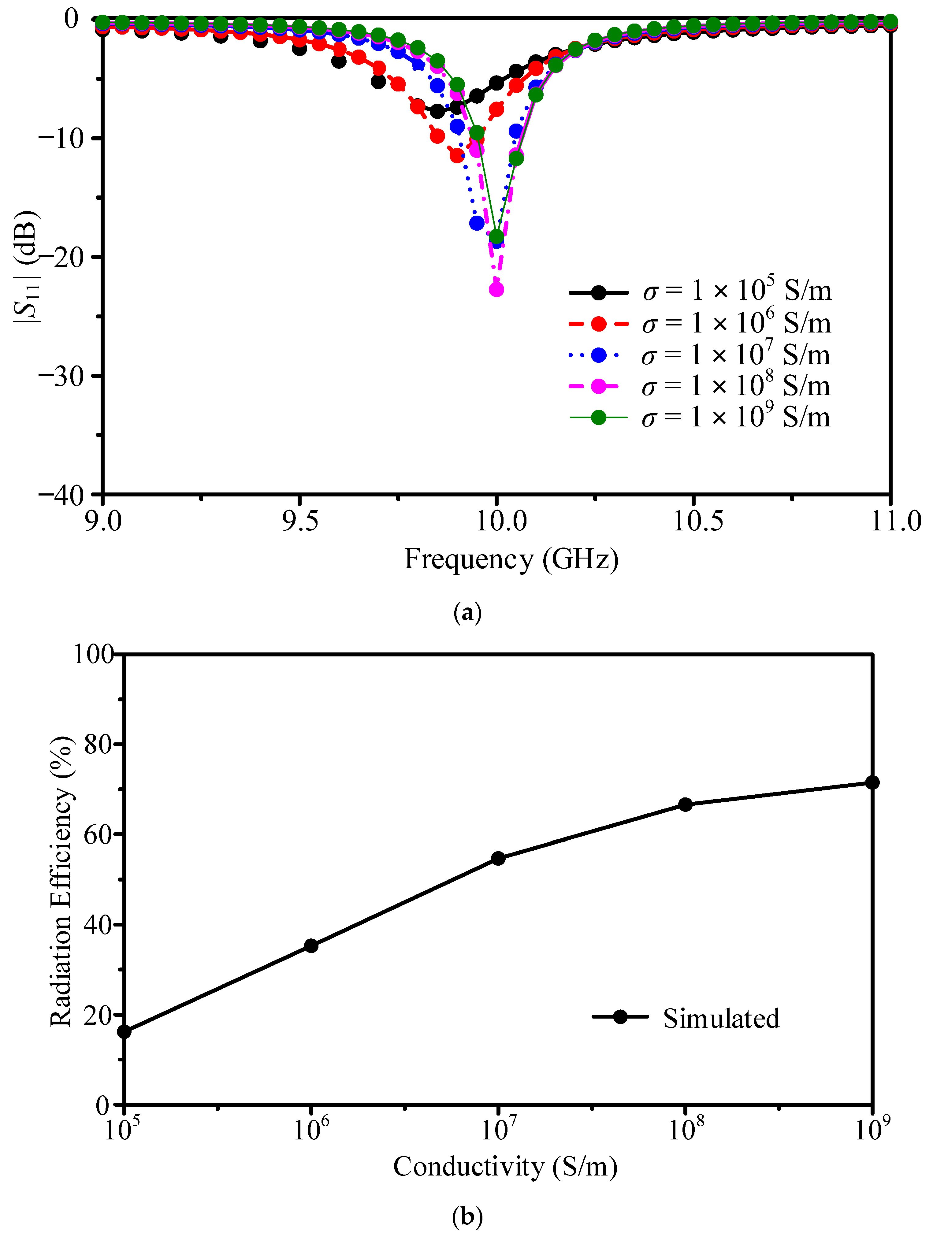
To characterize the conductivity of the printed conductor layers, this study first predicts the impact of conductivity on the impedance matching of a microstrip antenna. While the detailed structure of the microstrip antenna will be detailed in the next section, this section analyzes the effect of the conductivity on the antenna performance. The conductivity, denoted by σ, is adjusted from 1 × 10⁵ to 1 × 10⁹ S/m, which affects the impedance matching as shown in 
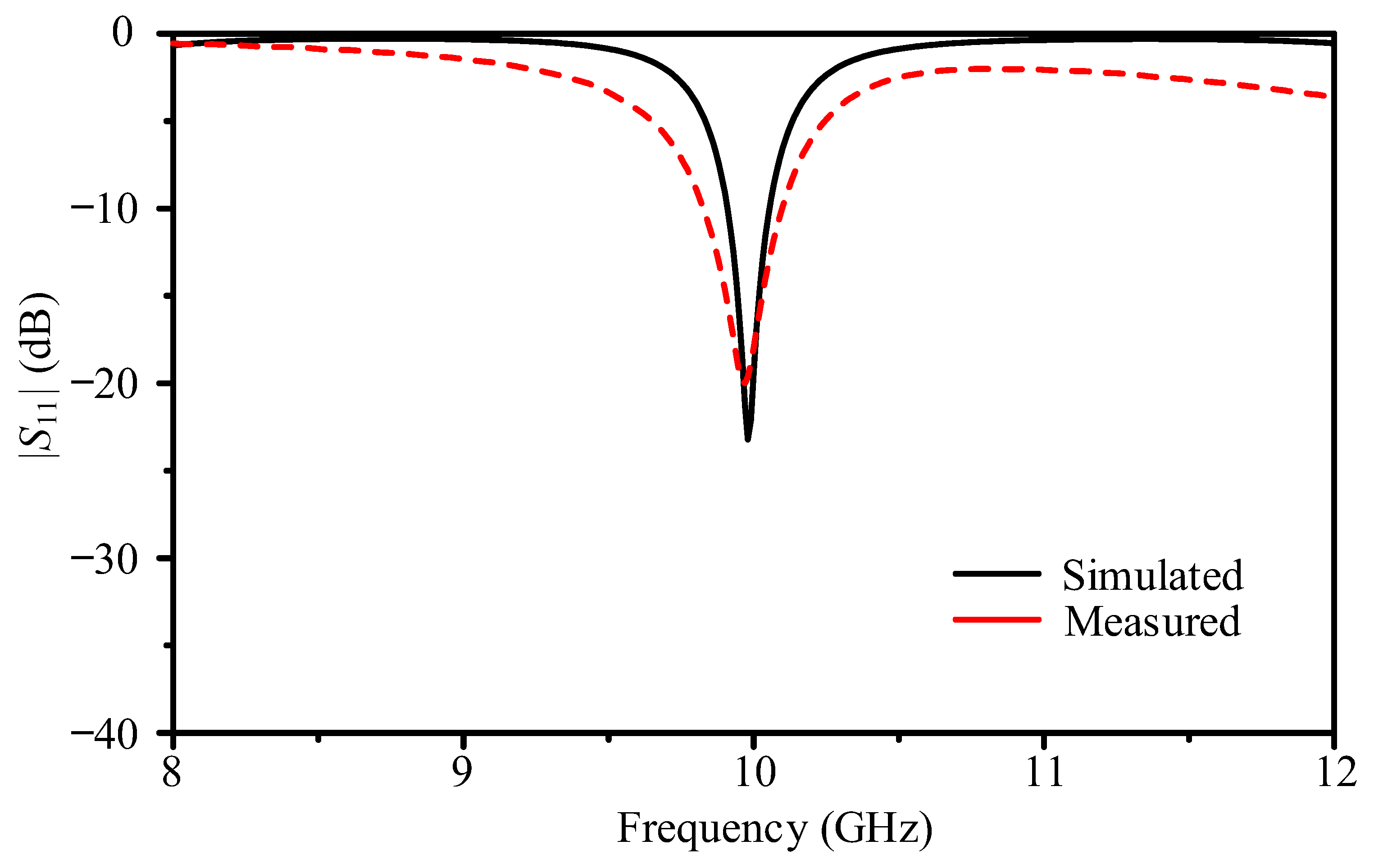
Figure 1a. When σ is lower, it can be observed that the resonance frequency shifts to a lower frequency, causing poor antenna matching. Figure 1b shows the radiation efficiency of the antenna at 10 GHz, illustrating that the conductivity significantly affects its efficiency. With a conductor conductivity of 1 × 10⁵ S/m, the radiation efficiency is only 16%, indicating poor conductivity of the antenna, which also affects the radiation efficiency and gain. However, based on the above observations, it is known that by increasing the number of printed ink layers, curing temperature, and time, the conductivity can be increased. As a result, this study designs an antenna printed with three layers of conductor. This indicates that the conductivity of the printed three layers of conductor is approximately in the range of 1 × 10⁵ to 1 × 10⁷ S/m, and the optimum radiation efficiency is about 55%.
The sintering process for the DGP 40LT-15C silver nanoparticle ink used in our study involves a thermal curing method. Given that PEN has a glass transition temperature (Tg) of 120 °C, the sintering temperature for the silver nanoparticle ink was selected to align with this constraint. The sintering process was conducted at 110 °C for 1 h to ensure effective curing of the ink while preventing any deformation or damage to the PEN substrate. This temperature is slightly below the Tg of PEN, ensuring the structural integrity of the substrate while achieving optimal electrical conductivity of the printed film. Additionally, maintaining the sintering temperature just below Tg prevents issues like warping or changes in the physical properties of the PEN substrate, which could affect the overall performance and reliability of the antenna. This consideration ensures the final product maintains both structural integrity and high functionality. Additionally, to address the coffee ring effect and ensure uniform ink distribution, the curing process was performed in a hot air circulating oven with a controlled temperature ramp. The gradual increase in temperature helps to avoid rapid solvent evaporation, which can cause uneven ink distribution and affect the quality of the printed patterns. The resultant film thickness of the printed conductor on the PEN substrate, after three layers of printing, was measured to be 25 μm. This was determined using a scanning electron microscope (SEM). An example of the SEM image is shown in Figure 2a, which indicates the 3-layer cross-sectional profile for the depositions. By measuring the thickness at the 10 sample points, the resultant film thickness of the printed conductor on the PEN substrate, after three layers of printing, can be determined. Similarly, another example is the 1-layer of printing, as shown in Figure 2b. The final thickness was determined by the average, which was found to be 10 μm on different substrates.
Next, we examined the material characteristics of dielectric substrates utilized in the design of a reflectarray. Specifically, we analyzed flexible substrates such as PET, PEN, and polyimide (PI), focusing on how their thickness impacts the adjustable phase range of reflectarray unit cells. Generally, thicker substrates offer a larger adjustable phase range, though this comes with increased loss. A key feature of the proposed technique is the ability to conveniently increase the board thickness by folding flexible substrates. We varied the thicknesses of PET, PEN, and PI to simulate their adjustable phases, as presented in Figure 3. The results demonstrate that PEN, in particular, provides superior phase adjustability with increasing thickness compared to PET and PI, making it the optimal choice for subsequent antenna designs. This is illustrated in Figure 3, where the simulated results show a steep increase in the adjustable phase range for PEN, compared to the more moderate improvements seen with PET and PI. This capability to adjust phase effectively by altering substrate thickness is crucial for optimizing antenna performance while minimizing losses, solidifying PEN as the substrate of choice in the development of advanced antenna structures.
More specifically, the PEN utilized is sourced from Goodfellow Corporation. The surface free energy of PEN is measured to be approximately 42.8 dyn/cm, which ensures good wettability and adhesion with the conductive ink used in the inkjet printing process. Additionally, the surface roughness of the PEN substrate was characterized using atomic force microscopy (AFM), revealing an average roughness of 2.3 nm. In particular, the initial layer of ink is deposited on the PEN substrate, and its interaction is primarily governed by the surface energy of the substrate and the surface tension of the ink. The ink had a lower surface tension than the critical surface tension of the PEN substrate to achieve proper wetting and adhesion. The contact angle measurement indicated a favorable wetting behavior, crucial for forming a uniform initial layer. For subsequent layers, the interaction changes as the ink is deposited on a layer of previously deposited ink. The critical factors here include ink penetration and merging, layer homogeneity, and sintering effects. The process starts by ensuring that new ink droplets merge seamlessly with the underlying layer to avoid delamination. The controlled print speed and droplet spacing facilitate uniform droplet merging. Afterwards, the uniformity of the underlying layer was maintained by optimizing the droplet spacing (30 μm), providing consistent overlap and coverage. Sintered layers can have different surface roughness, impacting wetting behavior. The sintering process aims to achieve a smooth and uniform surface, enhancing the adhesion of subsequent layers.

2.3. Parametric Effects

To clarify the parameters of inkjet printing, the ink’s rheological properties and kinematic settings were further analyzed. The kinematic settings of the FUJIFILM Dimatix DMP-2850 printer were carefully optimized to achieve high-quality prints. The printer’s multi-nozzle system allowed for precise control over droplet spacing, set at 30 μm, which balanced the need for high resolution and uniform deposition. This careful control helped mitigate issues such as the coffee ring effect, where ink accumulates at the edges of printed patterns, leading to non-uniform conductivity. By maintaining these precise settings, we ensured the production of a consistent and high-performance conductive layer necessary for the functionality of the reflectarray.
Moreover, the printing speed was set at 10 mm/s, providing adequate control over the deposition process. This speed was selected to prevent defects such as splattering or insufficient coverage while maintaining high throughput. The layer thickness achieved per pass was approximately 1.2 µm, optimized to ensure electrical performance while maintaining the flexibility of the substrate. Multiple layers were printed to achieve the desired thickness. The curing temperature and time are crucial for achieving the desired electrical properties of the printed ink. For PI substrates, the printed patterns were cured at 150 °C for 30 minutes; nevertheless, for substrates with lower Tg, such as PEN and PET, the curing temperatures were set below their respective Tg values to ensure mechanical integrity. Specifically, curing was conducted below 120 °C for PEN and below 75 °C for PET substrates. In practical terms, the antenna is suitable for use in a variety of applications, including wearable electronics, flexible sensors, and other devices operating within the temperature range of –40 °C to 115 °C. For applications requiring operation above 120 °C, alternative substrate materials with higher Tg values may be considered to ensure durability and performance.
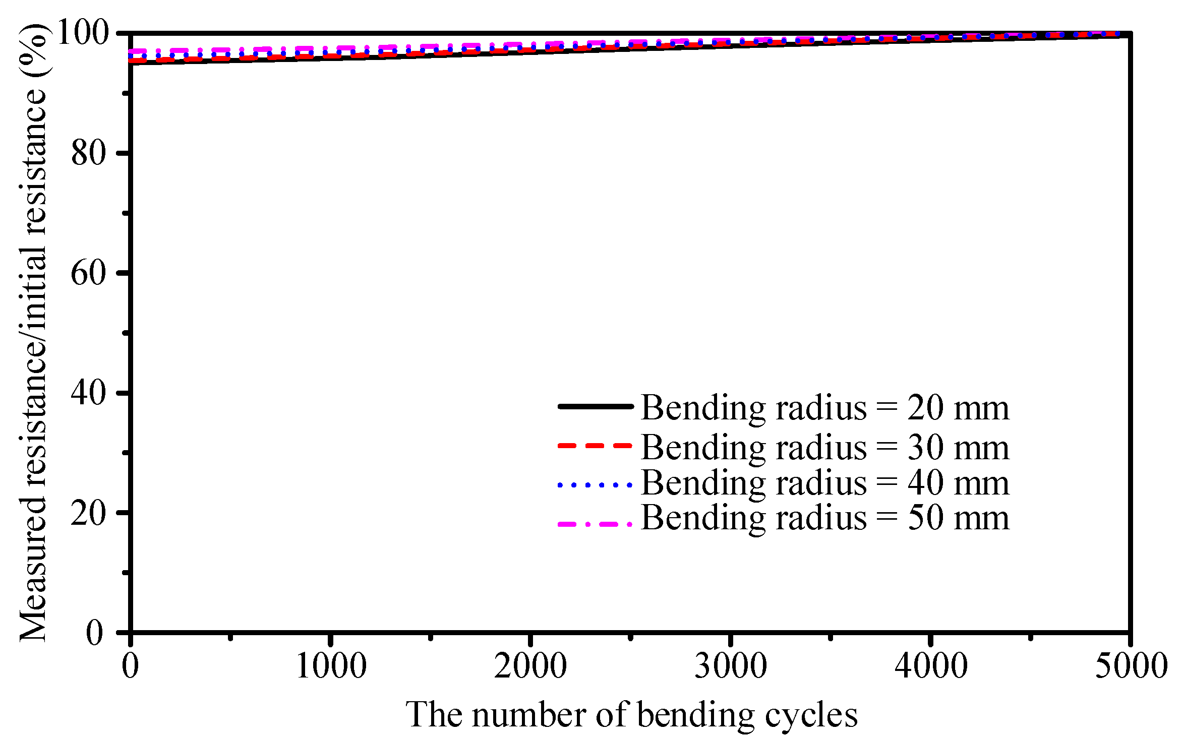
In addition, to ensure the reliability and durability of the printed antenna, we conducted bending tests to assess the relative resistance change under mechanical stress. In our experiments, the relative resistance change of the inkjet-printed silver nanoparticle traces on the PEN substrate was measured after multiple bending cycles. The specimens, sized 60 mm × 60 mm, were subjected to repeated bending with radii of 20 mm, 30 mm, 40 mm, and 50 mm using polystyrene fixtures. The initial resistance was recorded using a multimeter, followed by resistance measurements after every 1000 bending cycles. The measured results are shown in Figure 4. Our results showed that after 5000 bending cycles, the relative resistance change was less than 5%, indicating excellent mechanical durability and reliability of the printed antenna.
In addition to using dyne pens to assess the surface tension of the PEN substrate, we conducted a Scotch tape test to evaluate the adhesion strength of the inkjet-printed electrodes [24]. The test involved applying Scotch tape to the printed electrodes and subjecting the samples to multiple peeling cycles (5, 10, 30, and 50 cycles). Visual inspection after each set of cycles revealed no delamination or damage. Furthermore, the relative resistance change was measured to be less than 2% after 50 peeling cycles, indicating strong adhesion and minimal impact on electrical performance.
These detailed considerations of ink rheological properties, kinematic settings, and bending durability underscore the robustness of our inkjet printing methodology and highlight the innovative aspects of our approach in integrating both feed and aperture elements onto a single flexible substrate.

3. Inkjet-Printed Reflectarray with Normal Incidence

Section 3 and Section 4 of this paper are dedicated to demonstrating the implementation of reflectarray antennas with normal and oblique incidence feeds, respectively, building upon the foundational methodologies established in Section 2. The logical progression from the fabrication techniques detailed previously into practical antenna applications underscores the versatility and potential of inkjet-printed, flexible substrates in advanced antenna designs. Section 3, in particular, focuses on detailing the geometric structuring and integration of feed elements and reflectarrays into a single flexible substrate, advancing from mere component fabrication to functional antenna assembly. This approach aims to overcome the traditional challenges associated with the manufacturing and alignment sensitivities of conventional reflectarray antennas by proposing and demonstrating a novel technique of folding the flexible substrate into predetermined 3D shapes.
Illustrating these concepts, Figure 5 showcases the unfold and 3D structure of the reflectarray antenna within a hexahedral framework. This visualization provides the antenna geometry and highlights the practical application of the folding and unfolding mechanisms in tailoring antenna characteristics to specific requirements. The presented designs of polyhedral structures, specifically a hexahedron and a tetrahedron, exemplify this integrated approach. These configurations are optimized based on theoretical designs that dictate the focal length, denoted by F, and dimensions, denoted by D, of the reflectarray (with an optimal F/D of 0.6 for maximum efficiency), thus ensuring the practical efficacy of the antenna in real-world applications.

3.1. Feed Antenna

As a proof of concept, the proposed inkjet-printed origami reflectarray is designed at 10 GHz. The substrate material is polyethylene naphthalate (PEN) with a dielectric constant of 3.43 and a loss tangent of 0.005, with a thickness of 0.25 mm. Figure 6 shows the detailed feed antenna structure. This patch antenna is designed and optimized with parameters such as the patch width (Wpa = 10.8 mm), length (Lpa = 7.85 mm), and ground dimensions (Wgnd = Lgnd = 20 mm). The patch antenna is fed at the corner, which typically can be associated with attempts to achieve circular polarization. However, in this particular design, the corner feeding is employed primarily for impedance matching purposes. Based on the radiation patterns, which will be shown as follows, the antenna remains linearly polarized.
The feed antenna is simulated and measured. Figure 7 illustrates the reflection coefficient across 8–12 GHz, while Figure 8 displays the peak gain. The simulated impedance bandwidth, characterized by a reflection coefficient less than –10 dB, is observed to be 1.6%. This narrow bandwidth is typical for microstrip patch antennas, reflecting their inherent limitation in bandwidth capacity due to the high Q factor of the resonant structure. The measurements closely aligned with the simulated results, showcasing a reflection coefficient of –18 dB at 10 GHz and revealing a slightly broader actual bandwidth percentage of 2.6%. The peak gain of 4.9 dBi is observed at 9.98 GHz—closely matching the targeted 10 GHz operation. Additionally, Figure 9 shows the radiation patterns in the E-plane and H-plane, demonstrating a front-to-back ratio (FBR) of 17.1 dB and a cross-polarization discrimination (XPD) of 24.8 dB. The half-power beamwidths (HPBW) are 80.6° and 74.7° in the E-plane and H-plane, respectively. The measured cross-polarization level is higher than the simulated one in Figure 9 due to several factors related to the experimental setup and the inherent limitations of practical measurements; nevertheless, the radiation performance indicates a directed beam, suitable for serving the reflectarray as a feed.
In the design of the reflectarray antenna, the radiation pattern of the feed antenna plays a crucial role in determining the optimal F/D. For effective design integration, the feed pattern was approximated by the function cosqθ, where q is an exponent that aligns with the characteristics of the pattern. It was identified that when q = 2.8 the cosqθ pattern closely aligns with the simulated radiation patterns of the E-plane and H-plane. Integrating this value of q into the analyses for illumination efficiency and spillover efficiency, the overall antenna efficiency was computed [25]. The findings indicated that an F/D of 0.6 yields the highest overall efficiency, evaluated as 59%. This efficiency benchmark guided the structural design of the antenna, culminating in the 3D architecture shown in Figure 5.

3.2. Reflectarray Antenna

Next, the unit cells of the reflectarray were designed to achieve a full phase adjustable range, essential for beam steering. Five distinct unit cell shapes were considered: rectangular, circular, square-ring, circular-ring, and cross-shaped, optimized for a target frequency of 10 GHz on the PEN substrate. The substrate thickness was set at 0.5 mm to balance phase resolution and minimize physical size. Among the configurations, the square-ring unit cell exhibited superior performance, achieving a phase adjustable range up to 343° with a loss of 2.91 dB, demonstrating its effectiveness in providing extensive phase control with minimal loss. The simulated insertion loss of 2.91 dB in the reflectarray element is primarily caused by a combination of factors, including the properties of the substrate and the conductivity of the printed conductor layer. The flexible PEN substrate, while chosen for its mechanical and thermal properties, does introduce some dielectric loss. However, the more significant contributor to the insertion loss is the lower conductivity of the printed silver nanoparticle ink compared to bulk metal conductors. Additionally, the multi-layer printing process, while improving the thickness and overall conductivity of the printed traces, cannot entirely mitigate the inherent losses associated with the lower conductivity of the printed ink. The unit cell spacing was maintained at a 0.22 wavelength to reduce mutual coupling while conserving array compactness.
Figure 10 demonstrates the profile of the unit cell. This configuration leveraged a multi-layer stacking approach, using a minimal gap of 0.01 mm between layers. Such a multi-layer structure can be efficiently created, as the proposed technique can fold a planar substrate into a 3D and multi-layer configuration. This method effectively utilized the substrate characteristics and the geometrical flexibility of the unit cells to meet the design requirements for high-performance beam steering in reflectarray applications.
In the design of the reflectarray, the phase distribution across the aperture is critical for achieving in-phase radiation from all unit cells. By employing the square-ring unit cell sizes, the reflectarray is configured to cover a full 360° adjustable phase range, which allows for fine-tuning the phase of each unit cell to achieve a coherent wavefront.
Specifically, the reflectarray utilizes eight different square-ring unit cell structures, arranged to incrementally cover the required phase range with each unit providing a distinct phase shift. This setup ensures that the phase shift between adjacent cells increments by 45. This arrangement is chosen to ensure a phase progression across the reflectarray, facilitating uniform wavefront shaping and maintaining high directivity.
Each unit cell is positioned within the reflectarray aperture, measuring 99 × 99 mm2, composed of 15 × 15 unit cells, to match the design criterion of F/D = 0.6. The layout of the unit cells is such that the transitions between the phase states are smooth, minimizing discontinuities and ensuring that the reflectarray can effectively focus the radiated energy. Figure 11 shows the arrangement of the unit cells, which allows the reflectarray to perform with enhanced gain and efficiency.
Finally, the reflectarray aperture is created using inkjet printing techniques, which facilitates the placement of the conductive ink on a flexible substrate. To ensure alignment during printing, structural patterns are placed beneath the printing substrate. Following the inkjet printing process, the metallic ground plane, originally intended to be inkjet-printed, is substituted with a copper foil tape to enhance practicality and cost-effectiveness and reduce printing time. The inkjet-printed reflectarray is then folded into a hexahedral structure, as depicted in Figure 12. This transformation from a flat aperture to a 3D form is critical for achieving the desired F/D, allowing for focus and directionality of the beam.
Performance evaluations of the integrated reflectarray were conducted, comparing simulation with measurements. The peak antenna gain, shown in Figure 13, reached 9.3 dBi at 10 GHz, which differs by 3.7 dB from the simulated gain. Additionally, the radiation efficiency was 48%, with a marginal 2% difference between the measured and simulated values. Finally, the antenna patterns in the E-plane and H-plane are detailed in Figure 14, where measured peak gains of 8.7 and 9.3 dBi, respectively, and FBR of 19.7 and 25.3 dB are observed. Thus, the proposed approach successfully demonstrates the creation of a high-performance reflectarray antenna by inkjet printing all necessary components onto a single flexible substrate, which is subsequently folded into a 3D structure to meet specific design parameters. This method streamlines the fabrication process, ensures precise component alignment, and effectively integrates the feed and reflectarray elements, exemplifying a significant advancement in antenna technology.

4. Inkjet-Printed Reflectarray with Oblique Incidence

Following the evaluation under normal incidence conditions, Section 4 extends the analysis to oblique incidence feeds. This section explores the adaptability and versatility of the fabricated reflectarrays in handling incoming signals from various angles, which is crucial for practical applications where signal incidence can vary significantly. The goal is to illustrate the robustness of the design and fabrication techniques in maintaining performance metrics across a range of incidence angles, highlighting the antenna capability in more dynamic operational environments.
Figure 15 illustrates the unfolded and folded tetrahedral structures for the oblique incidence reflectarray antenna. This geometry is chosen to optimize the F/D to match the previously optimized value of 0.6, ensuring effective antenna performance. The tetrahedral structure allows for the integration of the reflectarray on a single facet, aligning the feed at the optimal angle for maximum aperture efficiency.
The reflectarray is designed to fit within the tetrahedral envelope, with each side of the tetrahedron accommodating the printed antenna array. Given the antenna aperture size of 99 mm, the edge length, denoted by a, of the tetrahedron is calculated to be 242.5 mm to ensure the reflectarray fits precisely without altering the F/D. The theoretical framework for the tetrahedron involves calculating dihedral angles and other geometric parameters to maintain the F/D at 0.6. This is confirmed by deriving the relationship between the edge length a and the focal length F through geometric calculations. The results indicate that an edge length a of 242.5 mm yields a focal length F that maintains the F/D close to the ideal value, confirming the practicality of the proposed structure for oblique feed incidence.
Continuing from the structural design outlined, the feed mechanism for the oblique incidence reflectarray remains consistent with the approach used in Section 3 for the normal incidence configuration. Located at an inclined plane of the tetrahedron, the placement of the feed antenna minimizes interference and optimizes energy distribution across the reflectarray aperture. With the reflectarray now on the base within the tetrahedral structure, the unit cell configurations initially designed for normal incidence require adjustments. These changes are necessary to address the different path lengths and angles due to the new incidence angle.
Figure 16 shows the phase distribution for the arrangement of unit cells, each adjusted to specific phase delays tailored for the geometric constraints of the oblique feed. This setup ensures that reflected waves from different array sections constructively interfere in the desired direction, enhancing the directional property of the antenna. In this configuration, the phase adjustments across the reflectarray aim at the maintenance of a uniform phase front.
The reflectarray antenna with oblique incidence was fabricated and tested. The reflectarray, with an aperture size of 99 mm, was integrated onto a tetrahedral structure, which was segmented and bonded to form a complete 3D configuration, as shown in Figure 17. To circumvent the limitations of inkjet printing, the metal ground plane was substituted with copper foil tape, enhancing the structural integrity and cost-effectiveness of the assembly.
Subsequently, the antenna performance was evaluated through simulations and measurements. Figure 18 details the peak gain response, achieving a peak gain of 7.3 dBi at 10 GHz, differing by 2.8 dB from the simulated gain. The measured radiation efficiency is 40%, with a 10% discrepancy compared to the simulated values. The E-plane and H-plane radiation patterns, depicted in Figure 19a,b, reveal peak gains of 7.3 and 7.1 dBi, respectively, and FBR of 22.7 and 30.1 dB, with a HPBW of 12° and 10°.
For the two reflectarray antennas, the corresponding effective apertures are 609.6 mm2 and 384.6 mm2, which result in an aperture efficiency of 6.2% and 3.9%. The primary reason for the lower aperture efficiency is the use of inkjet printing and flexible substrates. The inkjet printing method results in lower radiation efficiency because the conductivity of the printed silver nanoparticle ink is not as high as that of copper. Additionally, the feed antenna used in this study is a patch antenna, which has a relatively significant backlobe compared to the horn antennas widely used in the literature. This backlobe further reduced the aperture efficiency. Improving the gain and aperture efficiency can be achieved by employing multiple reflectarray surfaces. In addition, the differences between the simulated and measured gains are likely due to several factors. First of all, the inkjet printing resolution affected the precision of the unit cell boundaries, observed through electron microscopy. Secondly, the file conversion for printing patterns led to a dimensional increase of 0.2 mm on the x-axis, impacting the continuous design of the reflectarray aperture. Thirdly, the alignment of the feed antenna with the coaxial cable influenced the radiation pattern. In addition, manufacturing tolerances during the inkjet printing process introduce small deviations from the ideal design, resulting in structural asymmetries that affect radiation characteristics. These inaccuracies stem from variations in droplet size, placement, and layer thickness, which simulations cannot fully account for. Despite these challenges, the trend in simulated and measured results remains consistent, confirming the efficacy of the proposed structural adjustments.

5. Conclusions

This study introduces a novel inkjet-printed reflectarray antenna integrated onto a flexible substrate, presenting a significant advancement over traditional PCB–based techniques by simplifying the manufacturing process and enhancing design flexibility. The proposed method combines inkjet printing and origami-inspired folding techniques to fabricate both the feed and reflectarray elements on a single substrate, which is then configured into precise 3D structures. Distinct from the existing literature, this approach eliminates the need for multiple assembly processes and structural supports, which are typically required in conventional antenna designs. The proposed technique not only reduces manufacturing complexity but also substantially lowers production costs. Furthermore, it provides an unprecedented level of precision in component alignment and integration, facilitating superior antenna performance. The effectiveness of the proposed method is validated through a series of simulations and measurements which underscore the capability of the proposed technique to maintain high performance across different configurations and operational conditions. The integration of inkjet printing with flexible substrate technologies not only adheres to the demands of modern antenna systems but also opens up new avenues for deployable and wearable antenna applications. The success of this research in achieving a streamlined fabrication process, coupled with the high performance of the resultant antenna systems, positions this study to significantly impact future developments in antenna technology, potentially influencing both academic research and industry practices in communication systems.

Author Contributions

Implementation, Y.-X.L., K.-Y.K., and F.-P.L.; conceptualization: Y.-S.C. All authors have read and agreed to the published version of the manuscript.

Funding

This work was supported by the Ministry of Science and Technology, Taiwan, under Contract MOST 111-2221-E-027-047-MY2.

Data Availability Statement

Data is contained within the article.

Conflicts of Interest

The authors declare no conflict of interest.

References

  1. Kaddour, A.S.; Velez, C.A.; Hamza, M.; Brown, N.C.; Ynchausti, C.; Magleby, S.P.; Howell, L.L.; Georgakopoulos, S.V. A foldable and reconfigurable monolithic reflectarray for space applications. IEEE Access 2020, 8, 219355–219366. [Google Scholar] [CrossRef]
  2. Rubio, A.J.; Kaddour, A.S.; Georgakopoulos, S.V.; Brown, N.; Ynchausti, C.; Howell, L.; Magleby, S. An origami-inspired foldable reflectarray on a straight-major square-twist pattern. In Proceedings of the 2021 IEEE 21st Annual Wireless and Microwave Technology Conference, Sand Key, FL, USA, 28–29 April 2021; pp. 1–4. [Google Scholar]
  3. Velez, C.A.; Kaddour, A.S.; Georgakopoulos, S.V.; Bolanos, D.S.; Ynchausti, C.; Magleby, S.; Howell, L.L. Reconfigurable and deployable Miura-Ori RA analysis for satellite applications. In Proceedings of the 2021 IEEE 21st Annual Wireless and Microwave Technology Conference, Sand Key, FL, USA, 28–29 April 2021; pp. 1–3. [Google Scholar]
  4. Velez, C.A.; Kaddour, A.S.; Georgakopoulos, S.V.; Ynchausti, C.; Magleby, S.; Howell, L.L. A novel Miura-Ori origami reflectarray antenna for CubeSat applications. In Proceedings of the 2021 IEEE International Symposium on Antennas and Propagation & USNC/URSI Radio Science Meeting, Singapore, 4–10 December 2021; pp. 1759–1760. [Google Scholar]
  5. Kaddour, A.S.; Velez, C.A.; Georgakopoulos, S.V. A deployable and reconfigurable origami reflectarray based on the Miura-Ori pattern. In Proceedings of the 2020 IEEE International Symposium on Antennas and Propagation & North American Radio Science Meeting, Montreal, QC, Canada, 5–10 July 2020; pp. 91–92. [Google Scholar]
  6. Rubio, A.J.; Kaddour, A.S.; Ynchausti, C.; Magleby, S.; Howell, L.L.; Georgakopoulos, S.V. A foldable reflectarray on a hexagonal twist origami structure. IEEE Open J. Antennas Propag. 2021, 2, 1108–1119. [Google Scholar] [CrossRef]
  7. Miguélez-Gómez, N.; Parkhurst, J.M.; Pepin, K.; Moline, N.; Leblanc, S.; Udrea, B.; Rojas-Nastrucci, E.A. Thickness-accommodation in X-band origami-based reflectarray antenna for small satellites applications. In Proceedings of the 2020 IEEE International Conference on Wireless for Space and Extreme Environments, Vicenza, Italy, 12–14 October 2020; pp. 54–59. [Google Scholar]
  8. Elmobarak, H.A.; Rahim, S.A.; Himdi, M.; Castel, X.; Rahman, T.A. Low cost instantly printed silver nano ink flexible dual-band antenna onto paper substrate. In Proceedings of the 2017 11th European Conference on Antennas and Propagation, Paris, France, 19–24 March 2017; pp. 3061–3063. [Google Scholar]
  9. Yang, L.; Rida, A.; Vyas, R.; Tentzeris, M.M. RFID tag and RF structures on a paper substrate using inkjet-printing technology. IEEE Trans. Microw. Theory Tech. 2007, 55, 2894–2901. [Google Scholar] [CrossRef]
  10. Cook, B.S.; Shamim, A. Inkjet printing of novel wideband and high gain antennas on low-cost paper substrate. IEEE Trans. Antennas Propag. 2012, 60, 4148–4156. [Google Scholar] [CrossRef]
  11. Jilani, S.F.; Alomainy, A. An inkjet-printed MMW frequency-reconfigurable antenna on a flexible PET substrate for 5G wireless systems. In Proceedings of the Loughborough Antennas & Propagation Conference, Loughborough, UK, 13–14 November 2017; pp. 1–3. [Google Scholar]
  12. Khinda, G.S.; Umar, A.; Cadwell, R.J.; Alhendi, M.; Stoffel, N.C.; Borgesen, P.; Poliks, M.D. Flexible inkjet-printed patch antenna array on mesoporous PET substrate for 5G applications with stable RF performance after mechanical stress cycling. In Proceedings of the 2020 IEEE 70th Electronic Components and Technology Conference, Orlando, FL, USA, 3–30 June 2020; pp. 1824–1831. [Google Scholar]
  13. Jun, S.; Sanz-Izquierdo, B.; Summerfield, M. UWB antenna on 3D printed flexible substrate and foot phantom. In Proceedings of the 2015 Loughborough Antennas & Propagation Conference, Loughborough, UK, 2–3 November 2015; pp. 1–5. [Google Scholar]
  14. Hamza, M.; Zekios, C.L.; Georgakopoulos, S.V. A thick origami reconfigurable and packable patch array with enhanced beam steering. IEEE Trans. Antennas Propag. 2020, 68, 3653–3663. [Google Scholar] [CrossRef]
  15. Zhong, Z.; Xu, L.; Zhang, H.; Zhang, P. A foldable circular polarized microstrip antenna array for satellite communication. In Proceedings of the 2018 12th International Symposium on Antennas, Propagation and EM Theory, Hangzhou, China, 3–6 December 2018; pp. 1–4. [Google Scholar]
  16. Seiler, S.R.; Bazzan, G.; Fuchi, K.; Alanyak, E.J.; Gilman, A.S.; Reich, G.W.; Cook, A.; Buskohl, P.R.; Pallampati, S.; Huff, G.H. An origami inspired circularly-polarized folding patch antenna array. In Proceedings of the 2018 IEEE International Symposium on Antennas and Propagation & USNC/URSI National Radio Science Meeting, Boston, MA, USA, 8–13 July 2018; pp. 181–182. [Google Scholar]
  17. Seiler, S.R.; Bazzan, G.; Fuchi, K.; Alanyak, E.J.; Gillman, A.S.; Reich, G.W.; Buskohl, P.R.; Pallampati, S.; Sessions, D.; Huff, G.H. Physical reconfiguration of an origami-inspired deployable microstrip patch antenna array. In Proceedings of the 2017 IEEE International Symposium on Antennas and Propagation & USNC/URSI National Radio Science Meeting, San Diego, CA, USA, 9–14 July 2017; pp. 2359–2360. [Google Scholar]
  18. Shah, S.I.H.; Sarkar, A.; Lim, S. Electromechanically deployable high-gain pop-up antenna using shape memory alloy and kirigami technology. IEEE Access 2020, 8, 225210–225218. [Google Scholar] [CrossRef]
  19. Russo, N.E.; Zekios, C.L.; Georgakopoulos, S.V. A capacity reconfigurable multimode origami MIMO antenna. In Proceedings of the 2019 IEEE International Symposium on Antennas and Propagation & USNC/URSI Radio Science Meeting, Atlanta, GA, USA, 7–12 July 2019; pp. 411–412. [Google Scholar]
  20. Russo, N.E.; Zekios, C.L.; Georgakopoulos, S.V. Origami multimode ring antenna based on characteristic mode analysis. In Proceedings of the 2019 IEEE International Symposium on Antennas and Propagation & USNC/URSI Radio Science Meeting, Atlanta, GA, USA, 7–12 July 2019; pp. 2037–2038. [Google Scholar]
  21. Shah, S.I.H.; Gosh, S.; Tentzeris, M.M.; Lim, S. A Novel bio inspired pattern reconfigurable quasi-Yagi helical antenna using origami DNA. In Proceedings of the 2018 International Symposium on Antennas and Propagation, Busan, Republic of Korea, 23–26 October 2018; pp. 1–2. [Google Scholar]
  22. Ko, K.-Y.; Lai, F.-P.; Chen, Y.-S. Origami-driven manufacturing of reflectarrays or transmitarrays with feeds and fixture. IEEE Trans. Compon. Packag. Manuf. Technol. 2024, 14, 669–680. [Google Scholar] [CrossRef]
  23. Lin, T.-H.; Bahr, R.; Tentzeris, M.M.; Raj, P.M.; Sundaram, V.; Tummala, R. Novel 3D-/Inkjet-Printed Flexible On-package Antennas, Packaging Structures, and Modules for Broadband 5G Applications. In Proceedings of the 2018 IEEE 68th Electronic Components and Technology Conference (ECTC), San Diego, CA, USA, 29 May–1 June 2018; pp. 214–220. [Google Scholar]
  24. ASTM D3359-17; Standard Test Methods for Measuring Adhesion by Tape Test. 2017; ASTM International: West Conshohocken, PA, USA, 2017. Available online: https://webstore.ansi.org/standards/astm/astmd335917 (accessed on 11 May 2024).
  25. Chen, Y.-S.; Wu, Y.-H.; Chung, C.-C. Solar-powered active integrated antennas backed by a transparent reflectarray for CubeSat applications. IEEE Access 2020, 8, 137934–137946. [Google Scholar] [CrossRef]
Figure 1. Impact of different conductivities on the (a) impedance matching and (b) radiation efficiency of the antenna.
Electronics 13 02505 g001
Figure 2. (a) Three-layer cross-sectional image and (b) the thickness obtained by the measurement using SEM.
Electronics 13 02505 g002
Figure 3. Variation in the adjustable phase range corresponding to changes in the thickness of flexible substrates.
Electronics 13 02505 g003
Figure 4. Mechanical durability of the materials.
Electronics 13 02505 g004
Figure 5. Reflectarray antenna with normal incidence on a hexahedral structure, showing (a) an unfolded diagram and (b) a three-dimensional diagram.
Electronics 13 02505 g005
Figure 6. Microstrip antenna structure (a) top view and (b) side view.
Electronics 13 02505 g006
Figure 7. Simulation and measurement of the reflection coefficient for the feeding microstrip antenna.
Electronics 13 02505 g007
Figure 8. Simulation and measurement of the realized gain for the feeding microstrip antenna.
Electronics 13 02505 g008
Figure 9. Simulation and measurement of the (a) E-plane and (b) H-plane patterns for the feeding microstrip antenna.
Electronics 13 02505 g009
Figure 10. Unit cell structure (side view).
Electronics 13 02505 g010
Figure 11. Discrete phase distribution of the reflectarray with normal incidence.
Electronics 13 02505 g011
Figure 12. Photograph of the reflectarray antenna with normal incidence.
Electronics 13 02505 g012
Figure 13. Simulation and measurement of the realized gain for the reflectarray antenna with normal incidence.
Electronics 13 02505 g013
Figure 14. Simulation and measurement of the (a) E-plane and (b) H-plane patterns for the reflectarray antenna with normal incidence.
Electronics 13 02505 g014aElectronics 13 02505 g014b
Figure 15. Reflectarray antenna with oblique incidence on a hexahedral structure, showing (a) the unfolded diagram and (b) the three-dimensional diagram.
Electronics 13 02505 g015
Figure 16. Discrete phase distribution of the reflectarray with oblique incidence.
Electronics 13 02505 g016
Figure 17. Photograph of the reflectarray antenna with oblique incidence.
Electronics 13 02505 g017
Figure 18. Simulation and measurement of the realized gain for the reflectarray antenna with oblique incidence.
Electronics 13 02505 g018
Figure 19. Simulation and measurement of the (a) E-plane and (b) H-plane patterns for the reflectarray antenna with oblique incidence.
Electronics 13 02505 g019
Disclaimer/Publisher’s Note: The statements, opinions and data contained in all publications are solely those of the individual author(s) and contributor(s) and not of MDPI and/or the editor(s). MDPI and/or the editor(s) disclaim responsibility for any injury to people or property resulting from any ideas, methods, instructions or products referred to in the content.

