Figure 2.
Different cardboard raw materials: (a) sample #1 (2.2 mm thickness), (b) sample #2 (2.15 mm), (c) sample #3 (3.6 mm), (d) sample #4 (1.7 mm).
Figure 2.
Different cardboard raw materials: (a) sample #1 (2.2 mm thickness), (b) sample #2 (2.15 mm), (c) sample #3 (3.6 mm), (d) sample #4 (1.7 mm).
Figure 3.
Different cardboard samples were observed under the microscope: (a) sample #1, (b) sample #2, (c) sample #3, (d) sample #4.
Figure 3.
Different cardboard samples were observed under the microscope: (a) sample #1, (b) sample #2, (c) sample #3, (d) sample #4.
Figure 4.
The surface roughness of different cardboard samples observed under Hirox microscope: (a) sample #1, (b) sample #2, (c) sample #3, (d) sample #4.
Figure 4.
The surface roughness of different cardboard samples observed under Hirox microscope: (a) sample #1, (b) sample #2, (c) sample #3, (d) sample #4.
Figure 5.
Plot depicting the range of roughness values for each cardboard sample.
Figure 5.
Plot depicting the range of roughness values for each cardboard sample.
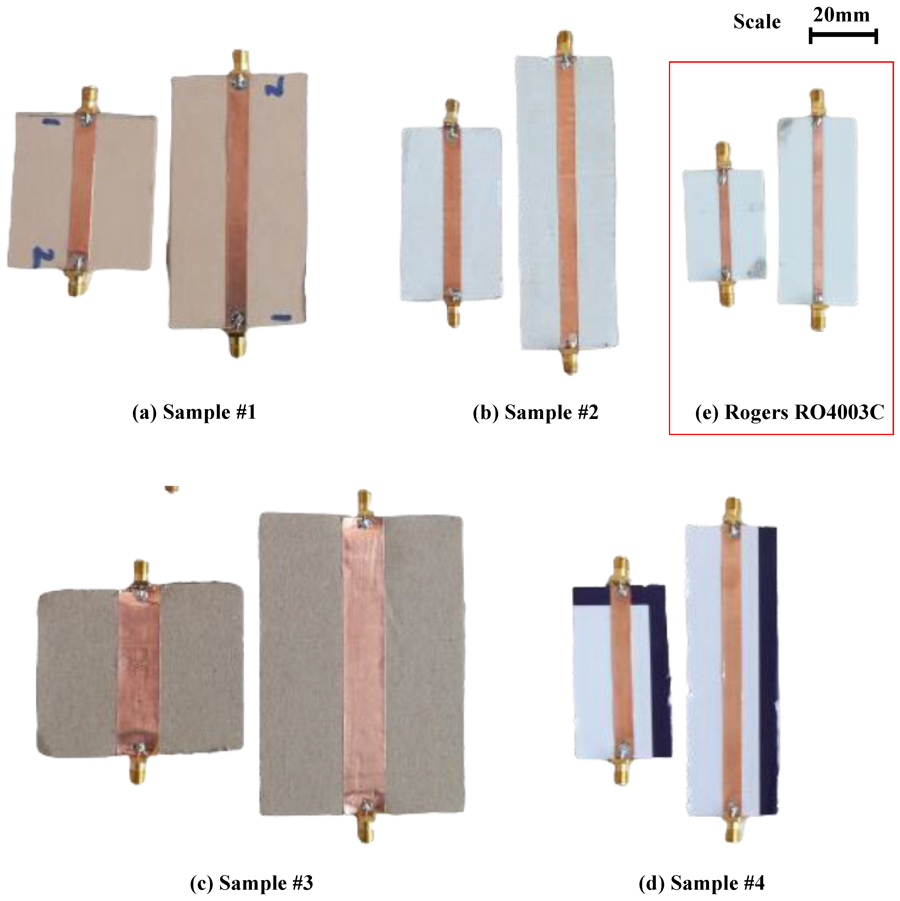
Figure 6.
Devices for the two-transmission-line method on the substrate: (a) sample #1, (b) sample #2, (c) sample #3, (d) sample #4, and (e) Rogers RO4003C as a reference sample.
Figure 6.
Devices for the two-transmission-line method on the substrate: (a) sample #1, (b) sample #2, (c) sample #3, (d) sample #4, and (e) Rogers RO4003C as a reference sample.
Figure 7.
CST simulation results: S11 variation according to the losses of the cardboard substrate.
Figure 7.
CST simulation results: S11 variation according to the losses of the cardboard substrate.
Figure 8.
CST simulation results: S11 variation according to the relative permittivity of the cardboard substrate.
Figure 8.
CST simulation results: S11 variation according to the relative permittivity of the cardboard substrate.
Figure 9.
Impact on antenna geometry of varying dielectric constant value ((a) L1 = 43.40 mm, (b) L2 = 41.70 mm, and (c) L3 = 39.5 mm are the lengths of the patch with a dielectric constant of 1.833, 1.983, and 2.2, respectively).
Figure 9.
Impact on antenna geometry of varying dielectric constant value ((a) L1 = 43.40 mm, (b) L2 = 41.70 mm, and (c) L3 = 39.5 mm are the lengths of the patch with a dielectric constant of 1.833, 1.983, and 2.2, respectively).
Figure 10.
Impact on antenna geometry of loss tangent value ((a) = 2.7 mm, (b) = 1.5 mm, and (c) = 0.8 mm are the lengths of the inset with loss tangent of 0.055, 0.063, and 0.068, respectively).
Figure 10.
Impact on antenna geometry of loss tangent value ((a) = 2.7 mm, (b) = 1.5 mm, and (c) = 0.8 mm are the lengths of the inset with loss tangent of 0.055, 0.063, and 0.068, respectively).
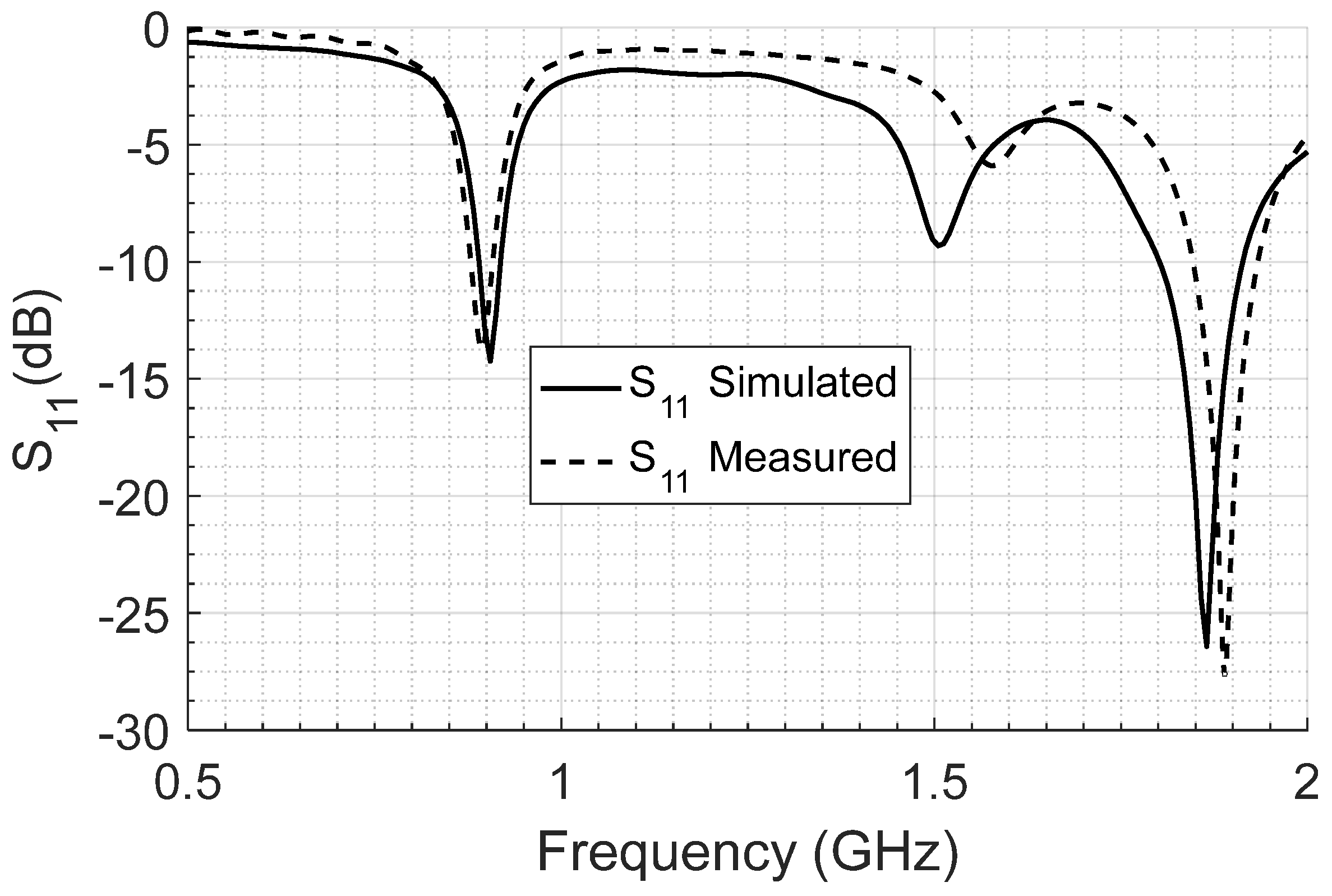
Figure 12.
Simulated and measured S
11 of the antenna on cardboard sample #4 (
Figure 11b).
Figure 12.
Simulated and measured S
11 of the antenna on cardboard sample #4 (
Figure 11b).
Figure 13.
Simulated and measured S
11 of antenna on cardboard sample #1a (
Figure 11c).
Figure 13.
Simulated and measured S
11 of antenna on cardboard sample #1a (
Figure 11c).
Figure 15.
Simulated and measured return loss of dual band patch antenna on cardboard sample #1a (smooth face).
Figure 15.
Simulated and measured return loss of dual band patch antenna on cardboard sample #1a (smooth face).
Figure 17.
Simulated and measured return loss of broadband monopole antenna on cardboard sample #1a (smooth face).
Figure 17.
Simulated and measured return loss of broadband monopole antenna on cardboard sample #1a (smooth face).
Figure 18.
Block diagram of a rectenna with an optional PMU.
Figure 18.
Block diagram of a rectenna with an optional PMU.
Figure 19.
Rectifier schematics based on the voltage-doubler topology with complete DC path.
Figure 19.
Rectifier schematics based on the voltage-doubler topology with complete DC path.
Figure 20.
Schematics of the rectifier in
Figure 19 for momentum co-simulation with configuration for cardboard sample #1 substrate.
Figure 20.
Schematics of the rectifier in
Figure 19 for momentum co-simulation with configuration for cardboard sample #1 substrate.
Figure 21.
Laboratory setup for measuring the rectified voltage of cardboard rectifier at 2.45 GHz under varying load and input power conditions: (a) schematics, (b) lab setup.
Figure 21.
Laboratory setup for measuring the rectified voltage of cardboard rectifier at 2.45 GHz under varying load and input power conditions: (a) schematics, (b) lab setup.
Figure 22.
Fabricated rectifier on cardboard sample #1a using HSMS-2860 diode according to the schematic in
Figure 20 (bottom).
Figure 22.
Fabricated rectifier on cardboard sample #1a using HSMS-2860 diode according to the schematic in
Figure 20 (bottom).
Figure 23.
Simulated and measured S11 under different input power conditions of rectifier fabricated on cardboard sample #1.
Figure 23.
Simulated and measured S11 under different input power conditions of rectifier fabricated on cardboard sample #1.
Figure 24.
Simulated and measured DC output power of cardboard sample #1 rectifier in
Figure 22 under −10 dBm input RF power at 2.45 GHz.
Figure 24.
Simulated and measured DC output power of cardboard sample #1 rectifier in
Figure 22 under −10 dBm input RF power at 2.45 GHz.
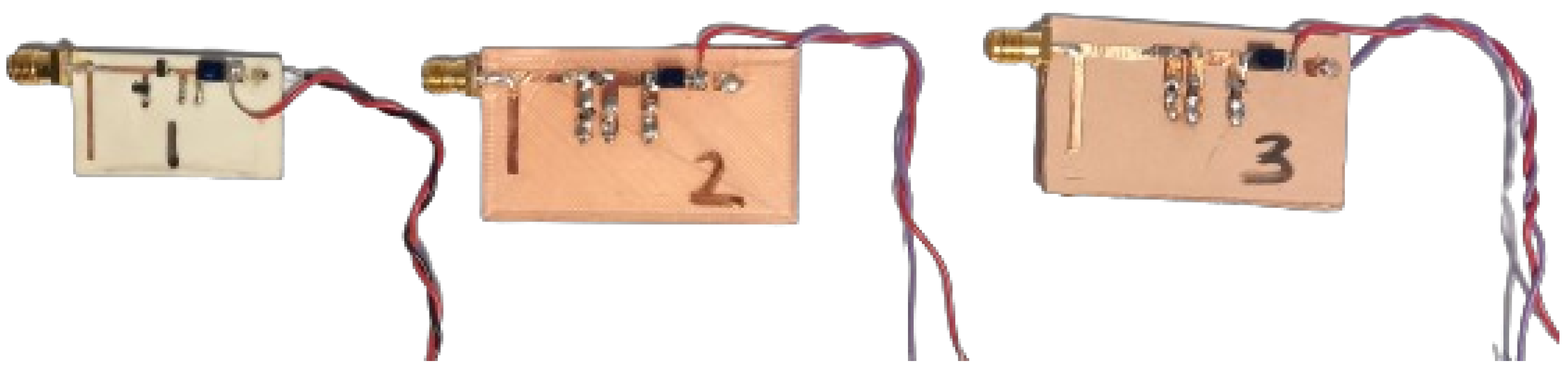
Figure 25.
Rectifiers with three different diodes on cardboard material #1a: (1) HSMS-2860, (2) HSMS-2850, (3) SMS7630-079LF 7630.
Figure 25.
Rectifiers with three different diodes on cardboard material #1a: (1) HSMS-2860, (2) HSMS-2850, (3) SMS7630-079LF 7630.
Figure 26.
Output DC power versus load for rectifiers in
Figure 25 under −10 dBm input power.
Figure 26.
Output DC power versus load for rectifiers in
Figure 25 under −10 dBm input power.
Figure 27.
Measured RF–DC output power under 0 dBm input power for rectifiers in
Figure 25.
Figure 27.
Measured RF–DC output power under 0 dBm input power for rectifiers in
Figure 25.
Figure 28.
Measured RF–DC output power under −5 dBm of input power for rectifiers in
Figure 25.
Figure 28.
Measured RF–DC output power under −5 dBm of input power for rectifiers in
Figure 25.
Figure 29.
Rectifiers on three different substrates but the same SMS7630-079LF diodes: (1) Rogers RO4003C, (2) PLA (3) cardboard #1.
Figure 29.
Rectifiers on three different substrates but the same SMS7630-079LF diodes: (1) Rogers RO4003C, (2) PLA (3) cardboard #1.
Figure 30.
Measured RF–DC power under varying load and 0 dBm of input RF power for rectifiers in
Figure 29.
Figure 30.
Measured RF–DC power under varying load and 0 dBm of input RF power for rectifiers in
Figure 29.
Figure 31.
Measured RF–DC power under varying load and −5 dBm of input RF power for rectifiers in
Figure 29.
Figure 31.
Measured RF–DC power under varying load and −5 dBm of input RF power for rectifiers in
Figure 29.
Figure 32.
Measured RF–DC power under varying load and −10 dBm of input RF power for rectifiers in
Figure 29.
Figure 32.
Measured RF–DC power under varying load and −10 dBm of input RF power for rectifiers in
Figure 29.
Table 1.
Roughness measurement of the different cardboard samples.
Table 1.
Roughness measurement of the different cardboard samples.
| Sample Name | Measurement 1 (μm) | Measurement 2 (μm) | Measurement 3 (μm) | Average (μm) |
|---|
| Sample #1 | 1.34 | 1.45 | 1.38 | 1.39 |
| Sample #1 ground | 3.14 | 3.53 | 3.85 | 3.50 |
| Copper tape on Sample #1 | 0.82 | 0.63 | 0.74 | 0.73 |
| Sample #2 | 1.79 | 1.76 | 1.67 | 1.74 |
| Sample #2 ground | 4.56 | 4.68 | 4.9 | 4.71 |
| Copper tape on Sample #2 | 0.59 | 0.61 | 0.6 | 0.6 |
| Sample #3 | 5 | 4.73 | 4.89 | 4.87 |
| Sample #3 ground | 4.8 | 5.2 | 4.9 | 4.97 |
| Sample #4 | 0.69 | 0.82 | 0.78 | 0.76 |
| Sample #4 ground | 2.7 | 3.2 | 3.27 | 3.06 |
Table 2.
Dielectric permittivity and loss tangents of cardboard paper substrates as compared with the literature.
Table 2.
Dielectric permittivity and loss tangents of cardboard paper substrates as compared with the literature.
| Frequency (GHz) | L1/L2 (mm) | Thickness (mm) | tanδ | | Method | Ref |
|---|
| 0.5–3 | 30/100 | 2.9 | 0.04–0.08 | 1.4–2.6 | Coplanar Wave-guides | [5] |
| 0.5–3 | 50/100 | 0.56 | 0.015–0.028 | 1.78–1.82 | TTL | [35] |
| 0.5–3 | 55.5/91 | 2.2 | 0.054–0.057 | 1.889–1.968 | TTL | sample #1 |
| 0.5–3 | 60/100 | 2.15 | 0.01–0.07 | 1.189–1.264 | TTL | sample #2 |
| 0.5–3 | 67/108 | 3.6 | 0.025–0.08 | 1.17–1.24 | TTL | sample #3 |
| 0.5–3 | 65/108 | 1.7 | 0.045–0.065 | 1.401–1.415 | TTL | sample #4 |
Table 3.
Simulated effect of loss tangent on antenna global gain (cardboard sample #1, dielectric constant 1.8333).
Table 3.
Simulated effect of loss tangent on antenna global gain (cardboard sample #1, dielectric constant 1.8333).
| Loss Tangent (tanδ) | Recessed Distance (mm) | S11 (dB) | Gain (dB) | Bandwidth (MHz) | Efficiency (%) |
|---|
| 0.055 | 2.7 | −43.5 | 2.46 | 146.5 | 33.9 |
| 0.063 | 1.5 | −30 | 2.03 | 154 | 31 |
| 0.068 | 0.8 | −29.85 | 1.78 | 158.2 | 29.35 |
| 0.072 | — | −26.34 | 1.58 | 160.4 | 28.14 |
Table 4.
Simulated effect of dielectric constant on antenna global gain (cardboard sample #1, loss tangent 0.055).
Table 4.
Simulated effect of dielectric constant on antenna global gain (cardboard sample #1, loss tangent 0.055).
| Dielectric Constant () | Length of Patch (mm) | S11 (dB) | Gain (dB) | Bandwidth (MHz) | Efficiency (%) |
|---|
| 1.8 | 43.40 | −33.45 | 2.46 | 147.9 | 34 |
| 1.833 | — | −28.85 | 2.54 | 146.6 | 33.7 |
| 1.933 | — | −27.25 | 2.29 | 142.8 | 33.4 |
| 1.963 | 41.70 | −26.10 | 1.88 | 142 | 33.1 |
| 2.088 | 39.5 | −24.13 | 0.319 | 138.1 | 32.8 |
Table 5.
Simulated effect of cardboard substrate thickness on antenna radiation parameters (cardboard sample #1, loss tangent 0.055).
Table 5.
Simulated effect of cardboard substrate thickness on antenna radiation parameters (cardboard sample #1, loss tangent 0.055).
| Thickness (mm) | | Lp (mm) | Wp (mm) | S11 (dB) | Gain (dB) | Bandwidth (MHz) | Efficiency (%) |
|---|
| 2.15 | 1.87 | 43.2 | 54 | −34.4 | 1.84 | 140.4 | 32.12 |
| 1.7 | 1.86 | 43.2 | 54 | −48.7 | 2.47 | 146 | 33.88 |
| 2.2 | 1.85 | 43.2 | 54 | −27.3 | 2.9 | 157.9 | 39.55 |
| 3.6 | 1.81 | 43.2 | 54 | −16.8 | 3.6 | 166.2 | 52.14 |
Table 6.
Antenna geometry (in mm) in
Figure 11.
Table 6.
Antenna geometry (in mm) in
Figure 11.
| Sample Name | Wp | Lp | Wf | Lf | Wx | Wc | Ws | Ls | H |
|---|
| Sample #1 | 54 | 41.5 | 5.4 | 21 | 21.6 | 2.7 | 88 | 80 | 1.9 |
| Sample #4 | 54 | 41.5 | 5.4 | 21 | 21.6 | 2.7 | 88 | 80 | 5.9 |
Table 7.
Main properties of patch antenna fabricated on cardboard substrates.
Table 7.
Main properties of patch antenna fabricated on cardboard substrates.
| Sample Number | Size (mm3) | Gain (dB) | Bandwidth (MHz) | Resonance Frequency (GHz) | S11 (dB) |
|---|
| #4 simulation | 80 × 88 × 1.7 | 3.12 | 136.8 | 2.4523 | −37.098 |
| #4 measurement | 80 × 88 × 1.7 | 3.01 | 109 | 2.446 | −16.204 |
| #1 simulation | 80 × 88 × 2.2 | 2.98 | 169.9 | 2.4513 | −39.76 |
| #1a measurement | 80 × 88 × 2.2 | 2.53 | 160.4 | 2.46 | −33.653 |
| #1b measurement | 80 × 88 × 2.2 | 2.51 | 168.7 | 2.45 | −25.98 |
| #1 simulation | 190 × 186 × 2.2 | 0.21 | 20 | 0.900 | −11.387 |
| #1a measurement | 190 × 186 × 2.2 | 0.45 | 25 | 0.900 | −14.15 |
| #1a simulation | 190 × 186 × 2.2 | 0.369 | 107.2 | 1.816 | −12.847 |
| #1a measurement | 190 × 186 × 2.2 | 0.54 | 120 | 1.862 | −21.15 |
Table 8.
Geometry (in mm) of antenna in
Figure 14 on cardboard sample #1a substrate.
Table 8.
Geometry (in mm) of antenna in
Figure 14 on cardboard sample #1a substrate.
| Wp | Lp | Wf | Lf | Wx1 | Wx2 | Wc | Ws | Ls | H |
|---|
| 152 | 108.1 | 7.6 | 47 | 64.2 | 63.7 | 8 | 186 | 190 | 2.2 |
Table 9.
Geometry (in mm) of the antenna in
Figure 16 on cardboard sample #1a substrate.
Table 9.
Geometry (in mm) of the antenna in
Figure 16 on cardboard sample #1a substrate.
| Lp | Ls | Lg | Ws | Wx | Lf | Sh | Sw | Sl | Wf |
|---|
| 43 | 105 | 41 | 95 | 19 | 45.1 | 4 | 16 | 6 | 5 |
Table 10.
Main properties of monopole antenna fabricated on cardboard paper substrate sample #1a (smooth face).
Table 10.
Main properties of monopole antenna fabricated on cardboard paper substrate sample #1a (smooth face).
| Sample Number | Global Gain (dB) at 2.45 GHz | Bandwidth (MHz) | S11 (dB) at 2.45 GHz | Size (mm3) |
|---|
| #1 simulation | 2.51 | 2010.2 | −16.519 | 105 × 95 × 2.2 |
| #1 measurement | 2.2 | 2132 | −22.23 | 105 × 95 × 2.2 |
Table 11.
Manufacturer characteristic parameters of most commonly used Schottky diodes in energy harvesting [
53].
Table 11.
Manufacturer characteristic parameters of most commonly used Schottky diodes in energy harvesting [
53].
| Diode | Vth (V) | Rs (Ω) | Cjo (pF) | Is (μA) | BV (V) |
|---|
| MA4E1317 | 0.70 | 4 | 0.02 | 0.1 | 7.0 |
| HSMS 2852 | 0.15 | 25 | 0.18 | 3.0 | 3.8 |
| HSMS 2850 | 0.15 | 25 | 0.18 | 3.0 | 3.8 |
| HSMS 2860 | 0.25 | 6.0 | 0.18 | 0.05 | 7.0 |
| HSMS 286B | 0.69 | 6 | 0.18 | 0.05 | 7.0 |
| HSMS 2820 | 0.15 | 6 | 0.70 | 0.022 | 15.0 |
| SMS 7630-079LF | 0.09 | 20 | 0.14 | 5.0 | 2.0 |
Table 12.
Optimal output load values in kΩ for rectifiers with HSMS-2850, HSMS-2860, and SMS7630-079LF diodes under different input power levels.
Table 12.
Optimal output load values in kΩ for rectifiers with HSMS-2850, HSMS-2860, and SMS7630-079LF diodes under different input power levels.
| Power (dBm) | SMS7630-079LF | HSMS-2850 | HSMS-2860 |
|---|
| 0 | 1.1 | 1 | 2 |
| −5 | 1.5 | 1.5 | 3 |
| −10 | 2 | 2.6 | 8 |
Table 13.
Comparison of rectifier output performances.
Table 13.
Comparison of rectifier output performances.
| Freq. (GHz) | Pin (dBm)@Load (kΩ) | PCE@RF–DC Power (μW) | Substrate/Print Tech | Size (mm3) | Ref |
|---|
| 2.45 | 0 @ 5 | 39.2%@392 | Rogers RT/Duroid 5880/PCB | 60 × 40 × 1.57 | [21] |
| 2.45 | 0 @ 7 | 50%@500 | LCP/not mentioned | 15.1 × 8.15 × 0.18 | [25] |
| 2.3 | −24 @ 14.7 | 5%@0.2 | FR4/printed circuit board | 70 × 70 × 13.2 | [9] |
| 2.45 | −20 @ 20 | 6%@0.6 | Rogers RT (Duroid) 5880/printed circuit board | 60 × 40 × 1.57 | [21] |
| 2.45 | −15@1.7 | 19%@ 6 | PLA/fuse deposition modeling 3D printing polymer | 42 × 14 × 1.5 | [7] |
| | −20 @ 2 | 24%@0.96 | | | |
| | −25 @ 3.9 | 5%@0.14 | | | |
| 2.45 | 0 @ 2.4 | 41.5%@ 415 | Rogers RO4003C/PCB | 35 × 17 × 1.5 | This work |
| | −5@3 | 36.4%@115 | | | |
| | −10 @ 3.5 | 27.5%@27.5 | | | |
| 2.45 | 0 @1.1 | 22%@ 220 | Cardboard #1/copper tape | 50 × 20 × 2.2 | This work |
| | −5 @ 1.5 | 14.2%@45 | | | |
| | −10@2 | 8.5%@8.5 | | | |


 ,
, 


