Abstract
This paper presents a design for timing mismatch calibration in a TIADC (Time-Interleaved Analog-to-Digital Converter) with wideband inputs. By exploiting the approximately linear relationship between the autocorrelation properties of sub-ADCs and timing mismatch, we achieve rapid convergence of error estimation. A low-cost detection method is proposed based on the convergent monotonicity of the Least Mean Square (LMS) algorithm, which can automatically correct the calibration direction when the input signal goes beyond the Nyquist zone. Physical test results indicate that the spurs caused by timing mismatch can be suppressed by 26–30 dB using the proposed method.
1. Introduction
As the world enters the era of 5G (5th generation) communications and big data, the demand for information is exploding. Ultra-high-speed ADCs are widely used in modern communication systems, such as WiFi, software-defined radio, and electronic measuring instruments. A single ADC is constrained by factors such as its own structure and process, which make it unable to simultaneously meet the performance requirements of high precision, a high conversion rate, and low power consumption. In an ideal situation, the Time-Interleaved Analog-to-Digital Converter (TIADC) greatly improves the sampling rate of the system by simultaneously sampling multiple sub-channel ADCs [1,2,3,4].
However, under real-world conditions, the linearity of the TIADC system output will deteriorate significantly due to errors such as offset mismatch, gain mismatch, and timing mismatch between the channels. High-energy spurs will be generated in the output spectrum, which can reduce the SFDR and SNR and also affect the effective number of bits of the output [5]. Compared with other mismatches, timing mismatch will drastically deteriorate the performance of the TIADC system as the frequency of the input signal increases [6]. Therefore, the calibration of timing mismatches plays a vital role in the entire TIADC system. Existing calibration methods for timing mismatch errors can be divided into calibration with a reference signal and calibration with its own signal, depending on whether it includes an additional reference channel [7,8,9,10]. We can naturally divide the calibration into two steps: detection and correction. From the correction structure, it can be divided into the analog domain [11,12,13,14] and the digital domain [15,16,17]. Analog calibration typically involves utilizing a tunable delay line in the sampling clock [5,18]. The key distinction lies in the resistance [11] or capacitance [18] of the delay circuit.
Timing mismatch can be easily estimated through digital methods. These methods assume that the slope of the signal is first-order equivalent and utilize the product of the timing mismatch and the signal derivative (time deviation) in the digital domain to eliminate the error caused by the timing mismatch. The time deviation detection method can be roughly divided into two categories: one based on deterministic equalization detection [14,19] and the other based on statistical information of the input signal [10].
The time deviation detection method based on deterministic equalization, in the context of time-skew detection, is a direct and effective approach to correct the various non-ideal factors of the ADC by utilizing an additional converter for equalization as a reference [20,21]. However, referencing the ADC will lead to an increased power consumption and area. The reference converter also periodically changes the TIADC’s input impedance, resulting in additional spurious signals that depend on the signal. A digital differentiator implemented by an FIR filter can accurately calculate the slope of the input signal [22,23]. However, this method has inherent constraints and may fail to operate effectively when the input signal approaches or exceeds the Nyquist frequency. By increasing the number of taps in the FIR filter, the digital differentiator can operate over a wider Nyquist frequency range [24]. However, this method poses significant challenges regarding the digital hardware area and power consumption [25,26]. In addition to the digital differential, there is another method to obtain the slope of the signal. By using two ADCs to sample the same input but with different bandwidths, it is possible to determine the difference between the two ADCs [18]. By adding a resistor to the sampling network of the other ADC to make its sampling bandwidth different from that of the reference ADC, the disparity between the two ADCs enables the estimation of the signal slope. This method can only determine the slope of the signal when the reference ADC samples, but it cannot determine the slope at all positions. Therefore, this method is only suitable for use with analog tuning correction.
However, the digital calibration compensation method often requires a higher hardware cost to achieve a better compensation accuracy as the frequency of the input signal increases [27]. Using multipliers operating at high clock frequencies will result in a significant power consumption penalty. Most of the aforementioned methods impose restrictions on the frequency of the input signal, which cannot exceed the Nyquist zone [11,14,17]. This limitation hampers the TIADC system in undersampling scenarios.
In this paper, a wideband timing mismatch calibration design for a TIADC with fast convergence is proposed. We accelerate the convergence process of timing mismatch estimation by tracking the sign information of the sub-ADC’s autocorrelation properties. A low-cost direction correction module based on convergence monotonicity is introduced into the TIADC system to address the issue of incorrect calibration direction when the input signal exceeds the Nyquist zone.
2. The Proposed Calibration Design
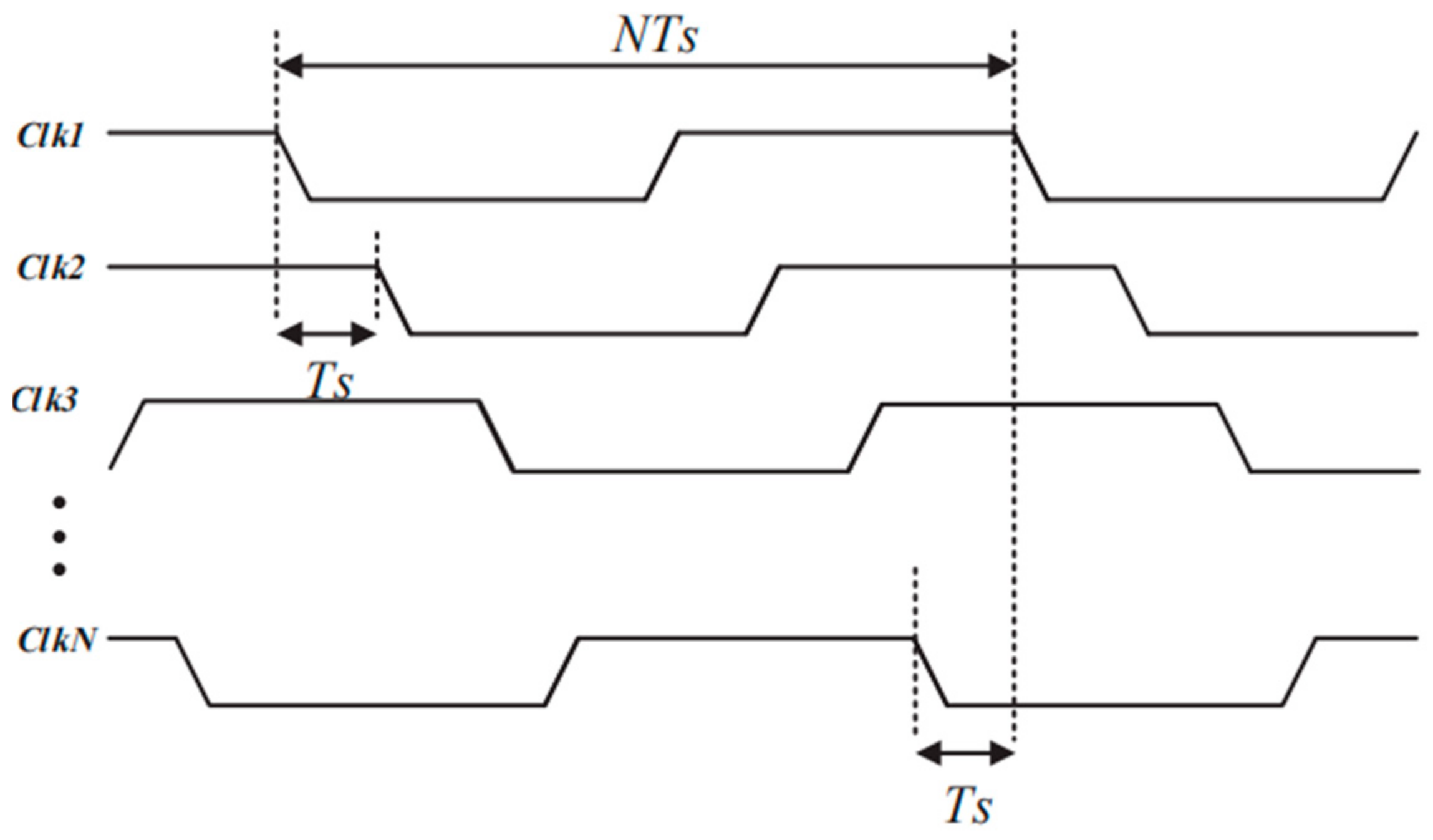
We assume that the offset and gain mismatches have already been corrected and only focus on the timing mismatch. The detailed system block diagram is shown in Figure 1, where Sub-ADC1, Sub-ADC2, ..., Sub-ADCN represent N sub-channel ADCs of the TIADC system [5]. These sub-channel ADCs are driven by the output of the clock generator, as illustrated in Figure 2. The variable delay line is composed of a switched capacitor array, with their status being switched by the error estimate Dcalib generated by the error estimation module. The convergence direction monitor module is introduced to detect and correct the convergence direction.
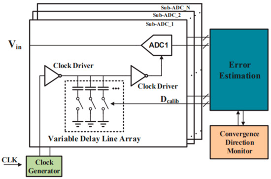
Figure 1.
TIADC system block diagram.
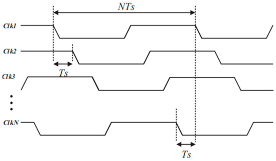
Figure 2.
N divided clock.
2.1. Timing Mismatch Estimation and Compensation
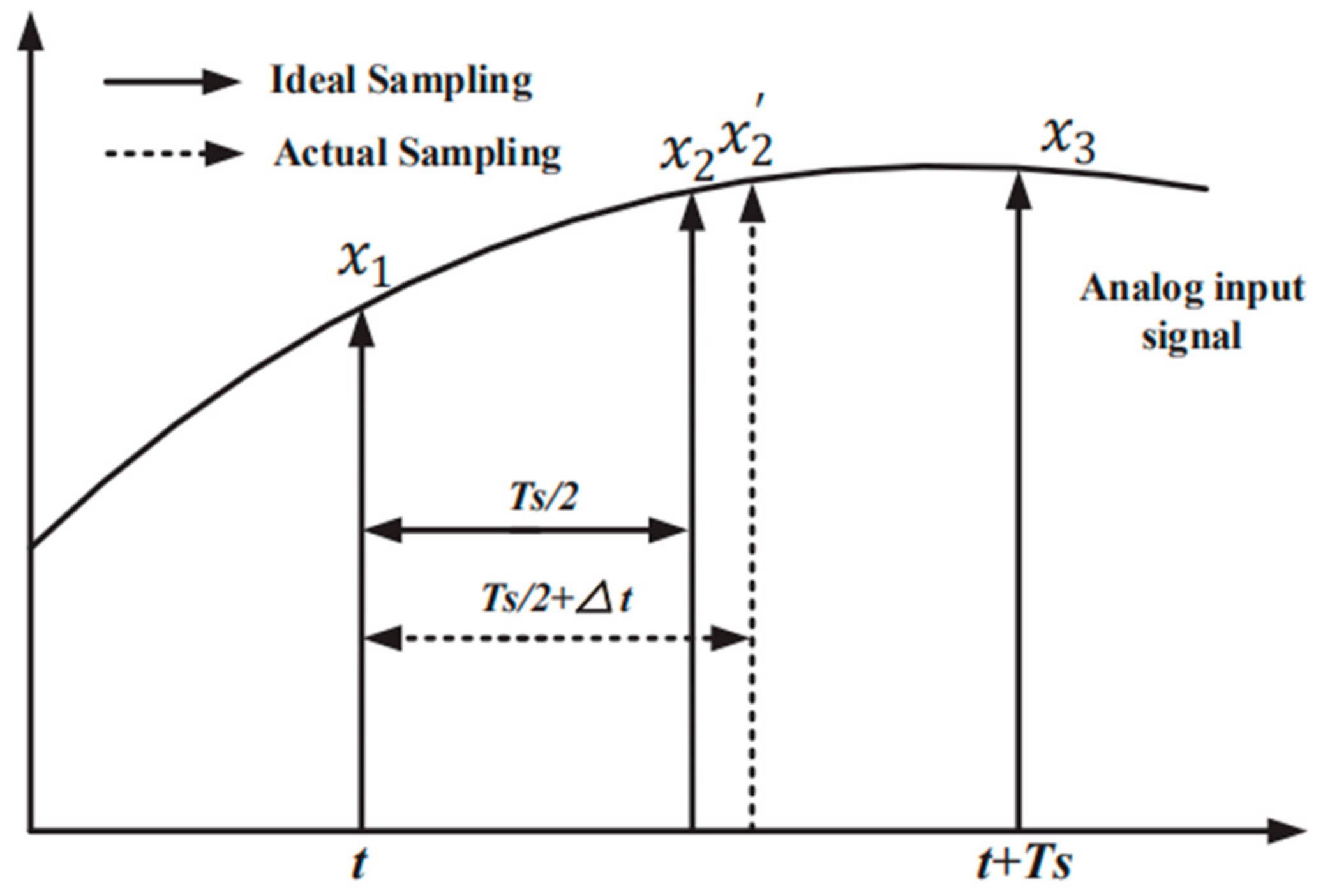
We take a traditional two-channel TIADC as an example. The timing mismatch is shown in Figure 3.
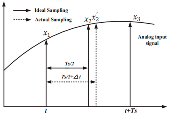
Figure 3.
Timing mismatch.
Take the CH1 as the reference channel. Let x1 be the sampled value of CH1 at time t, x2 be the sampled value of CH2 at the ideal sampling time t + Ts/2, x′2 be the sampled value of CH2 at the sampling time t + Ts/2 + ∆t with timing mismatch ∆t, and x3 be the sampled value of CH1 at time t + Ts. In the case of ∆t ≪ Ts, the error value between CH1 and CH2 can be presented as follows [11]:
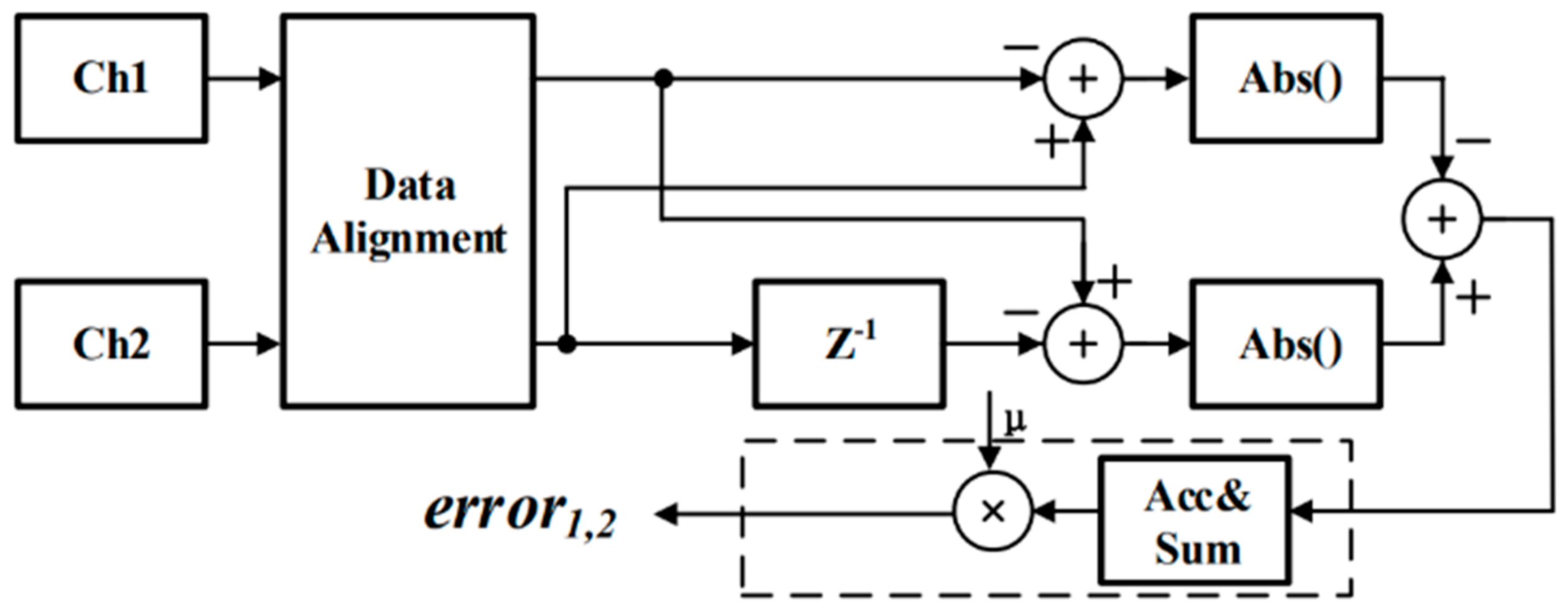
where E represents expectation and R represents the cross-correlation function of Ts. To simplify the calculation and reduce the hardware costs, the expectation is replaced by the cumulative average, and the square operation is replaced by the absolute value. Based on the LMS algorithm [20,22], error1,2 can be estimated as follows,
where µ indicates the step size, as we know, which is a trade-off between the convergence speed and accuracy. The block diagram of the timing mismatch estimation is shown in Figure 4.
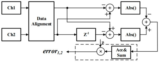
Figure 4.
Timing mismatch estimation design.
After obtaining the estimated value of the error between channels, the error value is mapped to a control code word. The correction feedback loop adjusts the switched capacitor array in sub-ADCs based on the control code word mentioned above. This can help adjust the sampling clock delay for each channel, minimizing timing discrepancies between channels.
The traditional estimation method can achieve stable convergence when µ is small enough. However, this is often accompanied by the issue of a slow convergence speed. Additionally, when the input signal goes beyond the Nyquist zone, the traditional estimation method will fail due to an incorrect calibration direction.
2.2. Mismatch Estimation Fast Convergence
The linear relationship in (1) indicates that the error1,2 will change sign in an overcompensated condition. In our method, we perform a window averaging operation on the iteration quantity and obtain its sign information.
Let
We can rewrite (2) as
Then, the convergence process can be divided into three parts: 1. the fast approach part; 2. the reverse correction part; and 3. the oscillation convergence part. In the fast approach part, we choose a constant large step value to rapidly reach the overcompensated condition. When the sign of α is inverted, we select a small step value that corresponds to 1 LSB of the delay line control codeword, and then proceed to the reverse correction part. This process will continue until the sign of α inverse changes again, indicating that we have neared the final convergence value. At this point, the iterative formula will be replaced by (2) to achieve the oscillation convergence phase.
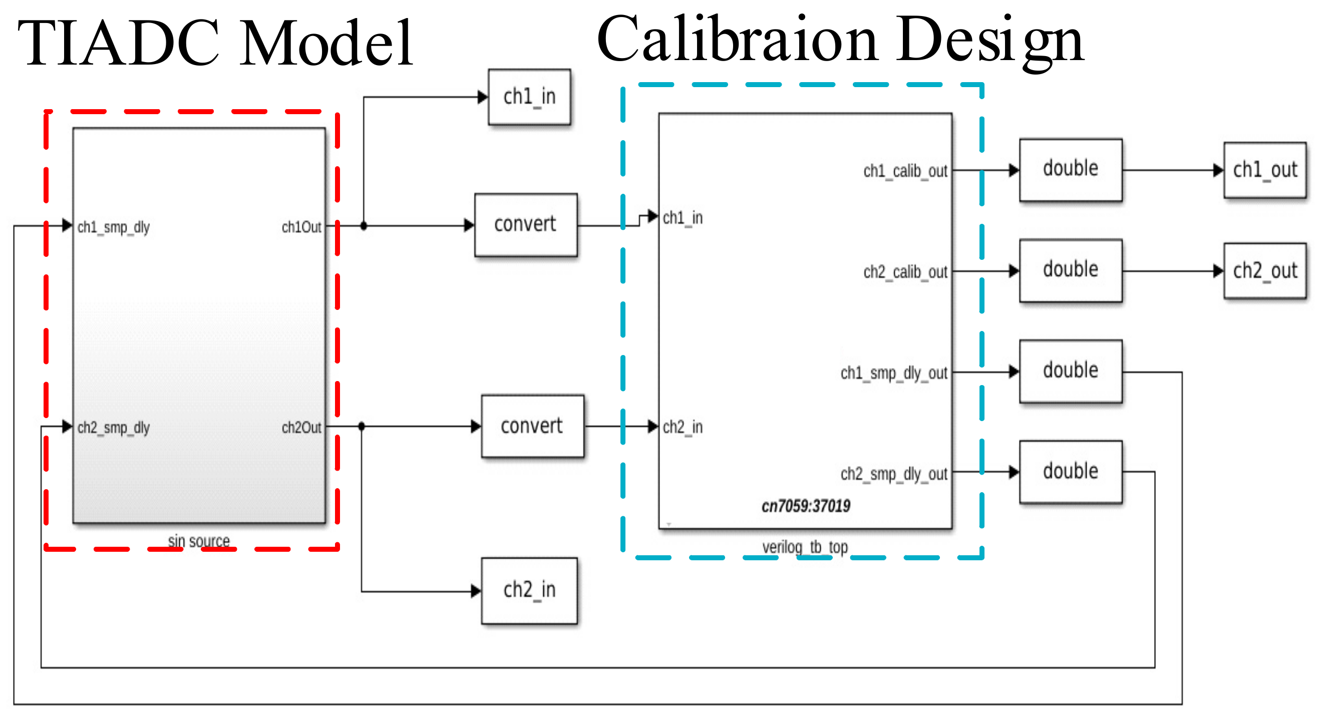
We constructed a two-channel 14-bit TIADC model with timing mismatch, operating at 2 GS/s in Simulink v9.2. The delay compensation utilizes a variable delay line array with an accuracy of 1 ps and is mapped to an 8-bit control codeword. The calibration algorithm implemented in Verilog HDL code performs behavioral co-simulation. The entire simulation platform is illustrated in Figure 5. On the left, within the red dashed box, is the SIMULINK mathematical model of the two-channel time-interleaved ADC and ideal delay line. On the right, within the blue dashed box, is the Verilog HDL code design for timing mismatch calibration. This section also includes a data-type conversion module for converting between floating-point and fixed-point numbers.
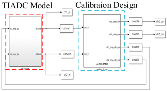
Figure 5.
Simulation platform.
The input frequency signal is normalized to a frequency of fs1 = 0.11fs, respectively. The inter-channel timing mismatch is set to ∆t/Ts = 0.0026. Figure 6 shows the convergence speed comparison between the proposed method and the traditional method, where µ is set to 2−7. It can be seen from Figure 7 that the convergence accuracy of the two methods is within ±2 LSB delay line control codeword precision. The spectra of the TIADC output are shown in Figure 8. The simulation results show that the proposed method drastically reduces the convergence time and effectively inhibits timing mismatch spurs.
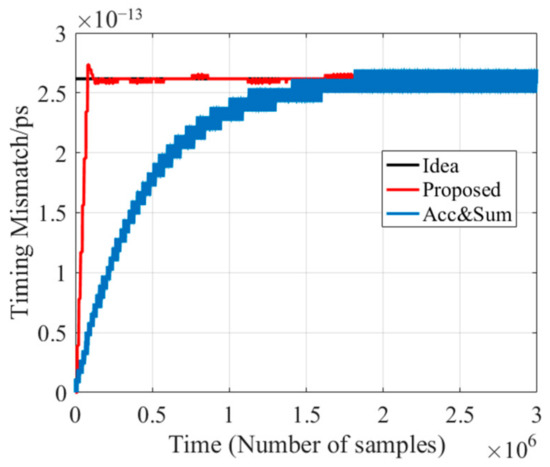
Figure 6.
Convergence speed comparison.
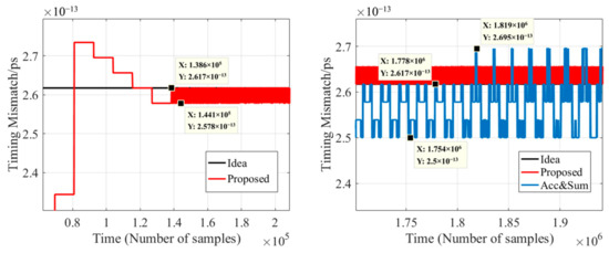
Figure 7.
Comparison of convergence accuracy.
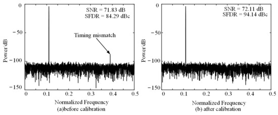
Figure 8.
First Nyquist zone input signal calibration simulation result.
2.3. Calibration Direction Auto Correction
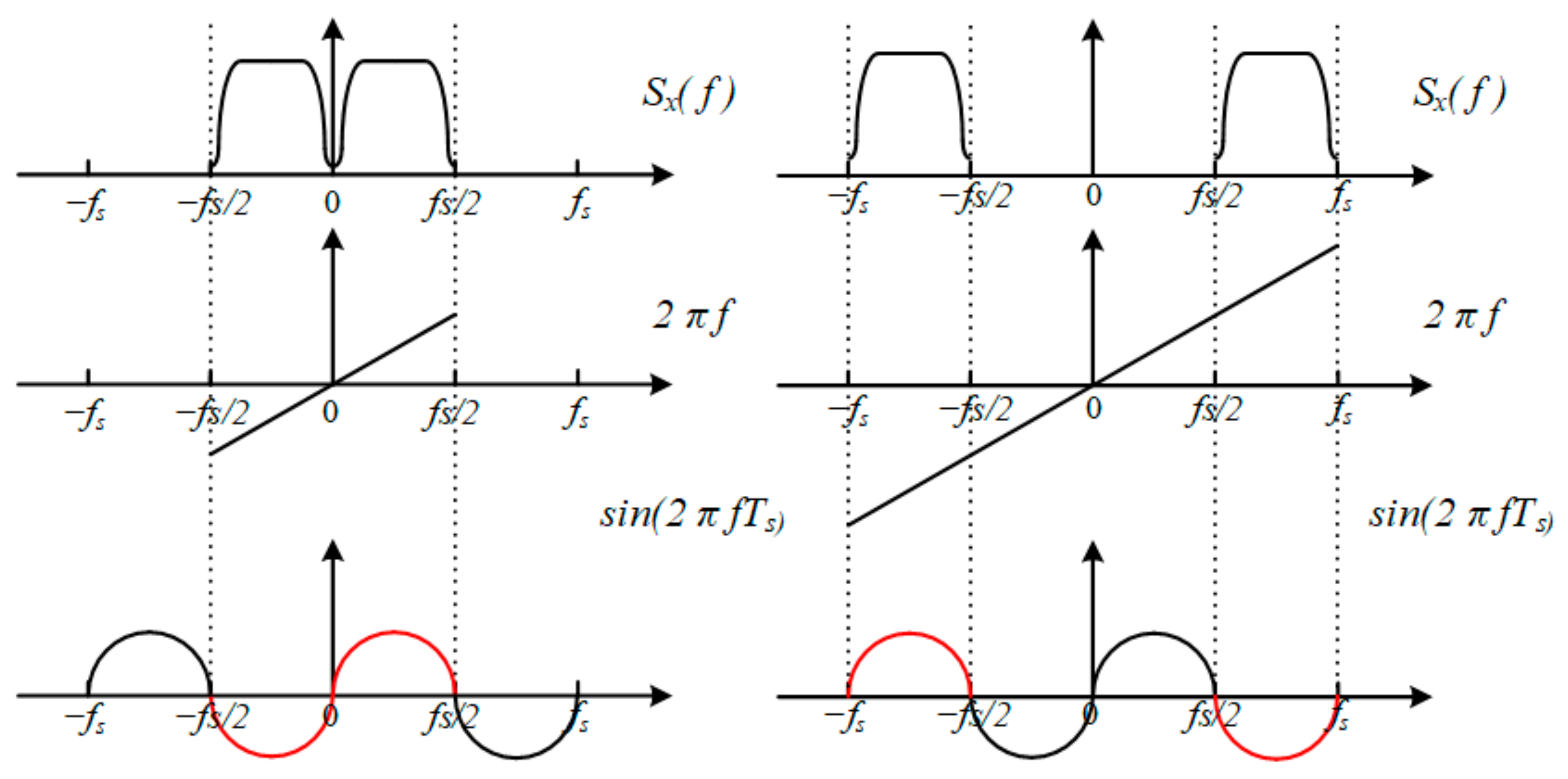
It can be shown from [28] that the derivative of the autocorrelation is given by
where Sx(f) represents a real input signal spectrum and exhibits an even symmetry. We can recognize from Figure 9 that when the signal spectrum is located in different Nyquist zones, the sign of Equation (5) exhibits a reverse periodicity due to the sine function.
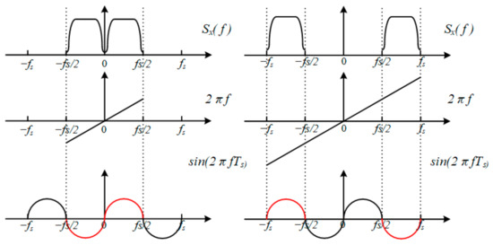
Figure 9.
Multiplication of spectra.
The simulation results of input signals at different frequencies from the first to the second Nyquist zone are shown in Figure 10.
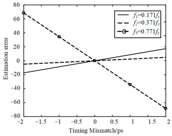
Figure 10.
Convergence direction corresponding to different frequency intervals.
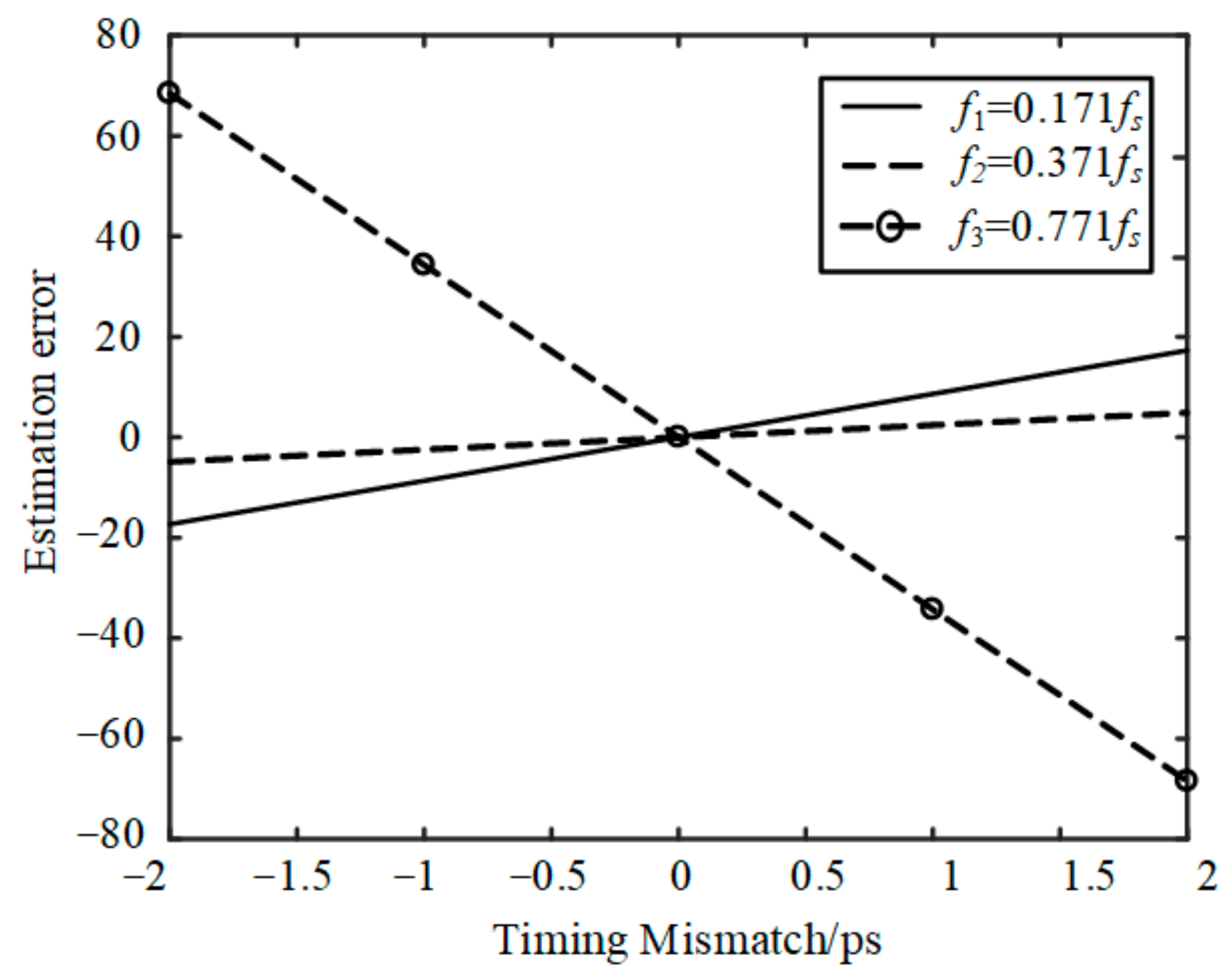
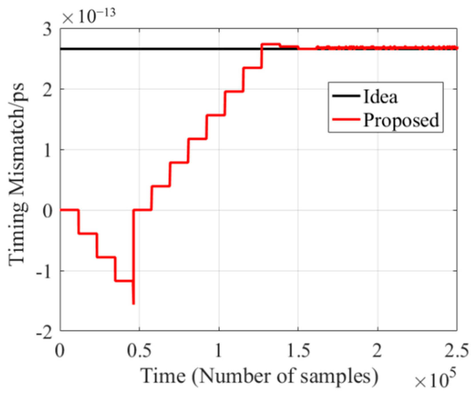
The opposite sign will lead to the wrong convergence direction, which can cause the calibration to fail. According to the LMS principle [11,20,22], we know that when the convergence is in the right direction, α will gradually decrease and eventually converge to the oscillation’s final value. When the signs are opposite, the incorrect convergence direction will cause error1,2 to increase further. At the same time, due to the approximately linear relationship between α and error1,2, α will also increase. Based on this rule, we introduce a simple method to correct the convergence direction. At the beginning of the calibration, we use a two-window period to monitor the monotonic variation in error1,2. If error1,2 continuously and monotonically increases, this indicates that the current calibration direction is incorrect. In this case, we abandon all the steps taken and reverse the calibration direction. Following the simulation conditions in Section 2.1 and changing the input frequency to fs2 = 0.66fs, the entire process of convergence direction calibration is illustrated in Figure 11. It can be seen from Figure 11 that the estimation error is reset to 0 after the direction of convergence briefly goes in the wrong direction. Then, the estimation error converges in the correct direction and eventually stabilizes around the ideal error value. The spectra of the TIADC output are shown in Figure 12, and the timing mismatch is effectively suppressed.

Figure 11.
Convergence direction correction.
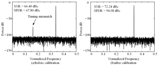
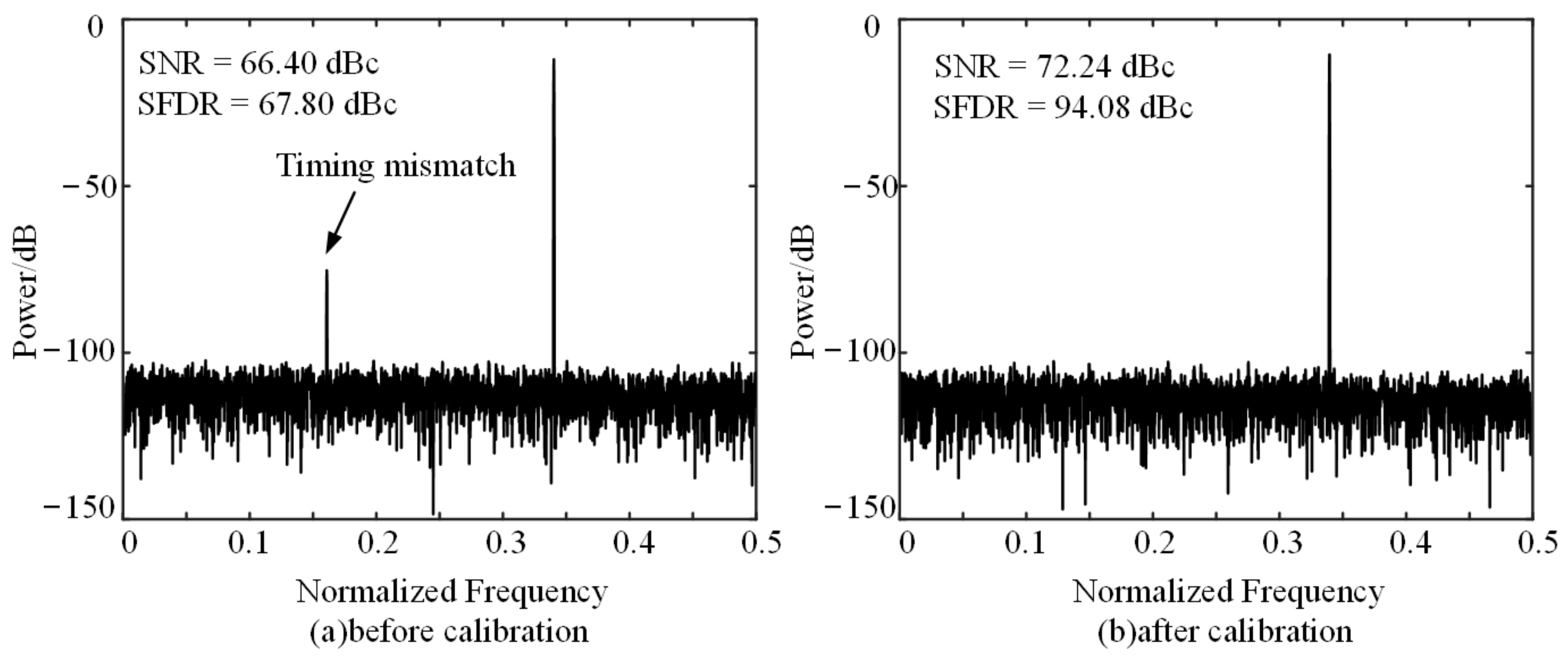
Figure 12.
Second Nyquist zone input signal calibration simulation result.
The input signal covers the entire first and second Nyquist zones for verification, as shown in Figure 13. The results show that the proposed calibration method in this paper is still applicable for wideband inputs, and the spurious-free dynamic range (SFDR) is significantly improved compared to the case without calibration.
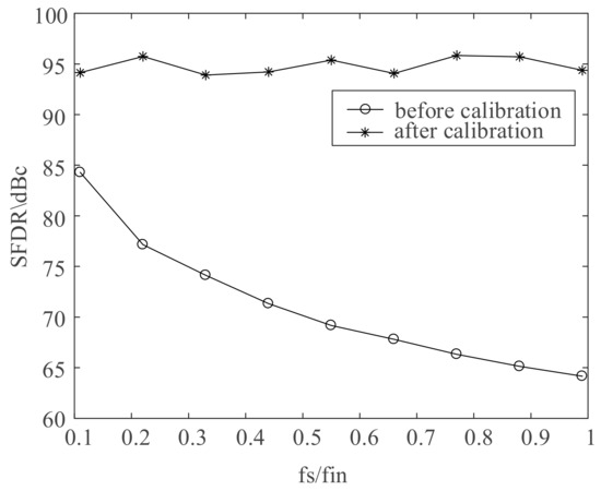
Figure 13.
SFDR comparison before and after calibration covering the first and second Nyquist zones.
3. Physical Test Results
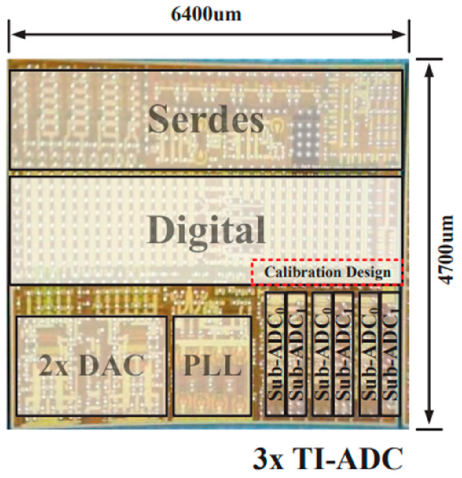
The two-channel 14-bit 2.56-GS/s TIADC, including the timing mismatch correction and compensation circuits, was fabricated using 28 nm digital CMOS technology. The die photograph of the 2T/3R RF transceiver chip, which incorporates three TIADCs and was primarily intended for small base stations, is depicted in Figure 14, with the design section highlighted by a red dotted box.
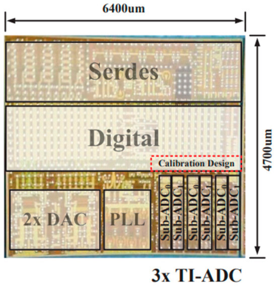
Figure 14.
Die photograph.
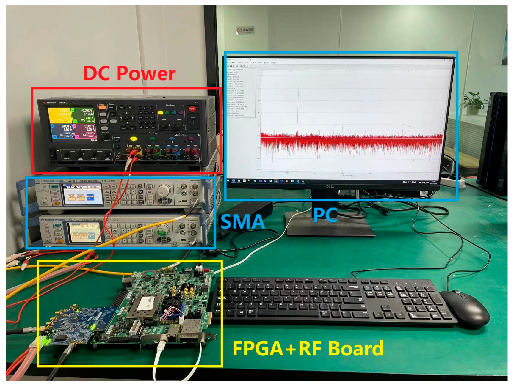
The setup of the entire physical test bench is shown in Figure 15. It includes a PC running MATLAB 2018b software for processing sampled data, an FPGA board connected to an RF board for data acquisition, a DC power supply for system operation, and two SMA connectors used for providing a reference clock and input signals, respectively.

Figure 15.
Physical test bench.
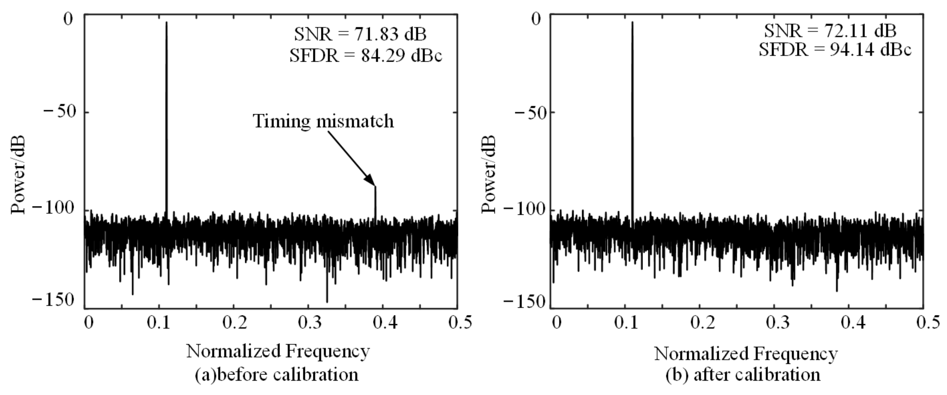
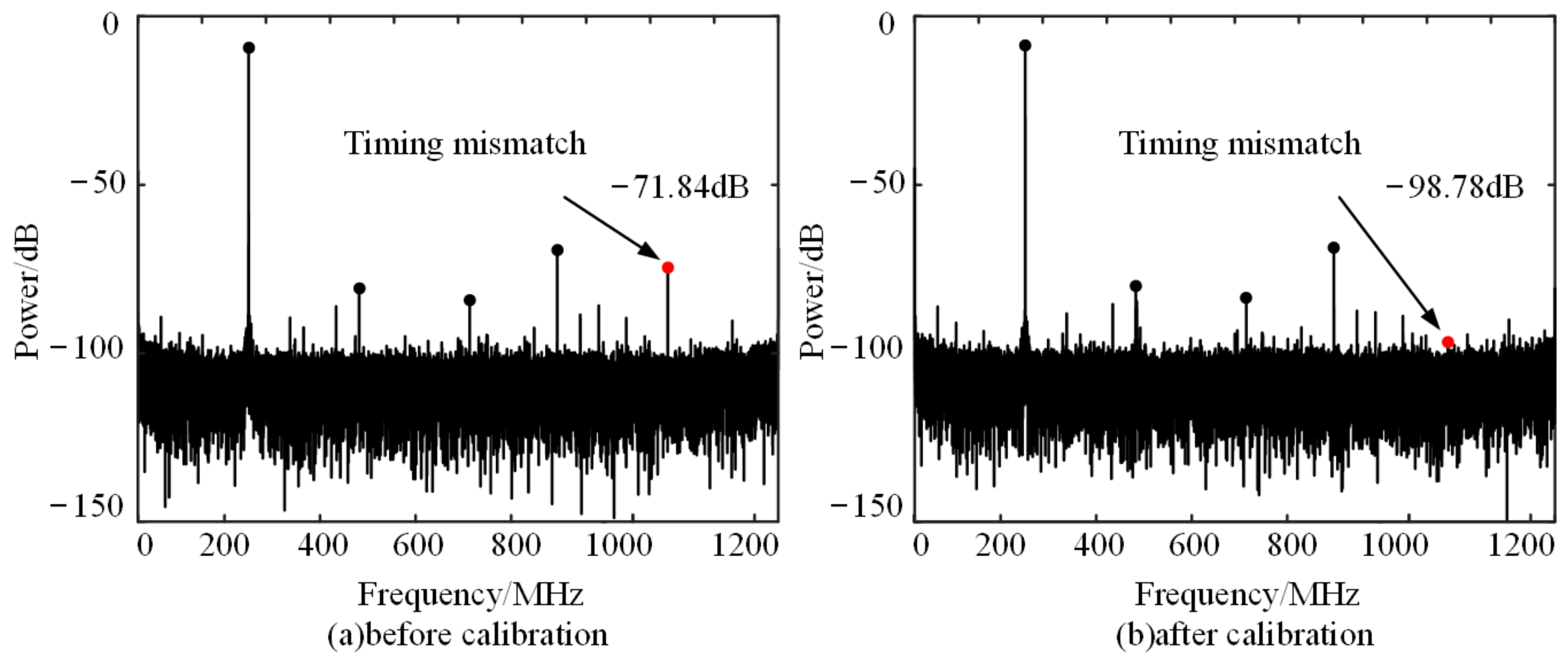
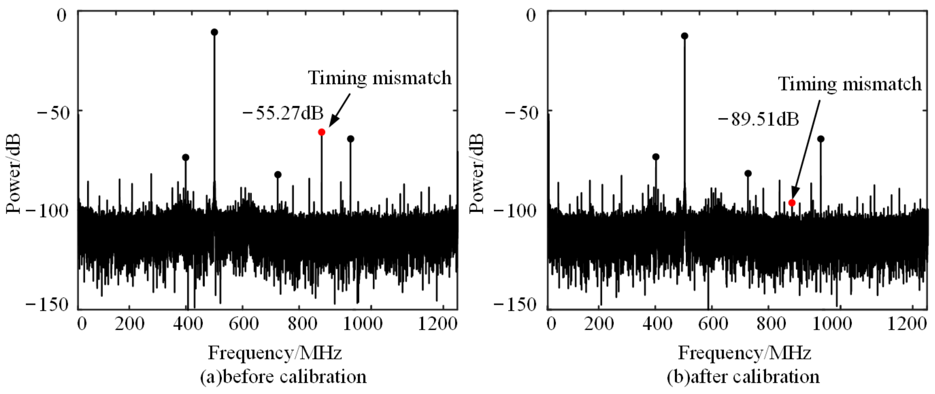
Figure 16 and Figure 17 display the measured output spectra with 0.221 GHz and 2.101 GHz inputs before and after calibration.

Figure 16.
First Nyquist zone input signal measurement result.

Figure 17.
Second Nyquist zone input signal measurement result.
The measurement results show that the proposed method can achieve excellent calibration results. The spurs caused by the timing mismatch are significantly reduced when the input signal is in the first or second Nyquist zones.
The design features compared to those in reference papers are listed in Table 1. The proposed method in this paper achieves excellent mismatch spur suppression while converging faster. And thanks to the automatic direction correction design, the input signal of the proposed method can exceed the Nyquist zone.

Table 1.
Comparison with references.
4. Conclusions
In this paper, we have proposed a low-complexity calibration design for TIADC timing mismatch. By utilizing the sign information of the sub-ADC’s autocorrelation properties, the convergence process is accelerated compared to traditional methods. Furthermore, a low-cost automatic direction correction design is proposed to ensure the accuracy of the calibration algorithm even when the input signal exceeds the Nyquist zone. The effectiveness of the proposed method in this paper is demonstrated through simulation and physical testing, and the spurious effects caused by timing mismatch can be suppressed by 26–30 dB. However, the calibration design proposed in this paper also has some limitations and shortcomings. Due to its reliance on the autocorrelation statistical characteristics of the input signal, it requires the input signal frequency to be coprime with the TIADC sampling frequency. Additionally, the selection of large step-size iteration constants during the initial fast approach part and the iteration parameter µ during the final oscillation convergence part needs careful consideration based on practical circumstances to achieve the best calibration results.
Author Contributions
Investigation, G.H. and D.X.; methodology, G.H. and D.X.; validation, G.H. and P.G.; writing—original draft preparation, G.H., D.X. and P.G.; writing—review and editing, M.Z. and G.H.; supervision, M.Z., J.L. and Z.W. All authors have read and agreed to the published version of the manuscript.
Funding
This research received no external funding.
Data Availability Statement
Data are contained within the article.
Conflicts of Interest
Author Peng Gao was employed by the company China United Network Communications Co., Ltd. The remaining authors declare that the research was conducted in the absence of any commercial or financial relationships that could be construed as a potential conflict of interest.
References
- Chen, C.-Y.; Wu, J.; Hung, J.-J.; Li, T.; Liu, W.; Shih, W.-T. A 12-Bit 3 GS/s Pipeline ADC With 0.4 mm2 and 500 mW in 40 nm Digital CMOS. IEEE J. Solid-State Circuits 2012, 47, 1013–1021. [Google Scholar] [CrossRef]
- Janssen, E.; Doris, K.; Zanikopoulos, A.; Murroni, A.; van der Weide, G.; Lin, Y.; Alvado, L.; Darthenay, F.; Fregeais, Y. An 11b 3.6GS/s time-interleaved SAR ADC in 65 nm CMOS. In Proceedings of the 2013 IEEE International Solid-State Circuits Conference Digest of Technical Papers, San Francisco, CA, USA, 17–21 February 2013; pp. 464–465. [Google Scholar]
- Doris, K.; Janssen, E.; Nani, C.; Zanikopoulos, A.; van der Weide, G. A 480 mW 2.6 GS/s 10b Time-Interleaved ADC With 48.5 dB SNDR up to Nyquist in 65 nm CMOS. IEEE J. Solid-State Circuits 2011, 46, 2821–2833. [Google Scholar] [CrossRef]
- Guo, M.; Sin, S.-W.; Qi, L.; Xu, D.; Wang, G.; Martins, R.P. Background Timing Mismatch Calibration Techniques in High-Speed Time-Interleaved ADCs: A Tutorial Review. IEEE Trans. Circuits Syst. II Express Briefs 2022, 69, 2564–2569. [Google Scholar] [CrossRef]
- Razavi, B. Design Considerations for Interleaved ADCs. IEEE J. Solid-State Circuits 2013, 48, 1806–1817. [Google Scholar] [CrossRef]
- Wang, C.-Y.; Wu, J.-T. A background timing-skew calibration technique for time-interleaved analog-to-digital converters. IEEE Trans. Circuits Syst. II Express Briefs 2006, 53, 299–303. [Google Scholar] [CrossRef]
- Kang, H.-W.; Hong, H.-K.; Kim, W.; Ryu, S.-T. A Time-Interleaved 12-b 270-MS/s SAR ADC With Virtual-Timing-Reference Timing-Skew Calibration Scheme. IEEE J. Solid-State Circuits 2018, 53, 2584–2594. [Google Scholar] [CrossRef]
- Liu, W.; Chiu, Y. Time-Interleaved Analog-to-Digital Conversion with Online Adaptive Equalization. IEEE Trans. Circuits Syst. I Regul. Pap. 2012, 59, 1384–1395. [Google Scholar] [CrossRef]
- Ni, M.; Wang, X.; Li, F.; Rhee, W.; Wang, Z. A 13-Bit 2-GS/s Time-Interleaved ADC with Improved Correlation-Based Timing Skew Calibration Strategy. IEEE Trans. Circuits Syst. I Regul. Pap. 2022, 69, 481–494. [Google Scholar] [CrossRef]
- El-Chammas, M.; Murmann, B. A 12-GS/s 81-mW 5-bit Time-Interleaved Flash ADC with Background Timing Skew Calibration. IEEE J. Solid-State Circuits 2011, 46, 838–847. [Google Scholar] [CrossRef]
- Wei, H.; Zhang, P.; Datta Sahoo, B.; Razavi, B. An 8-Bit 4-GS/s 120-mW CMOS ADC. In Proceedings of the IEEE 2013 Custom Integrated Circuits Conference, San Jose, CA, USA, 22–25 September 2013; pp. 1–4. [Google Scholar]
- Lee, S.; Chandrakasan, A.P.; Lee, H.-S. A 1 GS/s 10b 18.9 mW Time-Interleaved SAR ADC With Background Timing Skew Calibration. IEEE J. Solid-State Circuits 2014, 49, 2846–2856. [Google Scholar] [CrossRef]
- Song, J.; Ragab, K.; Tang, X.; Sun, N. A 10-b 800-MS/s Time-Interleaved SAR ADC With Fast Variance-Based Timing-Skew Calibration. IEEE J. Solid-state Circuits 2017, 52, 2563–2575. [Google Scholar] [CrossRef]
- Kang, H.-W.; Hong, H.-K.; Park, S.; Kim, K.-J.; Ahn, K.-H.; Ryu, S.-T. A Sign-Equality-Based Background Timing-Mismatch Calibration Algorithm for Time-Interleaved ADCs. IEEE Trans. Circuits Syst. II Express Briefs 2016, 63, 518–522. [Google Scholar] [CrossRef]
- Yin, Y.; Sun, K.; Chen, H.; Wang, X.; Liu, L.; Deng, H.; Meng, X.; Li, K.; Wang, Z. Calibration of timing mismatch in tiadc based on monotonicity detecting of sampled data. IEICE Electron. Express 2020, 17, 20190699. [Google Scholar] [CrossRef]
- Li, D.; Zhu, Z.; Ding, R.; Liu, M.; Yang, Y.; Sun, N. A 10-Bit 600-MS/s Time-Interleaved SAR ADC With Interpolation-Based Timing Skew Calibration. IEEE Trans. Circuits Syst. II Express Briefs 2018, 66, 16–20. [Google Scholar] [CrossRef]
- Li, D.; Ding, R.; Zhu, Z.; Yang, Y. A Background Timing Skew Calibration Technique in Time-Interleaved ADCs With Second Order Compensation. In Proceedings of the 2018 IEEE Asia Pacific Conference on Circuits and Systems (APCCAS), Chengdu, China, 26–30 October 2018; pp. 53–56. [Google Scholar]
- Stepanovic, D.; Nikolic, B. A 2.8 GS/s 44.6 mW Time-Interleaved ADC Achieving 50.9 dB SNDR and 3 dB Effective Resolution Bandwidth of 1.5 GHz in 65 nm CMOS. IEEE J. Solid-state Circuits 2013, 48, 971–982. [Google Scholar] [CrossRef]
- Chang, D.-J.; Choi, M.; Ryu, S.-T. A 28-nm 10-b 2.2-GS/s 18.2-mW Relative-Prime Time-Interleaved Sub-Ranging SAR ADC With On-Chip Background Skew Calibration. IEEE J. Solid-State Circuits 2021, 56, 2691–2700. [Google Scholar] [CrossRef]
- Chiu, Y.; Tsang, C.W.; Nikolic, B.; Gray, P.R. Least mean square adaptive digital background calibration of pipelined analog-to-digital converters. IEEE Trans. Circuits Syst. I Regul. Pap. 2004, 51, 38–46. [Google Scholar] [CrossRef]
- Chiu, Y. Equalization techniques for nonlinear analog circuits. IEEE Commun. Mag. 2011, 49, 132–139. [Google Scholar] [CrossRef]
- Oshima, T.; Takahashi, T.; Yamawaki, T. LMS calibration of sampling timing for time-interleaved A/D converters. Electron. Lett. 2009, 45, 615–617. [Google Scholar] [CrossRef]
- Guo, M.; Mao, J.; Sin, S.-W.; Wei, H.; Martins, R.P. A 10b 1.6GS/s 12.2mW 7/8-way Split Time-interleaved SAR ADC with Digital Background Mismatch Calibration. In Proceedings of the 2019 IEEE Custom Integrated Circuits Conference (CICC), Austin, TX, USA, 14–17 April 2019; pp. 1–4. [Google Scholar]
- Le Dortz, N.; Blanc, J.P.; Simon, T.; Verhaeren, S.; Rouat, E.; Urard, P.; Le Tual, S.; Goguet, D.; Lelandais-Perrault, C.; Benabes, P. 22.5 A 1.62GS/s time-interleaved SAR ADC with digital background mismatch calibration achieving interleaving spurs below 70dBFS. In Proceedings of the 2014 IEEE International Solid-State Circuits Conference Digest of Technical Papers (ISSCC), San Francisco, CA, USA, 9–13 February 2014; pp. 386–388. [Google Scholar]
- Le Duc, H.; Nguyen, D.M.; Jabbour, C.; Desgreys, P.; Jamin, O.; Nguyen, V.T. Fully Digital Feedforward Background Calibration of Clock Skews for Sub-Sampling TIADCs Using the Polyphase Decomposition. IEEE Trans. Circuits Syst. I Regul. Pap. 2017, 64, 1515–1528. [Google Scholar] [CrossRef]
- Guo, M.; Mao, J.; Sin, S.-W.; Wei, H.; Martins, R.P. A 5 GS/s 29 mW Interleaved SAR ADC With 48.5 dB SNDR Using Digital-Mixing Background Timing-Skew Calibration for Direct Sampling Applications. IEEE Access 2020, 8, 138944–138954. [Google Scholar] [CrossRef]
- Devarajan, S.; Singer, L.; Kelly, D.; Pan, T.; Silva, J.; Brunsilius, J.; Rey-Losada, D.; Murden, F.; Speir, C.; Bray, J.; et al. A 12-b 10-GS/s Interleaved Pipeline ADC in 28-nm CMOS Technology. IEEE J. Solid-State Circuits 2017, 52, 3204–3218. [Google Scholar] [CrossRef]
- Bendat, J.S.; Piersol, A.G. Random Data: Analysis and Measurement Procedures; John Wiley & Sons: Hoboken, NJ, USA, 2011. [Google Scholar]
- Niu, H.; Yuan, J. A Spectral-Correlation-Based Blind Calibration Method for Time-Interleaved ADCs. IEEE Trans. Circuits Syst. I Regul. Pap. 2020, 67, 5007–5017. [Google Scholar] [CrossRef]


Disclaimer/Publisher’s Note: The statements, opinions and data contained in all publications are solely those of the individual author(s) and contributor(s) and not of MDPI and/or the editor(s). MDPI and/or the editor(s) disclaim responsibility for any injury to people or property resulting from any ideas, methods, instructions or products referred to in the content. |
© 2024 by the authors. Licensee MDPI, Basel, Switzerland. This article is an open access article distributed under the terms and conditions of the Creative Commons Attribution (CC BY) license (https://creativecommons.org/licenses/by/4.0/).