


Switching-on Delay Jitter Caused by Lateral Distribution of Current Channel of Avalanche Transistor

Abstract
:1. Introduction
2. Theoretical Analysis
2.1. Principle Analysis of Switching-on Delay Jitter
2.2. Base Transit Time in One-Dimensional Case
2.3. Base Transit Time in Two-Dimensional Case
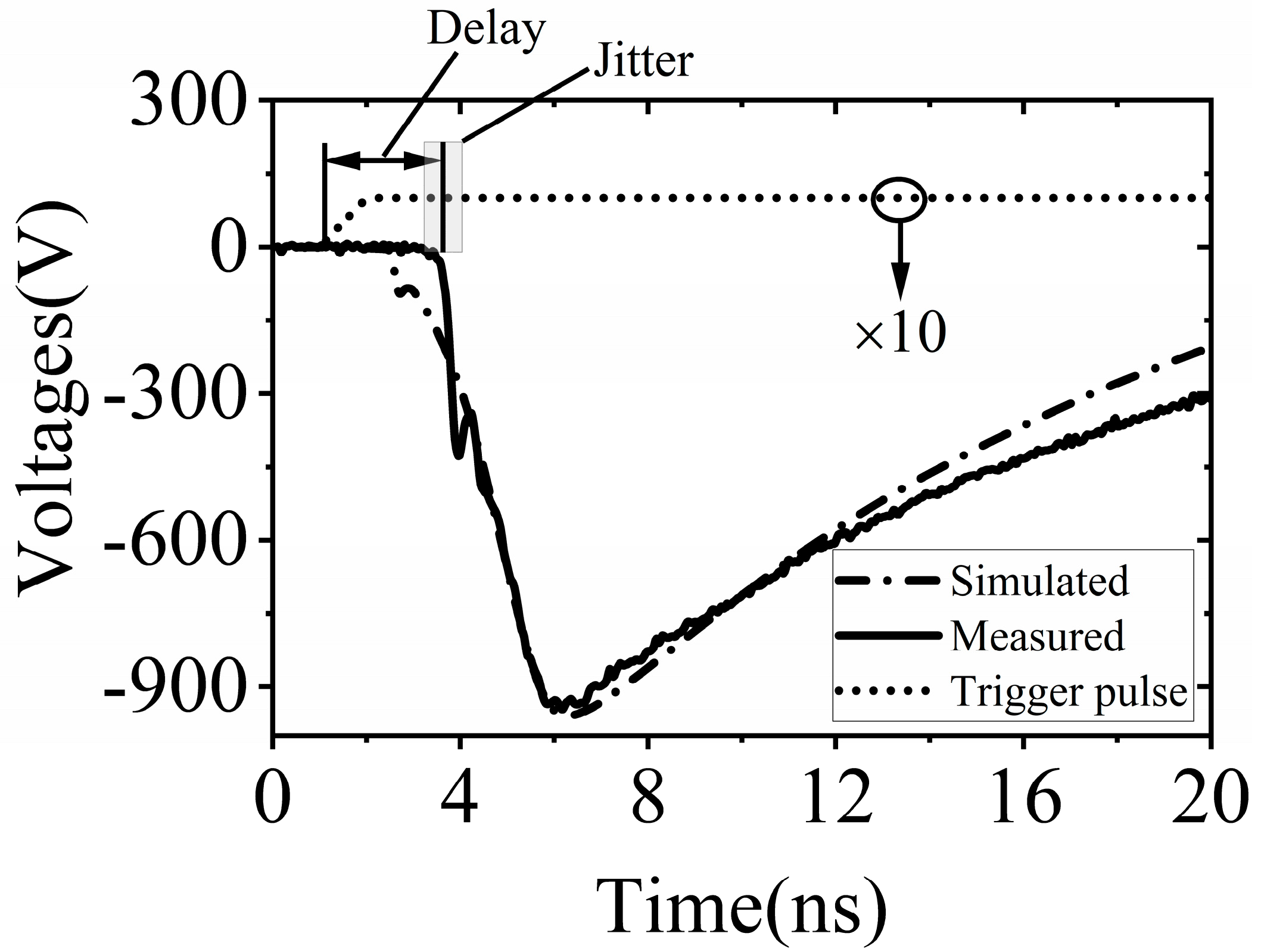
3. Simulation and Experiment
4. Discussion
4.1. Trigger Signal Changes Switching-on Delay Jitter
4.2. Potential Distribution Makes Lateral Distribution of Electron Current
5. Conclusions
Supplementary Materials
Author Contributions
Funding
Data Availability Statement
Conflicts of Interest
References
- Peng, P.; Song, H.; Zhang, T.; Addy, M.; Zhang, Y.; Cheng, Y.; Hatzenbeller, R.; Zhu, X.; Liu, S.; Liu, Y.; et al. Concentrated High Intensity Electric Field (CHIEF) System for Non-Thermal Pasteurization of Liquid Foods: Modeling and Simulation of Fluid Mechanics, Electric Analysis, and Heat Transfer. Comput. Chem. Eng. 2017, 97, 183–193. [Google Scholar] [CrossRef]
- Kavitha, S.; Raja Prabhu, R.; Raghavan, K.; Sinthu, M.; Mansoor Usman, S.; Sriram Kumar, M.; Madan Kumar, V.; Vignesh, S.; Malini, V.; Cherian, K.M.; et al. Effective Electro-Chemo-Therapy for Proliferation Control of Adult Human Mesenchymal Stem Cells. J. Electrost. 2011, 69, 267–274. [Google Scholar] [CrossRef]
- Pi, S.; Yu, Q.; Wang, T.; Lin, J. A Marx-Based Gaussian Monocycle Pulse Generator with Low Ringing Level for Ground Penetrating Radar Applications. IEEE Trans. Power Electron. 2023, 38, 9907–9916. [Google Scholar] [CrossRef]
- Liu, H.; Yao, C.; Zhao, Y.; Chen, X.; Dong, S.; Wang, L.; Davalos, R.V. In Vitro Experimental and Numerical Studies on the Preferential Ablation of Chemo-Resistant Tumor Cells Induced by High-Voltage Nanosecond Pulsed Electric Fields. IEEE Trans. Biomed. Eng. 2021, 68, 2400–2411. [Google Scholar] [CrossRef] [PubMed]
- Ramezani, M.; Shayegani Akmal, A.A.; Niayesh, K. Solid-State High-Voltage Pulse Generator for Low Temperature Plasma Ion Mobility Spectrometry. IEEE Trans. Plasma Sci. 2019, 47, 1629–1636. [Google Scholar] [CrossRef]
- Karimov, A.; Feghhi, R.; Sabzevari, F.M.; Winter, R.S.C.; Fedosejevs, R.; Rambabu, K. Design and Development of a High-Power Pulse Transmitter for Underground Environmental Perception. IEEE Trans. Microw. Theory Tech. 2022, 70, 2891–2903. [Google Scholar] [CrossRef]
- Shen, S.; Yan, J.; Wang, Y.; Sun, G.; Ding, W. Further Investigations on a Modified Avalanche Transistor-Based Marx Bank Circuit. IEEE Trans. Instrum. Meas. 2020, 69, 8506–8513. [Google Scholar] [CrossRef]
- Huang, J.S.T. Study of Transistor Switching Circuit Stability in the Avalanche Region. IEEE J. Solid-State Circuits 1967, 2, 10–21. [Google Scholar] [CrossRef]
- Cheng, Z.; Ning, H.; Tang, C.; Yan, Y.; Zhao, W.; Zhu, M.; Cai, H. Influence of Avalanche Transistor Switching Mode on Waveform Characteristics of Solid-State Pulse Source. Rev. Sci. Instrum. 2023, 94, 104708. [Google Scholar] [CrossRef] [PubMed]
- Duan, G.; Vainshtein, S.; Kostamovaara, J. Turn-on Spread Determines the Size of the Switching Region in an Avalanche Transistor. Appl. Phys. Lett. 2012, 100, 193505. [Google Scholar] [CrossRef]
- Vainshtein, S.N.; Duan, G.; Filimonov, A.V.; Kostamovaara, J.T. Switching Mechanisms Triggered by a Collector Voltage Ramp in Avalanche Transistors with Short-Connected Base and Emitter. IEEE Trans. Electron Devices 2016, 63, 3044–3048. [Google Scholar] [CrossRef]
- Xu, H.; Liu, B.; Gou, Y.; Tian, J.; Yang, Y.; Feng, P.; Wang, X.; Wei, S. Research on Triode Based High Re-Frequency Ultrafast Electrical Pulse Generation Technology. Electronics 2023, 12, 1950. [Google Scholar] [CrossRef]
- Deng, Z.; Yuan, Q.; Ding, W.; Wang, Y.; Ren, L.; Wan, Z. Self-Triggering Topology for High-Power Nanosecond Pulse Generators Based on Avalanche Transistors Marx Bank Circuits and Linear Transformer Driver. Rev. Sci. Instrum. 2022, 93, 054702. [Google Scholar] [CrossRef] [PubMed]
- Gao, M.; Xie, Y.; Wang, S.; Qiu, Y.; Li, K.; Wang, S.; Lai, Y. A Portable Ultrawideband Electromagnetic Radiator with a 1.4 MW/50 kHz Solid-State Subnanosecond Pulser. Rev. Sci. Instrum. 2019, 90, 066102. [Google Scholar] [CrossRef] [PubMed]
- Vainshtein, S.N.; Kostamovaara, J.T.; Myllyla, R.A.; Kilpela, A.J.; Maatta, K.E.A. Automatic Switching Synchronisation of Serial and Parallel Avalanche Transistor Connections. Electron. Lett. 1996, 32, 950–952. [Google Scholar] [CrossRef]
- Vainshtein, S.N.; Yuferev, V.S.; Kostamovaara, J.T. Properties of the Transient of Avalanche Transistor Switching at Extreme Current Densities. IEEE Trans. Electron Devices 2002, 49, 142–149. [Google Scholar] [CrossRef]
- Duan, G.; Vainshtein, S.N.; Kostamovaara, J.T. Modified High-Power Nanosecond Marx Generator Prevents Destructive Current Filamentation. IEEE Trans. Power Electron. 2017, 32, 7845–7850. [Google Scholar] [CrossRef]
- Vainshtein, S.; Yuferev, V.; Kostamovaara, J. Nondestructive Current Localization upon High-Current Nanosecond Switching of an Avalanche Transistor. IEEE Trans. Electron Devices 2003, 50, 1988–1990. [Google Scholar] [CrossRef]
- Qiu, Y.; Xie, Y.; Gao, M.; Wang, S.; Li, K.; Wang, S.; Gu, Y.-H.; Lai, Y. High Power and High Pulse Repetition Frequency Transistorized Pulser by Time Base Stability Improvement and Power Synthesis Technique. Rev. Sci. Instrum. 2020, 91, 084703. [Google Scholar] [CrossRef] [PubMed]
- Li, J.; Zhong, X.; Li, J.; Liang, Z.; Chen, W.; Li, Z.; Li, T. Theoretical Analysis and Experimental Study on an Avalanche Transistor-Based Marx Generator. IEEE Trans. Plasma Sci. 2015, 43, 3399–3405. [Google Scholar] [CrossRef]
- Pierret, R.F. Semiconductor Device Fundamentals; Addison Wesley: Boston, MA, USA, 1996; pp. 414–419. [Google Scholar]
- Singh, J. Semiconductor Devices: Basic Principles; John Wiley & Sons: Hoboken, NJ, USA, 2000; pp. 201–206. [Google Scholar]
- Suzuki, K.; Nakayama, N. Base Transit Time of Shallow-Base Bipolar Transistors Considering Velocity Saturation at Base-Collector Junction. IEEE Trans. Electron Devices 1992, 39, 623–628. [Google Scholar] [CrossRef]
- Hassan, M.M.S.; Nomani, M.W.K. Base-Transit-Time Model Considering Field Dependent Mobility for BJTs Operating at High-Level Injection. IEEE Trans. Electron Devices 2006, 53, 2532–2539. [Google Scholar] [CrossRef]
- Van Overstraeten, R.J.; DeMan, H.J.; Mertens, R.P. Transport Equations in Heavy Doped Silicon. IEEE Trans. Electron Devices 1973, 20, 290–298. [Google Scholar] [CrossRef]
- Chowdhury, M.I.B.; Hassan, M.M.S. Analysis of Base Transit Time for a Bipolar Junction Transistor Considering Base Current. In Proceedings of the International Conference on Electrical & Computer Engineering (ICECE 2010), Dhaka, Bangladesh, 18–20 December 2010; pp. 20–24. [Google Scholar]
- Selberherr, S. Analysis and Simulation of Semiconductor Devices; Springer: Vienna, Austria, 2012; pp. 103–117. [Google Scholar]


| Trigger Signal | Llateral | Switching-on Delay Jitter |
|---|---|---|
| #1 | 2.1 μm | 30~71 ps |
| #2 | 2.4 μm | 39~92 ps |
| #3 | 2.7 μm | 49~117 ps |
Disclaimer/Publisher’s Note: The statements, opinions and data contained in all publications are solely those of the individual author(s) and contributor(s) and not of MDPI and/or the editor(s). MDPI and/or the editor(s) disclaim responsibility for any injury to people or property resulting from any ideas, methods, instructions or products referred to in the content. |
© 2024 by the authors. Licensee MDPI, Basel, Switzerland. This article is an open access article distributed under the terms and conditions of the Creative Commons Attribution (CC BY) license (https://creativecommons.org/licenses/by/4.0/).
Share and Cite
Cheng, Z.; Ning, H.; Tang, C.; Yan, Y.; Zhao, W. Switching-on Delay Jitter Caused by Lateral Distribution of Current Channel of Avalanche Transistor. Electronics 2024, 13, 2451. https://doi.org/10.3390/electronics13132451
Cheng Z, Ning H, Tang C, Yan Y, Zhao W. Switching-on Delay Jitter Caused by Lateral Distribution of Current Channel of Avalanche Transistor. Electronics. 2024; 13(13):2451. https://doi.org/10.3390/electronics13132451
Chicago/Turabian StyleCheng, Zhenbo, Hui Ning, Chuanxiang Tang, Youjie Yan, and Wei Zhao. 2024. "Switching-on Delay Jitter Caused by Lateral Distribution of Current Channel of Avalanche Transistor" Electronics 13, no. 13: 2451. https://doi.org/10.3390/electronics13132451
APA StyleCheng, Z., Ning, H., Tang, C., Yan, Y., & Zhao, W. (2024). Switching-on Delay Jitter Caused by Lateral Distribution of Current Channel of Avalanche Transistor. Electronics, 13(13), 2451. https://doi.org/10.3390/electronics13132451