

Three-Dimensional Lattice Structure to Reduce Parasitic Inductance for WBG Power Semiconductor-Based Converters


Abstract
:1. Introduction
2. Proposed Parasitic Inductance Reduction Structure with Three-Dimensional Magnetic Flux Cancellation
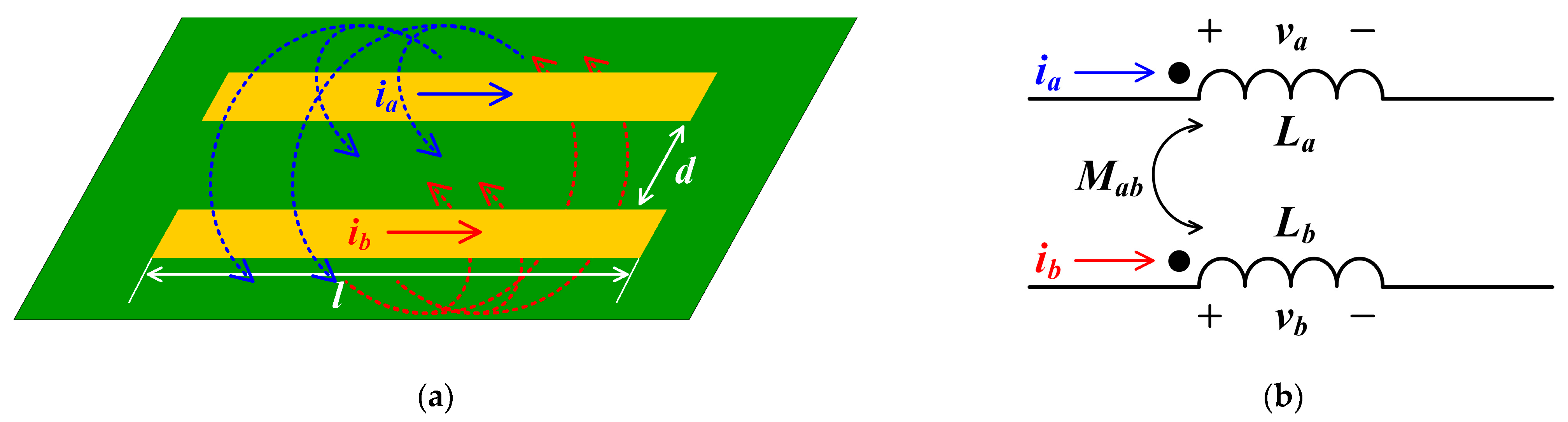
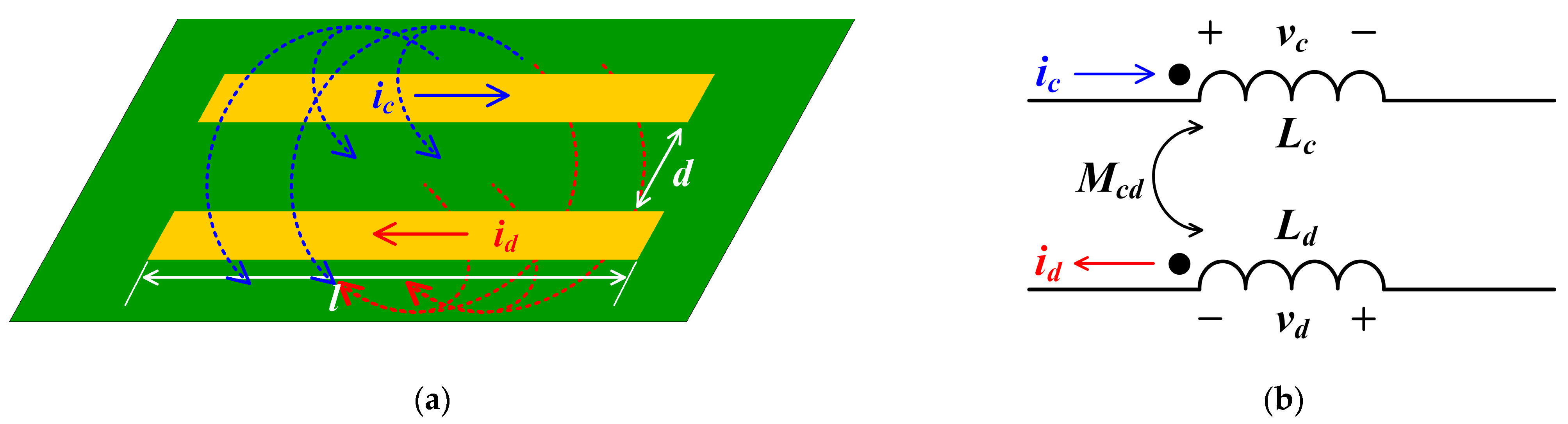
2.1. Relationship between Parasitic Inductance and Magnetic Flux Cancellation
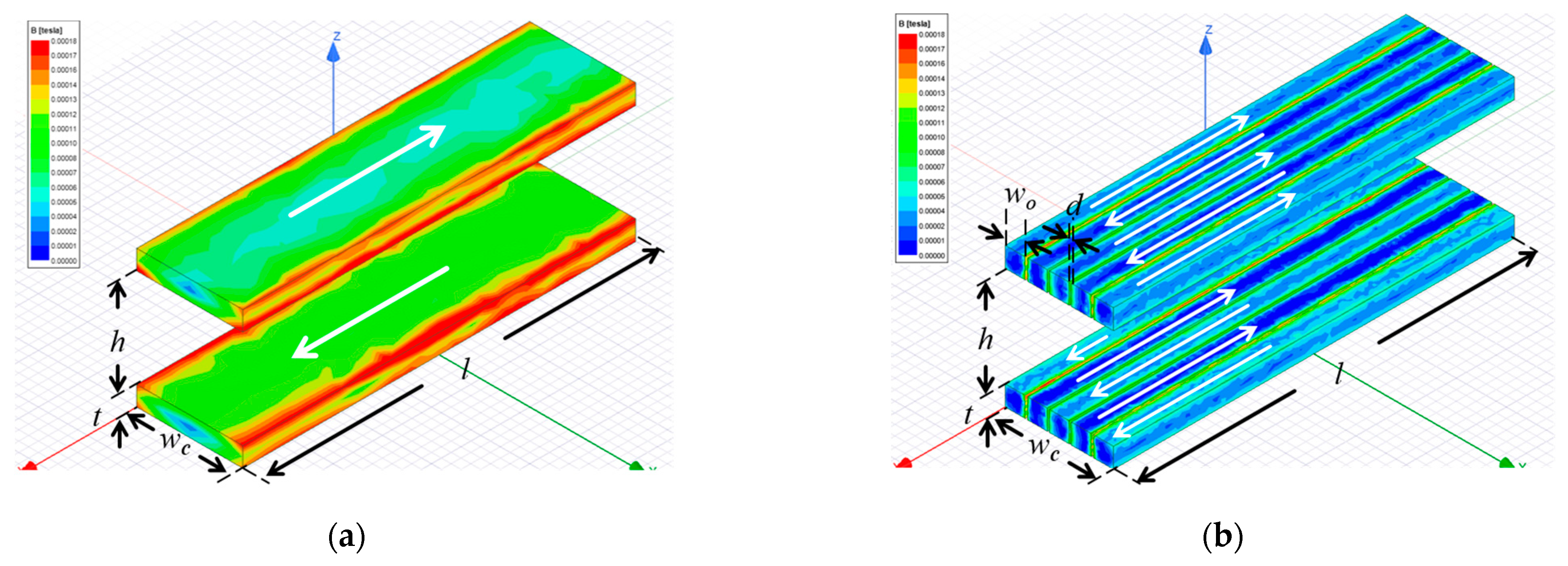
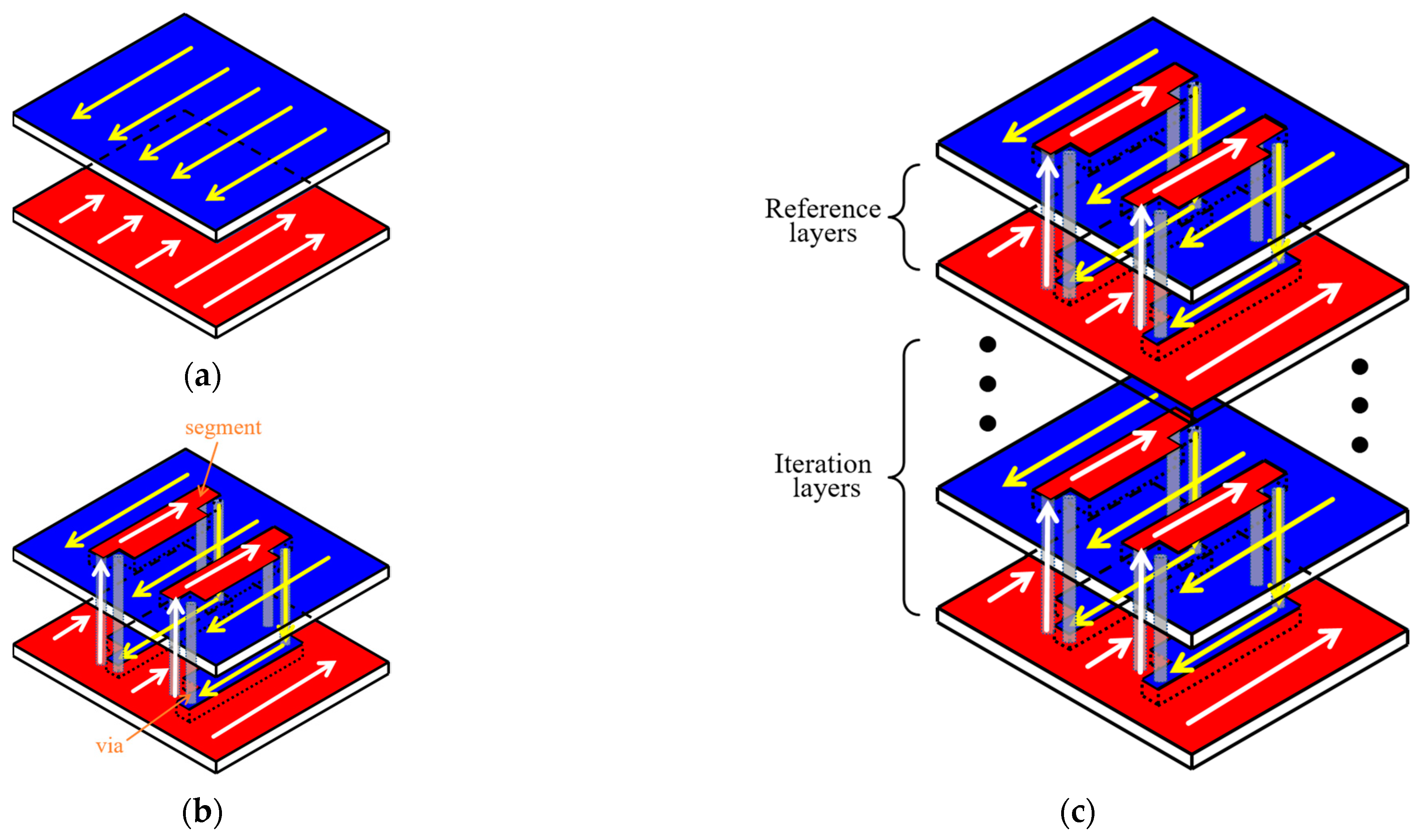
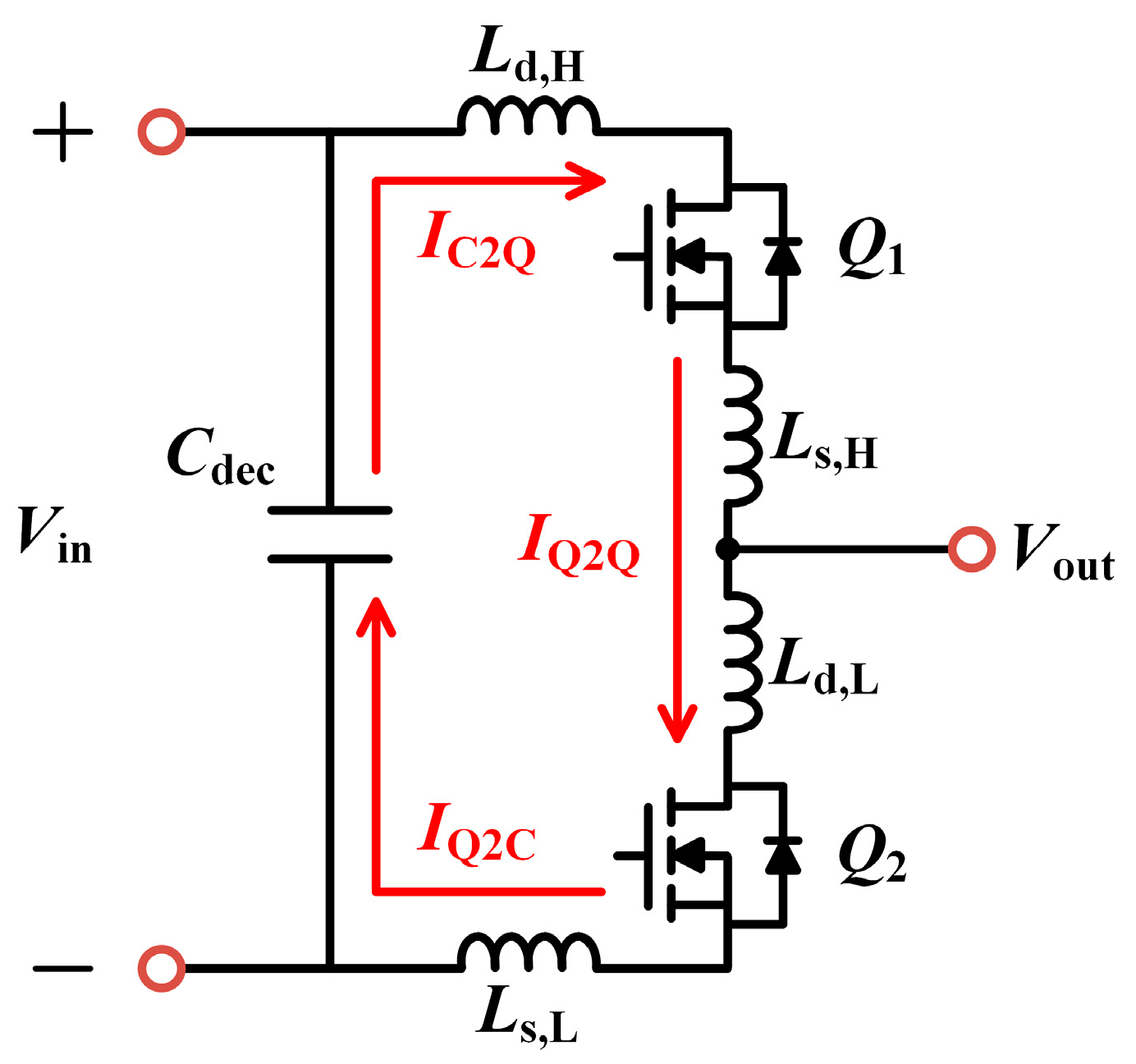
2.2. Proposed Three-Dimensional Lattice Structure
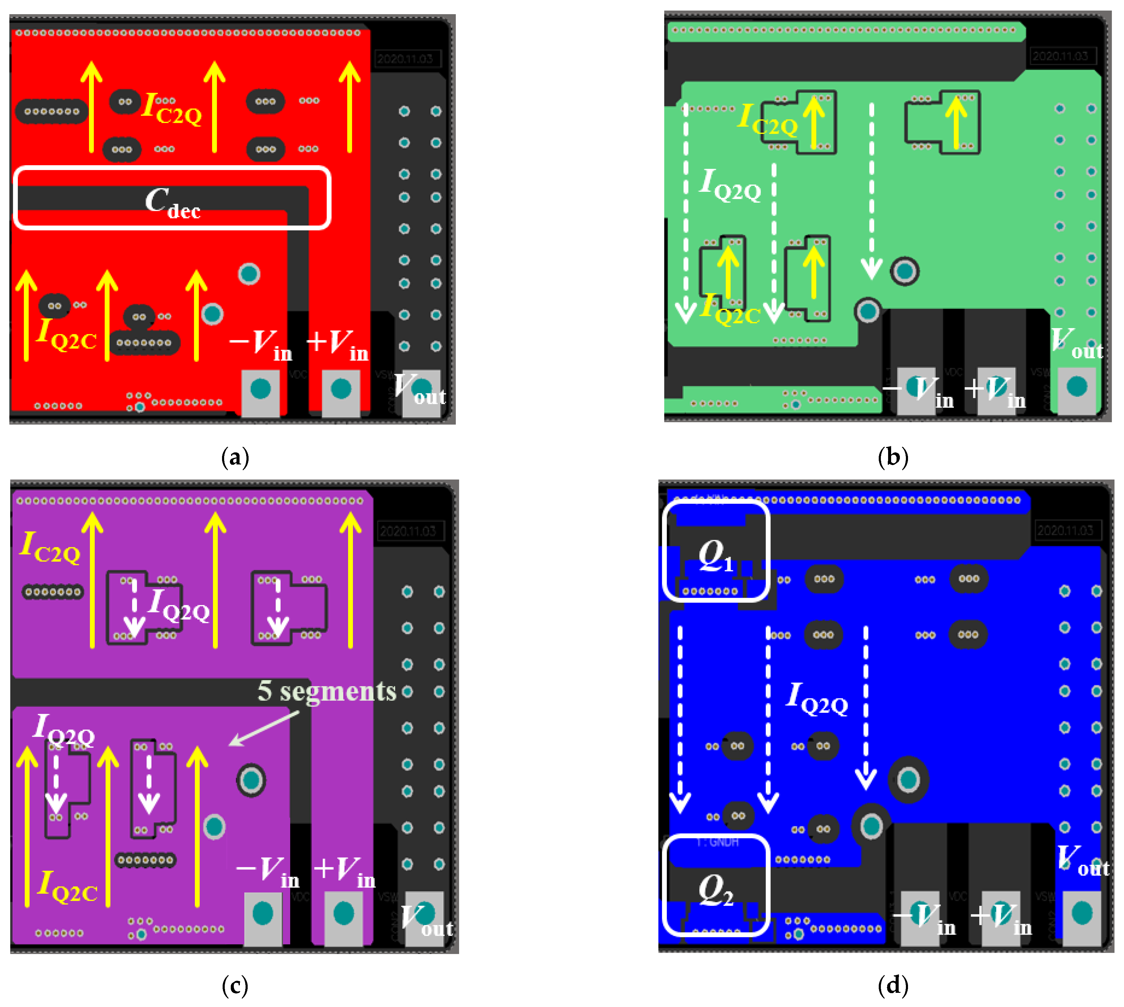
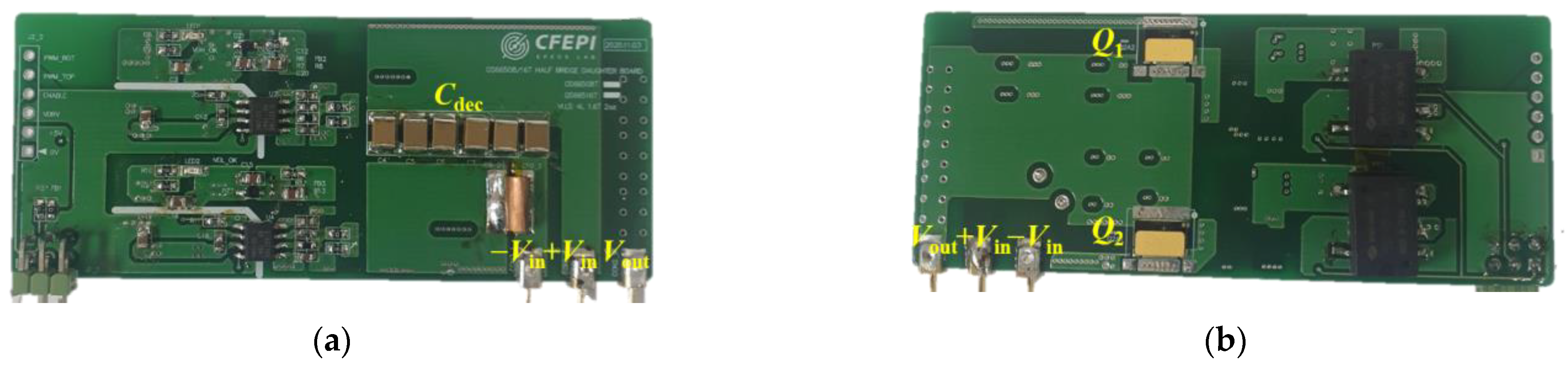
3. Detailed PCB Layout Design of Proposed Three-Dimensional Lattice Structure
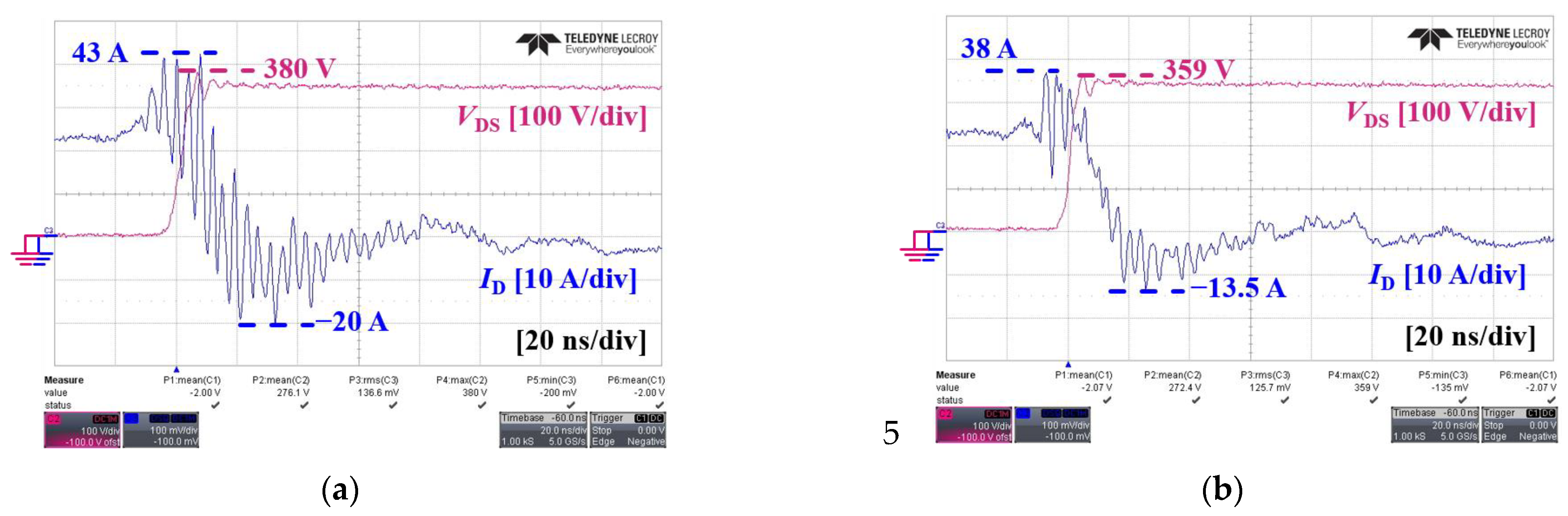
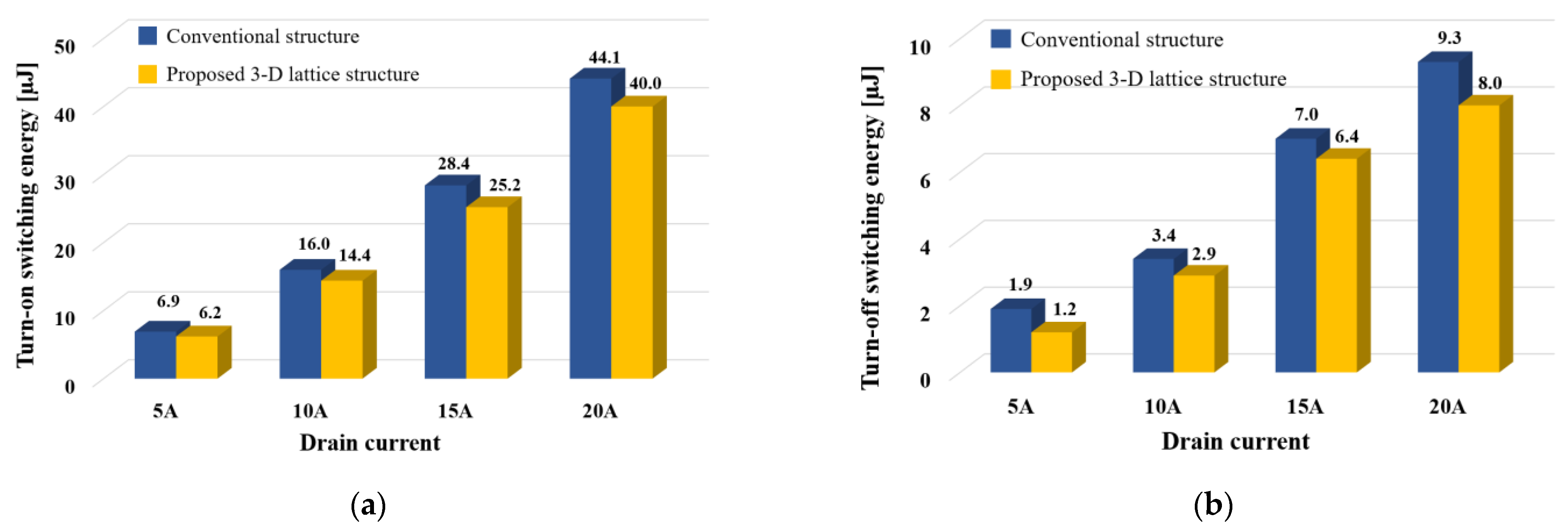
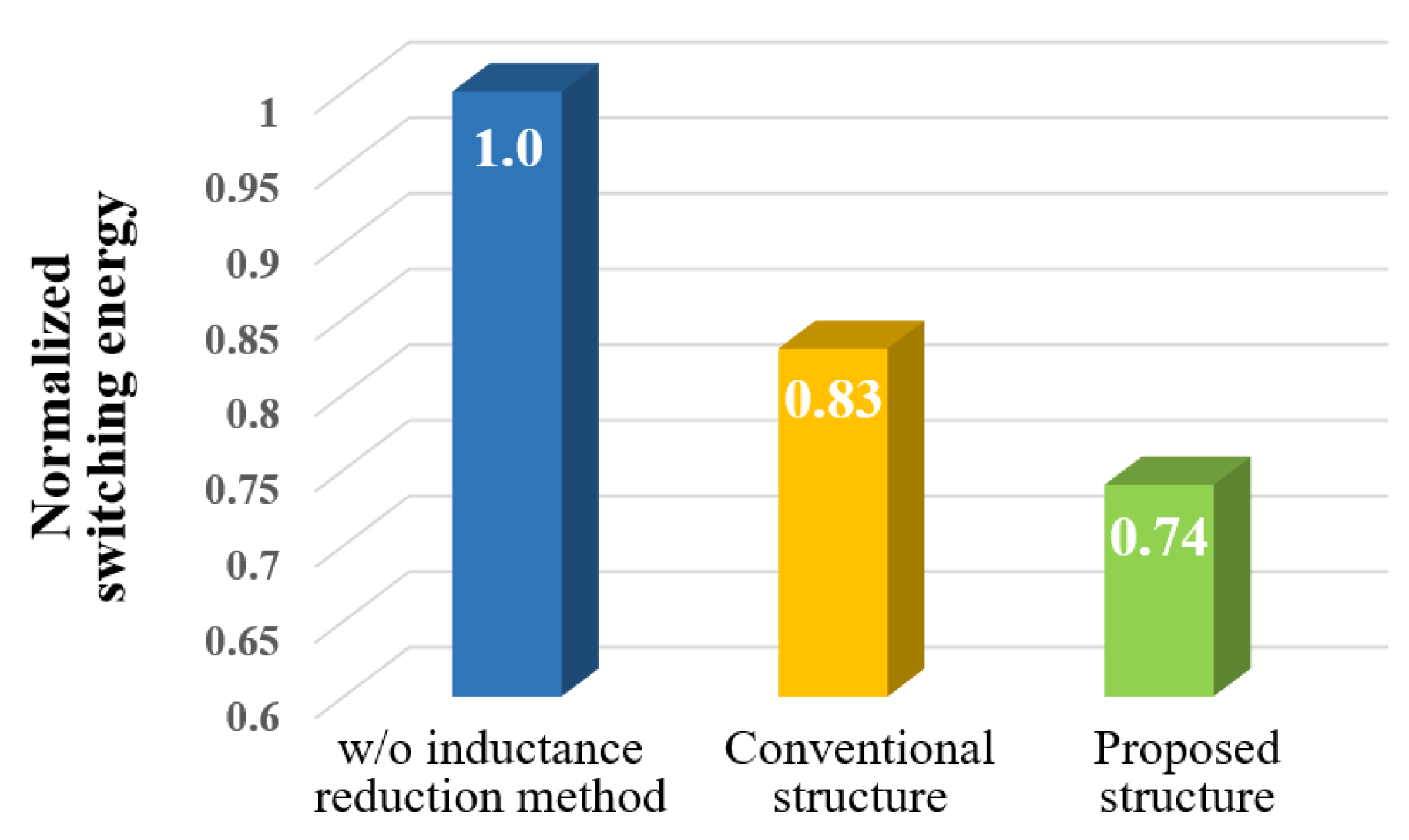
4. Performance Verification
5. Conclusions
Author Contributions
Funding
Data Availability Statement
Conflicts of Interest
References
- Millán, J.; Godignon, P.; Perpiñà, X.; Pérez-Tomás, A.; Rebollo, J. A Survey of Wide Bandgap Power Semiconductor Devices. IEEE Trans. Power Electron. 2014, 29, 2155–2163. [Google Scholar] [CrossRef]
- Lee, F.C.; Li, Q. High-Frequency Integrated Point-of-Load Converters: Overview. IEEE Trans. Power Electron. 2013, 28, 4127–4136. [Google Scholar] [CrossRef]
- Van Wyk, J.D.; Lee, F.C. On a Future for Power Electronics. IEEE J. Emerg. Sel. Top. Power Electron. 2013, 1, 59–72. [Google Scholar] [CrossRef]
- Hudgins, J.L. Power Electronic Devices in the Future. IEEE J. Emerg. Sel. Top. Power Electron. 2013, 1, 11–17. [Google Scholar] [CrossRef]
- Wang, X.; Wang, Z.; Li, M.; Tu, L.; Wang, K.; Xiao, D.; Guo, Q.; Zhou, M.; Wei, X.; Shi, Y.; et al. A New Dibenzoquinoxalineimide-Based Wide-Bandgap Polymer Donor for Polymer Solar Cells. Polymers 2022, 14, 3590. [Google Scholar] [CrossRef] [PubMed]
- Xiao, Y.; Shah, H.; Chow, T.P.; Gutmann, R.J. Analytical modeling and experimental evaluation of interconnect parasitic inductance on MOSFET switching characteristics. In Proceedings of the Nineteenth Annual IEEE Applied Power Electronics Conference and Exposition, Anaheim, CA, USA, 22–26 February 2004. [Google Scholar]
- Pavier, M.; Sawle, A.; Woodworth, A.; Monteiro, R.; Chiu, J.; Blake, C. High frequency DC:DC power conversion: The influence of package parasitics. In Proceedings of the Eighteenth Annual IEEE Applied Power Electronics Conference and Exposition, Miami Beach, FL, USA, 9–13 February 2003. [Google Scholar]
- Wang, J.; Chung, H.S.-h.; Li, R.T.-h. Characterization and Experimental Assessment of the Effects of Parasitic Elements on the MOSFET Switching Performance. IEEE Trans. Power Electron. 2013, 28, 573–590. [Google Scholar] [CrossRef]
- Wang, K.; Yang, X.; Li, H.; Ma, H.; Zeng, X.; Chen, W. An Analytical Switching Process Model of Low-Voltage eGaN HEMTs for Loss Calculation. IEEE Trans. Power Electron. 2016, 31, 635–647. [Google Scholar] [CrossRef]
- Hashimoto, T.; Kawashima, T.; Uno, T.; Akiyama, N.; Matsuura, N.; Akagi, H. A System-in-Package (SiP) With Mounted Input Capacitors for Reduced Parasitic Inductances in a Voltage Regulator. IEEE Trans. Power Electron. 2010, 25, 731–740. [Google Scholar] [CrossRef]
- Ball, A.; Lim, M.; Cilham, D.; Lee, F.C. System design of a 3D integrated non-isolated Point of Load converter. In Proceedings of the 2008 Twenty-Third Annual IEEE Applied Power Electronics Conference and Exposition, Austin, TX, USA, 24–28 February 2008. [Google Scholar]
- Nielsen, J.; Ramachandran, R.; Nymand, M. Demonstration of Ultra Low Loop Inductance on a High Efficient GaN Converter Using PCB Embedded Capacitors. In Proceedings of the 2021 23rd European Conference on Power Electronics and Applications, Ghent, Belgium, 6–10 September 2021. [Google Scholar]
- Qi, Z.; Pei, Y.; Wang, L.; Yang, Q.; Wang, K. A Highly Integrated PCB Embedded GaN Full-Bridge Module with Ultralow Parasitic Inductance. IEEE Trans. Power Electron. 2022, 37, 4161–4173. [Google Scholar] [CrossRef]
- Lu, S.; Zhao, T.; Zhang, Z.; Ngo, K.D.T.; Burgos, R.; Lu, G.-Q. Low Parasitic-Inductance Packaging of a 650 V/150 A Half-Bridge Module Using Enhancement-Mode Gallium-Nitride High Electron Mobility Transistors. IEEE Trans. Ind. Electron. 2023, 70, 344–351. [Google Scholar] [CrossRef]
- Reusch, D.; Lee, F.C.; Gilham, D.; Su, Y. Optimization of a high density gallium nitride based non-isolated point of load module. In Proceedings of the 2012 IEEE Energy Conversion Congress and Exposition (ECCE), Raleigh, NC, USA, 15–20 September 2012. [Google Scholar]
- Reusch, D.; Strydom, J. Understanding the Effect of PCB Layout on Circuit Performance in a High-Frequency Gallium-Nitride-Based Point of Load Converter. IEEE Trans. Power Electron. 2014, 29, 2008–2015. [Google Scholar] [CrossRef]
- Ibuchi, T.; Funaki, T. A study on parasitic inductance reduction design in GaN-based power converter for high-frequency switching operation. In Proceedings of the 2017 International Symposium on Electromagnetic Compatibility, Angers, France, 4–8 September 2017. [Google Scholar]
- Wang, K.; Wang, L.; Yang, X.; Zeng, X.; Chen, W.; Li, H. A Multiloop Method for Minimization of Parasitic Inductance in GaN-Based High-Frequency DC–DC Converter. IEEE Trans. Power Electron. 2017, 32, 4728–4740. [Google Scholar] [CrossRef]
- Dechant, E.; Seliger, N.; Kennel, R. Design of a Low Multi-Loop Inductance Three Level Neutral Point Clamped Inverter with GaN HEMTs. In Proceedings of the 2020 IEEE Energy Conversion Congress and Exposition, Detroit, MI, USA, 11–15 October 2020. [Google Scholar]
- Hammer, J.; Zurbriggen, I.G.; Ali Saket, M.; Ordonez, M. Low Inductance PCB Layout for GaN Devices: Interleaving Scheme. In Proceedings of the 2021 IEEE Applied Power Electronics Conference and Exposition, Phoenix, AZ, USA, 14–17 June 2021. [Google Scholar]
- Yang, S.-S.; Min, S.-S.; Eom, C.-H.; Kim, R.-Y.; Lee, G.-Y. Design Method of Vertical Lattice Loop Structure for Parasitic Inductance Reduction in a GaN HEMTs-Based Converter. IEEE Access 2022, 10, 117215–117224. [Google Scholar] [CrossRef]
- Paul, C.R. Inductance: Loop and Partial; John Wiley & Sons, Inc.: Hoboken, NJ, USA, 2010; pp. 195–245. [Google Scholar]


| w/o Proposed Structure (Figure 4a) | w/Proposed Structure (Figure 4b) | |
|---|---|---|
| Simulated inductance | 98.2 nH | 43.38 nH |
| Parameters | Value |
|---|---|
| Vpk | 650 V |
| Ix | 30 A |
| wc | 18 mm |
| t | 0.07 mm |
| ∆T | 15 °C |
| d | 0.625 mm |
| m | 5 |
| wo | 3.1 mm |
| Parameters | Conventional Structure in [21] | Proposed Structure |
|---|---|---|
| Ld,H | 2.13 nH | 1.69 nH |
| Ls,H | 0.815 nH | 0.615 nH |
| Ld,L | 2.445 nH | 1.845 nH |
| Ls,L | 5.46 nH | 4.11 nH |
| Ltot | 10.85 nH | 8.26 nH |
| Parameters | Value |
|---|---|
| VDC | 300 V |
| ID | 21 A |
| VGS | 6/−3 V |
| Lload | 200 µH |
Disclaimer/Publisher’s Note: The statements, opinions and data contained in all publications are solely those of the individual author(s) and contributor(s) and not of MDPI and/or the editor(s). MDPI and/or the editor(s) disclaim responsibility for any injury to people or property resulting from any ideas, methods, instructions or products referred to in the content. |
© 2023 by the authors. Licensee MDPI, Basel, Switzerland. This article is an open access article distributed under the terms and conditions of the Creative Commons Attribution (CC BY) license (https://creativecommons.org/licenses/by/4.0/).
Share and Cite
Min, S.-S.; Eom, C.-H.; Jang, Y.-S.; Kim, R.-Y. Three-Dimensional Lattice Structure to Reduce Parasitic Inductance for WBG Power Semiconductor-Based Converters. Electronics 2023, 12, 1779. https://doi.org/10.3390/electronics12081779
Min S-S, Eom C-H, Jang Y-S, Kim R-Y. Three-Dimensional Lattice Structure to Reduce Parasitic Inductance for WBG Power Semiconductor-Based Converters. Electronics. 2023; 12(8):1779. https://doi.org/10.3390/electronics12081779
Chicago/Turabian StyleMin, Sung-Soo, Chan-Hyeok Eom, Yeong-Seop Jang, and Rae-Young Kim. 2023. "Three-Dimensional Lattice Structure to Reduce Parasitic Inductance for WBG Power Semiconductor-Based Converters" Electronics 12, no. 8: 1779. https://doi.org/10.3390/electronics12081779
APA StyleMin, S.-S., Eom, C.-H., Jang, Y.-S., & Kim, R.-Y. (2023). Three-Dimensional Lattice Structure to Reduce Parasitic Inductance for WBG Power Semiconductor-Based Converters. Electronics, 12(8), 1779. https://doi.org/10.3390/electronics12081779