Communication

Analysis of a p-i-n Diode Circuit at Radio Frequency Using an Electromagnetic-Physics-Based Simulation Method

College of Electronics and Information Engineering, Sichuan University, Chengdu 610064, China
*
Author to whom correspondence should be addressed.
Electronics 2023, 12(7), 1525; https://doi.org/10.3390/electronics12071525
Submission received: 22 February 2023 / Revised: 21 March 2023 / Accepted: 22 March 2023 / Published: 23 March 2023

Abstract

:
Embracing the era of higher operating frequencies, expanding functionality, and increased integration scale, modern circuit design relies more and more on the accurate prediction of the electromagnetic (EM) effects resulting from undesired radiation and mutual coupling of digital electronic devices. In this paper, an electromagnetic-physics-based simulation method is proposed, to simulate semiconductor devices and circuits. It utilizes physics-based simulation to analyze semiconductor devices in a circuit and incorporates this physics-based simulation into electromagnetic simulation (e.g., the finite difference time domain (FDTD)), to simulate a circuit at high frequency. To validate the proposed method, sample numerical results on circuits containing a commercial p-i-n diode with model number mot_bal99lt1 at radio frequency (RF) were obtained and compared with measurement data. The comparison showed a good agreement between the two sets of data, which validated the feasibility and accuracy of the proposed algorithm. Moreover, the proposed method can provide a useful physical mechanism for understanding effects on semiconductor devices and circuits.

1. Introduction

With the development of modern communication and industry, more and more electrical equipment works at a high frequency, such as RF, which is in the range of about 300 kHz to 30 GHz. The higher operating frequencies, as well as expanding functionality and increased integration scale, place new demands on RF circuits designers. This is especially true in the design of printed circuit boards (PCBs) with semiconductor devices within a packaging structure [1,2]. For example, the modeling of the interaction between traveling waves and charge carriers present in any semiconductor device when its dimensions are comparable to the signal wavelength at the operating frequency. As more active and/or passive devices are integrated on circuit boards, this necessitates the application of full-wave solvers, to ensure accurate prediction of the EM responses of the integrated and packaged components and systems. Hence, accurate simulation is becoming increasingly important for understanding the basic properties of advanced devices, for the prediction of their performance, and for the optimization of their structure, for reduced fabrication effort [3,4].
Researchers have devoted significant efforts to developing various techniques, which are based on different approaches and with varying degrees of accuracy and complexity [3,4,5,6,7,8,9]. On the one hand, the most rigorous approach is the global modeling method, in which the device equations and Maxwell’s equations are solved as a system representing a strongly coupled highly nonlinear set of differential equations on the same grid [5,6]. However, the global modeling method is very complicated, and its execution is time-consuming compared with circuit simulation. Hence, until now, it has only been used to simulate semiconductor devices or, at most, a simple circuit consisting of a semiconductor device and a few other elements. On the other hand, within the framework of the usual circuit-analysis techniques, each element of the physical circuit (an active semiconductor device, as well as a section of the interconnecting line) is described by an equivalent circuit; the simulation thus relies on a library of topologies and technological parameters, which need to be characterized with respect to the actual fabrication process [7,8,9]. However, the equivalent circuit may lose accuracy in some special cases, such as high-power or high-frequency applications; moreover, most of them lack a direct physical interpretation [7]. For example, it is mentioned in the literature that the simulation of a simple circuit containing a PIN diode using ADS at 20 MHz did not show the phenomenon of “punch-through” current, which is not consistent with experiments [10]. Among the available techniques, a hybrid solver that combines the capabilities of a physics-based simulation and a full-wave analysis has attracted researchers’ interest, particularly because of its ability to account for the presence of lumped components in a distributed circuit [10,11,12,13,14,15,16]. This is based on semiconductor device physical models, rather than equivalent models, and solves field equations such as the Maxwell equations, semiconductor transport equations, and thermodynamics equations, to model the electromagnetic wave propagation and charge transport with the temperature effects inside semiconductor devices. Hence it is able to accurately simulate semiconductor devices under various conditions and is convenient for predicting physical effects. Meanwhile, the EM effect can be achieved using a full-wave approach, which includes the effect through solving Maxwell’s equations and comprehensively taking into account the interaction between the electromagnetic waves and circuit elements.
This work introduces an electromagnetic-physics-based simulation method, in which physics-based simulation is employed for analyzing the crucial and sensitive semiconductor devices, and then the active devices are placed on the edges of the FDTD grid, working as n-terminal lumped elements, in order to be directly incorporated into Yee’s algorithm based on the quasi-static assumption, in which the dimension of the active region is well below the wavelength of the propagating signal. Since physics-based circuit simulation is based on a physical model, it is naturally able to accurately simulate the behavior of semiconductor devices under various conditions, and it can be used for predicting physical effects. Meanwhile, a discretization grid that is independent of the FDTD mesh is adopted for the physical model of the p-i-n diode, which can avoid employing physics-based simulation to analyze the propagation of electromagnetic fields along the “passive” circuit domain (including the package and other environmental factors, if needed) in the whole circuit at a high frequency, greatly reducing the computation burden.
The proposed method was applied to analyze a circuit comprising a commercial p-i-n diode of model mot_bal99lt. Then, a series of experiments were conducted to validate the proposed method. The remainder of this paper is organized as follows: The proposed electromagnetic-physics-based method is formulated in Section 2. Then, in Section 3, the simulation results of the high frequency effect on p-i-n diodes circuits are presented and compared with measurement data. Finally, the conclusions are drawn in Section 4.

2. Principle of the Electromagnetic- Physics-Based Method

2.1. The Physics-Based Circuit Simulation

In principle, the behavior of semiconductors can be described using a multi-physics equation system [17], which includes Poisson’s Equation (1), the continuity equations for electrons (2) and holes (3), the current relations for electrons (4) and holes (5), and the branch current Equation (6). In the equation system, Poisson’s Equation (1) is a simplification of the Maxwell equations after adopting “lumped” assumption [8], and the continuity and current Equations (2)–(5) are derived from the Boltzmann transport theory by employing drift–diffusion approximation [18].
2 φ = - q ε ( p - n + N t )
n t = 1 q J n - R
p t = - 1 q J p - R
J n = q D n n + q μ n n φ
J p = q D p p + q μ p p φ
I j = ( J n + J p + ε E t ) A δ
where ε is the permittivity, φ is the electrostatic potential, Nt is doping density, n is electron density, q is the elementary charge, p is the hole density, t is time, Jn and Jp are the electron and hole current density, R represents the electro-hole recombination rates, Dn and Dp are the corresponding diffusion coefficients, μn and μp are the electron and hole mobility, I is the branch current, E is the electric field intensity, A is the cross-sectional area, and δ is a unit vector normal to the cross-section.
The difference method is used to differentially discretize the current continuity equation and Poisson’s equation, and the differential equation of current density is substituted into the current continuity equation. Since the equations are nonlinear, a linearization process is required to linearize through Taylor expansion, neglecting the higher terms above the quadratic level to obtain the iterative form as
A Δ y ( k - 1 ) + B Δ y ( k ) + C Δ y ( k + 1 ) = H ( k )
where y = [φ n p]T, Δy = [Δφ Δn Δp]T; A, B, and C are 3 × 3 matrixes; and H is a 3 × 1 matrix.
Assuming a device is located in the jth branch and between the (k − 1)th and the kth node in a circuit, the relationship between its node voltages (Uk−1 and Uk) and branch current can be described as
I j = ψ ( U k , U k - 1 )
To simplify the simulation and reduce the computational burden, in the proposed method, crucial and sensitive semiconductors in a circuit are simulated using the above-introduced physical-based field simulation; as for other devices, Equation (8) is derived from their equivalent circuit models [19].
Using the Newton–Raphson algorithm and two trial solutions  U k 1 Δ  and  U k Δ  to approximately calculate the partial derivatives of Ij, the simulation of a circuit can be simplified to the solution of an increment equation
U n + 1 = U n - [ f 1 n U 1 n f 1 n I j n Δ 1 + f 1 n U k - 1 n f 1 n I j n Δ 2 + f 1 n U k n f 2 n U 1 n f 2 n I j n Δ 1 + f 2 n U k - 1 n f 2 n I j n Δ 2 + f 2 n U k n f k n U 1 n f k n I j n Δ 1 + f k n U k - 1 n f k n I j n Δ 2 + f k n U k n ] - 1 f ( U n )
in which,  U = [ U 1 , U 2 , , U k ] T f ( U ) = [ f 1 ( U ) , f 2 ( U ) , , f k ( U ) ] T U k - 1 n Δ = U k - 1 n + Δ Δ 1 = ψ ( U k - 1 n Δ , U k n ) - ψ ( U k - 1 n , U k n ) U k - 1 n Δ - U k - 1 n Δ 2 = ψ ( U k - 1 n , U k n Δ ) - ψ ( U k - 1 n , U k n ) U k n Δ - U k n  where k is the index of the unknown node, fk(U) is the nodal equation, n is the iteration index, and Δ is a small constant selected based on experience for a convergent solution.

2.2. Electromagnetic-Physics-Based Simulation

For a circuit working at a high frequency, successful circuit design requires the inclusion of the electromagnetic effects. This requirement can be fulfilled by a full-wave approach, which includes the effect through solving Maxwell’s equations and comprehensively taking into account the interaction between the electromagnetic waves and circuit elements [19,20]. To simulate semiconductor devices and circuits at a high frequency, the extension of the FDTD method is adopted in this paper. Let us refer, for the sake of simplicity, to a two-terminal semiconductor device, lumped at the connecting nodes (a and b) along the x-axis, as depicted in Figure 1.
In the present implementation, a 1-D discretization grid is adopted for the physical model of the semiconductor device, which is fully independent of the 3-D-FDTD mesh. For the physical model, space-domain integration of the semiconductor device current equations relies on the well-known Scharfetter–Gummel scheme [21], whereas a backward-Euler algorithm [22] is adopted to accomplish time-domain integration. Based on the assumption of a quasi-stationary approximation holding for active devices; i.e., the size of device active regions is assumed to be negligible, with respect to the minimum signal wave-length, the device can therefore be regarded, when solving Maxwell’s equations, as a “lumped” (i.e., zero-dimensional) element, while the dielectric constant in the device region is assumed to be that of air, and thus Maxwell’s equations, including a semiconductor device, in integral form, can be described as:
c Ε d l = s μ H t d s
c H d l = s σ E d s + s ε E t d s + I s
where Is is the total current flowing through the integral surface from the semiconductor device.
Using an implicit scheme for the current from the circuit, the relation between electric field  E α n + 1  and lumped current  I s α n + 1  ( α = x , y , z ) can be obtained, the component of the current integration Equation (11) can be rewritten as
E x ( i , j , k ) n + 1 = ε ( i , j , k ) d t σ ( i , j , k ) 2 ε ( i , j , k ) d t + σ ( i , j , k ) 2 E x ( i , j , k ) n + 1 ε ( i , j , k ) d t + σ ( i , j , k ) 2 ( H z ( i , j , k ) n + 1 2 H z ( i , j - 1 , k ) n + 1 2 d y H y ( i , j , k ) n + 1 2 H z ( i , j , k - 1 ) n + 1 2 d z I s n + 1 d y d z )
The voltage drop across the semiconductor device is obtained as
V a b n + 1 = ( i b , j b , k b ) ( i a , j a , k a ) E x ( i , j , k ) n + 1 d x
Applying path integration between point a and point b to both sides of Equation (11), it can be rewritten as
( I x n + 1 ) E M = V a b n + 1 ( R x n + 1 ) g r i d + I s n + 1
the equivalent resistance Rgrid and the equivalent current IEM are defined as
( R x n + 1 ) g r i d = 1 ( ε ( i , j , k ) d t + σ ( i , j , k ) 2 ) d y d z β = ( i b , j b , k b ) β = ( i a , j a , k a ) d x
( I s n + 1 ) E M = β = ( i b , j b , k b ) β = ( i a , j a , k a ) d x Κ x i j k n + 1 ( R x n + 1 ) g r i d
in which
Κ x i j k n + 1 = ε ( i , j , k ) d t - σ ( i , j , k ) 2 ε ( i , j , k ) d t + σ ( i , j , k ) 2 E x ( i , j , k ) n + 1 ε ( i , j , k ) d t + σ ( i , j , k ) 2 ( H z ( i , j , k ) n + 1 2 - H z ( i , j - 1 , k ) n + 1 2 d y - H y ( i , j , k ) n + 1 2 - H z ( i , j , k - 1 ) n + 1 2 d z )
Hence, an equivalent subcircuit consisting of a resistor Rgrid and a current source IEM is added to the circuit simulation by Equation (14) and the lumped current Is, in return, is fed back to the field iteration using Equation (12) in the node containing the semiconductor device. The data flow between the different blocks is shown in Figure 2. In this way, the physical-model circuit simulation and the FDTD field simulation are integrated into a unified scheme. The algorithm can be summarized as follows:
(1)
Initialize the parameters such as the doping profile and bias voltage, use physics-based circuit simulation to solve for the initial values of n, p, and Is.
(2)
Apply excitation
(3)
Select the largest time-step dt which ensures both FDTD stability and physics-based circuit simulation convergence;
(4)
Update the magnetic field H at time t + 0.5 from Equation (10);
(5)
Apply magnetic field H boundary conditions;
(6)
Update the electric field E components at time t + 1 from Equation (11);
(7)
Evaluate n, p, and Is at time t + 1 at device insertion cells using the physics-based circuit simulation from Equation (14);
(8)
Apply electric field E boundary conditions;
(9)
Repeat steps 2–8, using the updated time t = t + 1, until reaching a convergence criterion, which can be defined as the total time required by the simulation.

3. Results of the Application of the Proposed Method

In this section, the proposed method was employed for the analysis of RF circuits loaded with a commercial p-i-n diode with model number mot_bal99lt1. To validate the proposed method, the results were compared with experimental data.

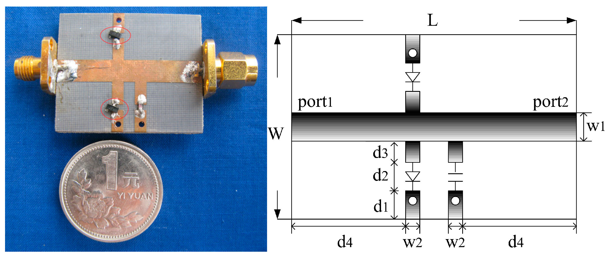
3.1. The Physical Model of the Mot_bal99lt1 p-i-n Diodes and Its Parameters

The physical model of a p-i-n diode is shown in Figure 3. In general, the doping profile of a p-i-n diode can be described by [21]
N t ( x ) = N b [ 1 - ( N a / N b ) v 1 + ( N d / N b ) v 2 ]
in which  v 1 1 ( x / X a ) 2 v 2 1 [ ( w - x ) / X d ] 2 , and  w = X a + X b + X d ; Xa, Xb, and Xd are the thickness of p-layer, i-layer, and n-layer; and Na, Nb, and Nd are the doping concentrations.
The p-i-n diode was mounted in series configuration and encapsulated in an SOT23 package with three leads. In the high-frequency range, the package parasitic parameters (see Figure 4a) must be considered [23]. To extract the physical parameters of the p-i-n diode, a diode was mounted across a 50 Ω microstrip line gap (see Figure 4b), and its S-parameter was measured (see Figure 4c). By employing a GA-based curve-fitting approach and from the measured data, the physical parameters of the mot_bal99lt1 p-i-n diode were extracted, as follows: the life time τp0 = 5 × 10⁻⁹ s and τn0 = 5 × 10⁻⁹ s for p-type and n-type carriers, Xa = 5 μm, Xb = 1.55 μm, Xd = 0.5 μm, Na = 1.8 × 10¹⁶/cm3, Nb = 0.5 × 10¹⁰/cm3, Nd = 1.8 × 10¹⁶/cm3, the cross-sectional area A = 0.7 cm2, the chip resistance R = 0.5 Ω, the wire inductance L1 = 0.25 nH, the lead inductance L2 = 0.15 nH, and the package capacitance C = 0.39 pF.

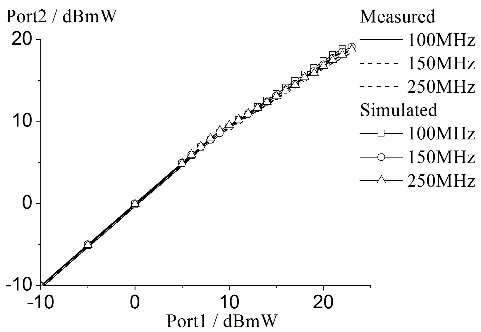
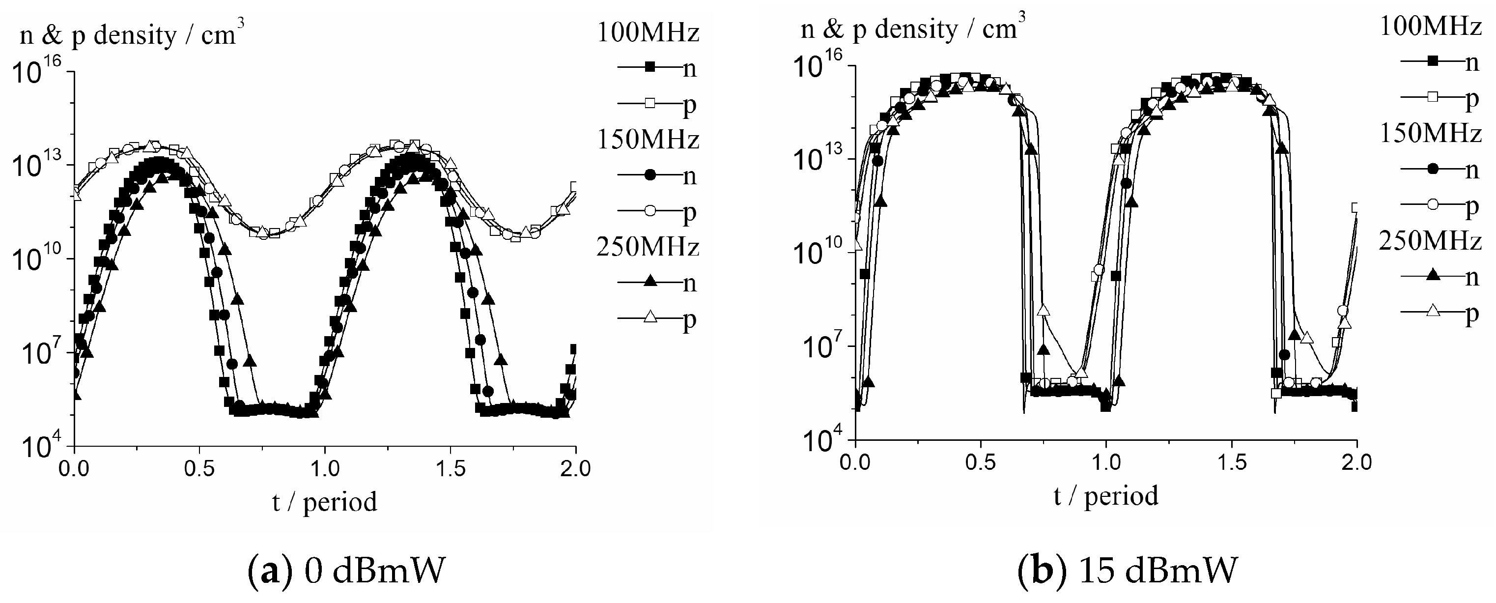
3.2. Power Limiting Characteristics of a p-i-n Diode at RF

A p-i-n diode circuit (see Figure 5) was fabricated on a PCB (printed circuit board) with relative dielectric constant εr = 2.65 and thickness h = 2 mm. In the circuit, a p-i-n diode was series-mounted across a microstrip gap, its N-terminal was connected to the ground via a metal hole, and the width of the conductor was 5.4mm, determined to correspond to the characteristics impedance of 50 Ω. Other structural parameters are marked in Figure 5. The power limiting characteristics of the p-i-n diode were simulated using the proposed method. Meanwhile, measurements were carried out using an Agilent E8267C signal source and a power meter.
From the comparison between the simulated and measured results shown in Figure 6, it can be observed that they are in good agreement, which validated the accuracy of the proposed method. In addition, the results illustrate that the circuit exhibited a power limiting characteristic, as the power of the sine signal increased to more than 7 dBmW, e.g., when a sine signal with power of 21 dBmW was fed to port1, the measured and simulated output power in the port2 were as following: (1) the measurement was 17.83 dBmW and the simulation was 18.13 dBmW at100 MHz; (2) the measurement was 17.38 dBmW and the simulation was 17.71 dBmW at 150 MHz; and (3) the measurement was 17.38 dBmW and the simulation was 17.71 dBmW at 250 MHz.
The power limiting characteristics of the circuit could be obtained using the proposed method presented in the previous section. As shown in Figure 7a, when a sine signal with power of 0 dBmW was fed to port1, the carrier concentration inside i-layer of the p-i-n diode was less than 5 × 10¹⁵/cm3 during the whole period. A low-level carrier density means that the diode had a higher volume resistivity, and the total current of the p-i-n diode was mainly determined by the displacement current, as illustrated in Figure 8a, which means that the p-i-n diode may be equivalent to a capacitor in this condition, and finally resulted in the electric field  | E z |  of the port2 being equal to that of the sine signal source, as depicted in Figure 9a; namely, the circuit did not exhibit a limiting characteristic under a small sine signal source. However, the carrier concentration inside the i-layer of the p-i-n diode increased sharply with the signal source power. This was in the order of 3 × 10¹⁵/cm3 during the first half period, when a sine signal with power of 15 dBmW was fed to port1, as depicted in Figure 7b. The high-level carrier density meant that the diode had very good electrical conductivity, and the conduction current, which has a nonlinear variation with the sine signal source power, took the dominant position in the total current of the p-i-n diode, as illustrated in Figure 8b. Hence, the p-i-n diode was equivalent to a nonlinear resistor during the first half period, the electric field  | E z |  of the port2 was less than that of the sine signal source in the first half period, as depicted in Figure 9b, which clearly demonstrates the power limiting characteristic of the circuit.

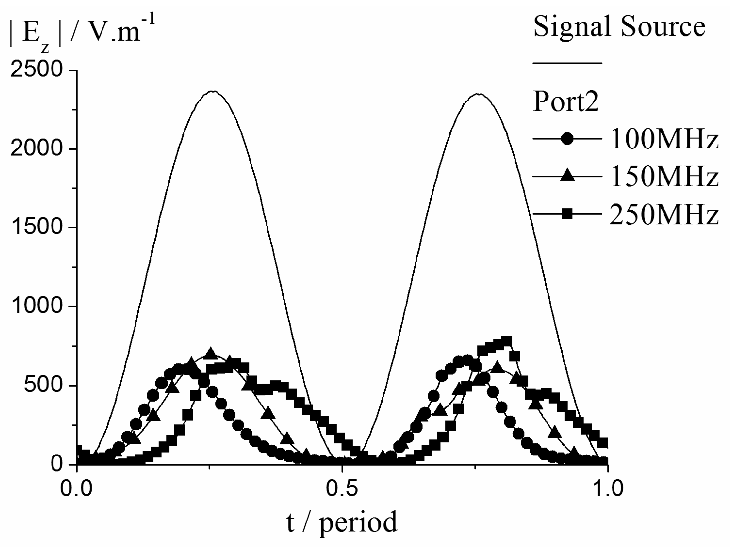
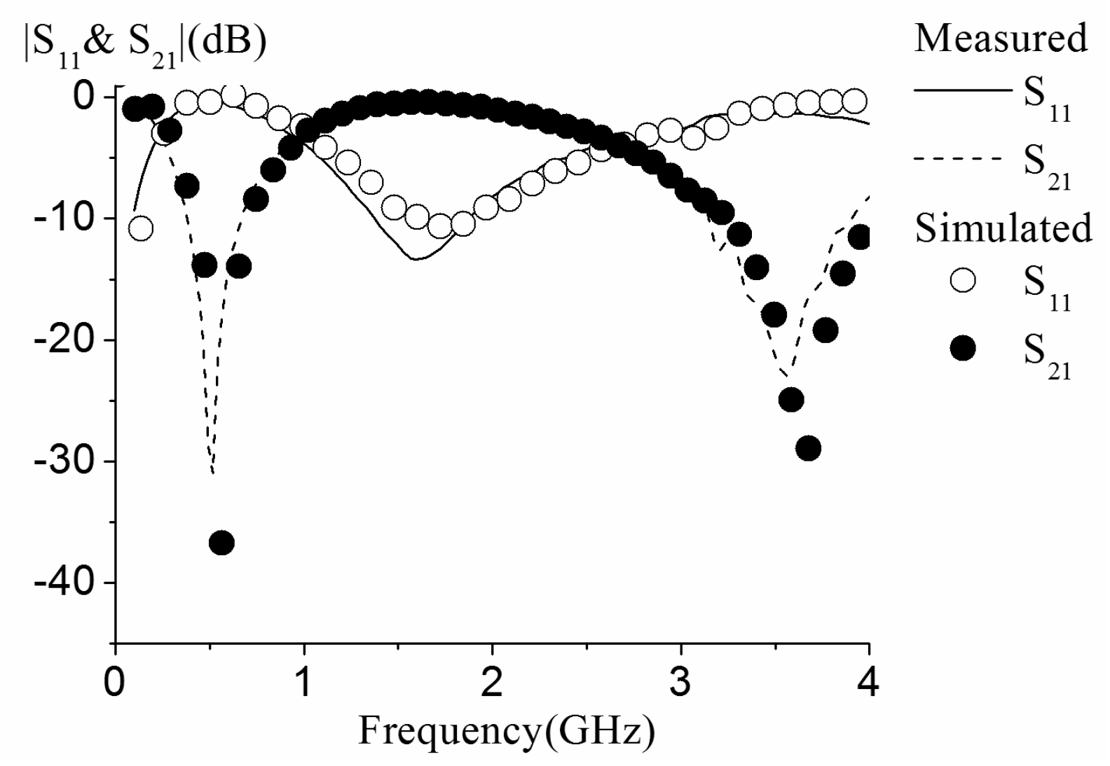
3.3. RF Characteristics of the PIN Diode Limiter

To further demonstrate the capacity and accuracy of the proposed method, it was applied in the analysis of a complex microstrip p-i-n diode limiter, shown in Figure 10, in which two p-i-n diodes and a capacitor CL = 22 pF were series-mounted across microstrip gaps, they were connected to the ground via a metal hole, the width of the conductor w1 = 5.4 mm was determined to correspond to the characteristic impedance of 50 Ω, and the relative dielectric constant and thickness of the PCB were εr = 2.65 and h = 2 mm. Other structural parameters were as follows (unit mm): L = 35.1 mm, W = 29.7 mm, w2 = 2.7 mm, d1 = d3 = 5.4 mm, d2 = 1.35 mm, and d4 = 2.7 mm. The characteristics of the limiter at different frequencies were simulated using the proposed algorithm. Meanwhile, measurement was carried out using an Agilent E8267C signal source and a power meter.
Figure 11 compares the measured and simulated power limiting characteristics of the p-i-n diode limiter at different frequencies. From the comparison, one can observe that the two sets of data are in good agreement, which demonstrated the capacity and accuracy of the proposed algorithm in simulating a relatively complicated circuit. Meanwhile, it also clearly illustrates the limiting characteristic of the limiter under a large sine signal source with a power more than 7 dBm, and the power limiting effect of the limiter was more significant than the simple microstrip circuit with one p-i-n diode. For the limiter, two p-i-n diodes were connected in parallel, so that, at any time, one of them was in turn-on state as a large sine signal source was fed to the port1, which resulted in the electric field  | E z |  of the port2 being less than that of the sine signal source over the whole period, as depicted in Figure 12.
To validate the proposed method using in a higher frequency range, its return loss (S11) and insert loss (S21) were simulated using the proposed method, and the results were compared with those from measurements using an Agilent E8362B Network Analyzer. As depicted in Figure 13, the measured and simulated results were in good agreement, which validated the accuracy of the proposed method, even microwave frequencies.

4. Conclusions

In this paper, an effective electromagnetic-physics-based simulation method was proposed, for analysis of semiconductor devices and circuits. It adopts physical-based circuit simulation to analyze the semiconductor devices in a circuit and incorporates physical-based circuit simulation in field simulation, to realize the complicated effects of semiconductor devices in electromagnetic environments. The proposed method was employed to simulate a circuit containing commercial semiconductors with the model number mot_bal99lt1, and the circuit simulation was validated by comparing the simulation results with measurement data. The simulation results agreed well with the measurement data. Moreover, the proposed algorithm is capable of depicting useful physical pictures for the analysis of semiconductor devices and circuits. These merits make the proposed method a powerful and effective tool for semiconductor device and circuit simulation.

Author Contributions

Conceptualization, Z.C. and X.C.; Funding acquisition, X.C.; Investigation, Z.C. and J.C.; Methodology, Z.C. and J.C.; supervision, X.C.; writing—original draft, Z.C.; writing—review and editing, J.C. and X.C. All authors have read and agreed to the published version of the manuscript.

Funding

This work was supported by National Natural Science Foundation of China (U19A2054).

Data Availability Statement

Not applicable.

Conflicts of Interest

The authors declare no conflict of interest.

References

  1. Bakoglu, H.B. Circuits, Interconnections, and Packaging for VLSI; Addison-Wesley: Reading, MA, USA, 1988. [Google Scholar]
  2. Orhanovic, N.; Matsui, N. Full Wave Signal and Power Integrity Analysis of Printed Circuit Boards Using 2D and 3D FDTD-SPICE Methods. In Proceedings of the High Performance System Design Conference (DesignCon), Santa Clara, CA, USA, 28 January–1 February 2002. [Google Scholar]
  3. Hussein, Y.A.; El-Ghazaly, S.M.; Goodnick, S.M. An efficient electromagnetic-physics-based numerical technique for modeling and optimization of high-frequency multifinger transistors. IEEE Trans. Microw. Theory Tech. 2003, 51, 2334–2346. [Google Scholar] [CrossRef]
  4. Cidronali, A.; Leuzzi, G.; Manes, G.; Giannini, F. Physical/electromagnetic pHEMT modeling. IEEE Trans. Microw. Theory Tech. 2003, 51, 830–838. [Google Scholar] [CrossRef]
  5. Grondin, R.O.; El-Ghazaly, S.M.; Goodnick, S. A review of global modeling of charge transport in semiconductors and full-wave electromagnetics. IEEE Trans. Microw. Theory Tech. 1999, 47, 817–829. [Google Scholar] [CrossRef]
  6. Movahhedi, M.; Abdipour, A. Efficient numerical methods for simulation of high-frequency active devices. IEEE Trans. Microw. Theory Tech. 2006, 54, 2636–2645. [Google Scholar] [CrossRef]
  7. Antoinette, P.; Massobrio, G. Semiconductor Device Modeling with SPICE; McGraw-Hil: New York, NY, USA, 1988. [Google Scholar]
  8. Mantooth, H.A.; Duliere, J.L. A unified diode model for circuit simulation. IEEE Trans. Power Electron. 1997, 12, 816–823. [Google Scholar] [CrossRef]
  9. Yang, S.S.; Kim, T.Y.; Kong, D.K.; Kim, S.S.; Yeom, K.W. A novel analysis of a Ku-band planar p-i-n diode limiter. IEEE Trans. Microw. Theory Tech. 2009, 57, 1447–1460. [Google Scholar] [CrossRef]
  10. Chen, X.; Chen, J.Q.; Huang, K.; Xu, X.B. A Circuit Simulation Method Based on Physical Approach for the Analysis of Mot_bal99lt1 p-i-n Diode Circuits. IEEE Trans. Electron. Devices 2011, 58, 2862–2870. [Google Scholar] [CrossRef]
  11. Wang, R.; Jin, J.M. A Symmetric Electromagnetic-Circuit Simulator Based on the Extended Time-Domain Finite Element Method. IEEE Trans. Microw. Theory Tech. 2008, 56, 2875–2884. [Google Scholar] [CrossRef]
  12. He, Q.; Jiao, D. Fast electromagnetics-based co-simulation of linear network and nonlinear circuits for the analysis of high-speed integrated circuits. IEEE Trans. Microw. Theory Tech. 2010, 58, 3677–3687. [Google Scholar] [CrossRef]
  13. Chen, J.Q.; Chen, X.; Liu, C.J.; Huang, K.; Xu, X.B. Analysis of Temperature Effect on p-i-n Diode Circuits by a Multiphysics and Circuit Cosimulation Algorithm. IEEE Trans. Electron. Devices 2011, 59, 3069–3077. [Google Scholar] [CrossRef]
  14. Chen, S.; Ding, D.; Yu, M.; Wang, Y.; Chen, R. Electro-Thermal Analysis of Microwave Limiter Based on the Time-Domain Impulse Response Method Combined with Physical-Model-Based Semiconductor Solver. IEEE Trans. Microw. Theory Tech. 2020, 68, 2579–2589. [Google Scholar] [CrossRef]
  15. Xu, K.; Chen, X.; Zhang, B.; Chen, Q. A parameter extraction method of the PIN diode for physics-based circuit simulation over a wide frequency range. Int. J. RF Microw. Comput. Aided Eng. 2020, 30, e22385. [Google Scholar] [CrossRef]
  16. Zeng, H.; Chen, X. Nonlinear Analysis for Microwave Limiter Using a Field-Circuit Simulator Based on Physical Models. IEEE Microw. Wirel. Compon. Lett. 2020, 30, 129–132. [Google Scholar] [CrossRef]
  17. Sze, S.M. Physics of Semiconductor Devices; Wiley & Sons: New York, NY, USA, 1981. [Google Scholar]
  18. Xu, X.S. A drift-diffusion model for semiconductors with temperature effects. Proc. R. Soc. Edinb. Sect. A 2009, 139, 1101–1119. [Google Scholar] [CrossRef]
  19. Sui, W. Time-Domain Computer Analysis of Nonlinear Hybrid System; CRC Press: Boca Raton, FL, USA, 2002. [Google Scholar]
  20. Piket-May, M.; Taflove, A.; Baron, J. FDTD modeling of digital signal propagation in 3-D circuits with passive and active loads. IEEE Trans. Microw. Theory Tech. 1994, 42, 1514–1523. [Google Scholar] [CrossRef]
  21. Scharfetter, D.L.; Gummel, H.K. Large-signal analysis of a silicon read diode oscillator. IEEE Trans. Electron. Devices 1969, ED-16, 64–77. [Google Scholar] [CrossRef]
  22. Bank, R.; Coughran, W.; Fichtner, W.; Rose, D.; Smith, R. Computational aspects of semiconductor device simulation. In Process and Device Modeling; Engl, W.L., Ed.; North Holland: Amsterdam, The Netherlands, 1986. [Google Scholar]
  23. Emili, G.; Alimenti, F.; Mezzanotte, P.; Roselli, L.; Sorrentino, R. Rigorous modeling of packaged schottky diodes by the nonlinear lumped network (NL2N)-FDTD approach. IEEE Trans. Microw. Theory Tech. 2000, 48, 2277–2282. [Google Scholar] [CrossRef]
Figure 1. Discretization cell according to Yee’s field-mapping notation.
Electronics 12 01525 g001
Figure 2. Principal of the co-simulation of the circuit effects and EM environment.
Electronics 12 01525 g002
Figure 3. The 1-D and 3-D physical models of the p-i-n diode.
Electronics 12 01525 g003
Figure 4. (a) Package parasitic parameters, (b) circuit used to extract physical parameters of the diode, and (c) comparison of the simulated and measured S−parameter.
Electronics 12 01525 g004
Figure 5. The p-i-n diode circuit.
Electronics 12 01525 g005
Figure 6. Simulated and measured power limiting characteristics of the p-i-n diode at different frequencies.
Electronics 12 01525 g006
Figure 7. The simulated carrier concentration inside the center i-layer of the p-i-n diode at different frequencies.
Electronics 12 01525 g007
Figure 8. The simulated current of the p-i-n diode at different frequencies.
Electronics 12 01525 g008
Figure 9. The simulated amplitude of the electric field  | E z |   at port2 at different frequencies.
Electronics 12 01525 g009
Figure 10. A real p-i-n diode limiter circuit and its structure.
Electronics 12 01525 g010
Figure 11. Simulated and measured power limiting characteristics of the p-i-n diode limiter at different frequencies.
Electronics 12 01525 g011
Figure 12. The simulated amplitude of the electric field  | E z |   at port2 at different frequencies, when the power of the signal source was 21 dBmW.
Electronics 12 01525 g012
Figure 13. Measured and simulated S parameters of the p-i-n diode limiter at microwave frequencies.
Electronics 12 01525 g013
Disclaimer/Publisher’s Note: The statements, opinions and data contained in all publications are solely those of the individual author(s) and contributor(s) and not of MDPI and/or the editor(s). MDPI and/or the editor(s) disclaim responsibility for any injury to people or property resulting from any ideas, methods, instructions or products referred to in the content.

