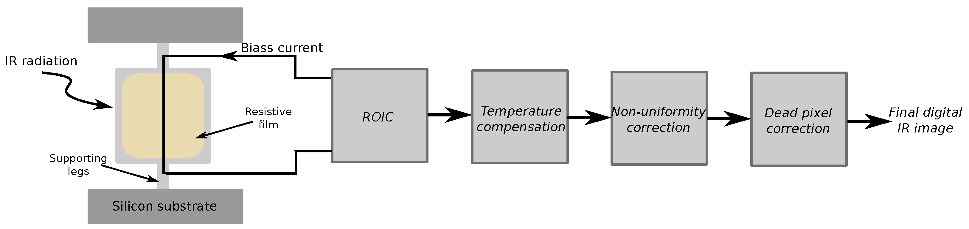
Article

Infrared Image Pre-Processing and IR/RGB Registration with FPGA Implementation

Institute of Electronics and Computer Science, 14 Dzerbenes St., LV-1006 Riga, Latvia
*
Author to whom correspondence should be addressed.
Electronics 2023, 12(4), 882; https://doi.org/10.3390/electronics12040882
Submission received: 18 January 2023 / Revised: 4 February 2023 / Accepted: 6 February 2023 / Published: 9 February 2023

Abstract

:
Infrared imaging sensors are frequently used in thermal signature detection applications in industrial, automotive, military and many other areas. However, advanced infrared detectors are generally associated with high costs and complexity. Infrared detectors usually necessitate a thermoelectric heater–cooler for temperature stabilization and various computationally complex preprocessing algorithms for fixed pattern noise (FPN) correction. In this paper, we leverage the benefits of uncooled focal plane arrays and describe a complete digital circuit design for Field Programmable Gate Array (FPGA)-based infrared image acquisition and pre-processing. The proposed design comprises temperature compensation, non-uniformity correction, defective pixel correction cores, spatial image transformation and registration with RGB images. When implemented on Xilinx Ultrascale+ FPGA, the system achieves a throughput of 30 frames per second using the Fraunhofer IMS Digital 17 μm QVGA-IRFPA with a microbolometer array size of 320 × 240 pixels and an RGB camera with a 1024 × 720 resolution. The maximum ratio of the standard deviation to the mean of 0.35% was achieved after FPN correction.

1. Introduction

Infrared (IR) imaging has been extensively used in a variety of different fields [1,2] and has undoubtedly solved visible spectrum imaging challenges. Advanced IR camera systems are frequently combined with visible light cameras to advantageously fuse the information from both sensors [2]. However, the downside of relying on infrared imaging has always been the high cost and complexity of the resulting system [3]. The correct operation of infrared detectors usually necessitates a thermoelectric heater–cooler for temperature stabilization, which contributes to the price and power consumption of the device. Additionally, IR sensors suffer from fixed pattern noise (FPN) caused by non-uniform responses of detectors. Likewise, ambient and internal temperature variations have an unequal effect on the characteristics of detectors. As a result, the processing unit in the camera system needs to perform several computationally complex correction tasks to recover meaningful information from the raw analog-to-digital converter (ADC) values [4].
To tackle these challenges, one approach is to leverage the benefits of microbolometer focal plane arrays (FPA), which have the advantage over photon detectors to operate without cooling [5]. Over the past two decades, continuous advancements in CMOS/MEMS photolithography have been sufficient for fabricating small-pixel microbolometer detectors [6]. The combination of manufacturing processes and uncooled detector designs has allowed significant performance and yield improvements. Hence, commercially manufacturing high-volume, low-cost and high-operation temperature infrared sensors has become possible. Removing unnecessary thermoelectric parts, in effect, improves reliability and power efficiency and reduces cost, which is crucial in low-cost or power-critical applications where reduced complexity of packaging is decisive.
Although infrared bolometer thermal effects and their respective correction algorithms have been widely studied [7,8,9] and simulated [10], efficient implementation without introducing a significant delay is critical in real-time applications. In this work, we propose implementing computationally intensive algorithms in a register transfer level (RTL) for field programmable gate array (FPGA)-based uncooled IR imaging system. The proposed approach adopts pipelining design technique and reduces data processing delay for every frame, while ensuring real-time acquisition and thermal effect correction. The presented work follows a research initiative for exploring potential solutions to reduce the costs of IR imaging. The developed prototype is a step towards a potential (processorless) IR camera with low-latency processing suitable for safety-critical applications.

2. Thermal Effect Overview

Resistive microbolometers are a type of radiation temperature sensor that operates at ambient temperature. They are fabricated as thin resistive film microbridges suspended over a cavity in a silicon substrate and encapsulated in a vacuum to improve thermal isolation. The incident IR radiant flux is absorbed by the detector element and converted into an electrical signal [11]. Figure 1 represents a single detector and the measuring chain. Although the heat exchange with the residual surrounding gas is low, unavoidable thermal conduction still occurs through the supporting legs. Unwanted temperature fluctuations of the silicon substrate affect the thin film due to thermal conductance, and imbalanced tolerances of the bolometers produce a non-uniform response to IR radiation. Lastly, manufacturing defects cause unresponsive pixels throughout the imaging sensor. Various methods have been explored to mitigate these effects, which we summarize in the following chapters.

2.1. Sensor Temperature

Commercial uncooled infrared sensors most commonly utilize resistive microbolometers for radiation detection [5]. The microbolometer absorbs infrared radiation and converts it into heat, which changes the temperature-dependent resistance of the thermistor material. The temperature corresponds to the measurements of the resulting resistance change. Microbolometer array-based infrared sensors typically have a read-out integrated circuit (ROIC) to measure the signal on each detector.
In the readout circuit, an integrating amplifier measures the current flowing through an active bolometer, which depends on the detector’s self-temperature. The temperature of the microbolometer detector used in the thermal camera correlates with the temperature of the observed object in the scene; nonetheless, it is also influenced by internal sources, i.e., camera body or detector substrate. To reduce the heat exchange with the surrounding gaseous environment, the detector array is encased in a sealed wafer-level vacuum cavity. Furthermore, each bolometer is suspended and thermally isolated on relatively long legs with a small cross-sectional area to achieve good thermal insulation from the supporting substrate [12].
Despite this, due to the limitations of the lithography tools available to manufacture suspended structures, the thermal conductance of the legs is presently much larger than the radiation conductance, especially for smaller pixels [13]. To compensate for the remaining influence of the detector’s self-temperature, the signal is usually compensated using a blind reference bolometer, which has a reduced responsivity to the incident infrared radiation [14]. Generally, this compensation may occur digitally after the bolometer readout or, alternatively, can be performed by the readout circuitry itself.

2.2. Sensor Non-Uniformity

Raw infrared sensor image data are known to be highly non-uniform due to the varying sensitivity of the individual elements caused by the manufacturing process mismatches. Although non-uniformity is present in all image sensors, it is especially noticeable in infrared due to the low contrast of the scene [15]. Readout circuits may have a shared amplifier for each row or column of the imager. Variations of their parameters alongside self-temperature compensation may cause image noise with a striped pattern. A combination of both artefacts is commonly referred to as a fixed pattern or spatial noise. In addition, the sensitivity and other parameters change based on the sensor temperature; therefore, the noise pattern changes during the camera operation. This effect is known as temporal or temperature-dependent noise.
Several methods for non-uniformity correction (NUC) have been developed. Calibration-based or reference-based NUC requires characterization of the sensor non-uniformity. It is conducted by pointing the camera at uniform scenes with known temperatures and calculating the coefficients to correct the noise in the perceived image. Two-point correction is the one used most commonly. It requires measurements at two different temperatures and produces a set of gain and offset coefficients for each image pixel. Piecewise linear correction is another method used when higher precision is necessary [7]. Calibration-based NUC has a simple implementation and requires little non-volatile storage space to store the calibration coefficients. The major downside, however, is the necessity to perform the calibration procedure in the factory and the sensor’s parameter degradation.
The result of the fixed pattern noise correction is only valid at a specific sensor temperature where non-uniformity was characterized; therefore, in the case of uncooled sensor designs, one must consider temperature variation. Nugent et al. [8] propose using two sets of gain and offset coefficients for each pixel, both dependent and independent of the sensor temperature; therefore, both spatial and temporal corrections are performed simultaneously. Lin et al. [9] performed the temporal NUC in two stages. First, the influence of the FPA’s temperature is described with a set of second-order polynomials. To account for the errors due to the temperature instability, third-order polynomials are used to describe the influence of the temperature’s rate of change. Only after these adjustments, the spatial NUC eliminates the fixed pattern noise. Budzier and Gerlach [16] perform the temporal correction after spatial; thus, the temperature influence is an offset described by a third-order polynomial.
As an alternative to the calibration-based methods, several scene-based methods exist. Instead of relying on precise information about the camera sensor, these methods operate based on assumptions about the observed scene. As such, they do not require factory calibration or drift compensation. The natural downside of these methods is the increased computational complexity and storage demands. They also require a certain amount of motion, i.e., in the scene or camera movement itself. Scene-based methods can be subdivided into statistical, registration and neural network-based methods.
The calibration approach will be the preferred method in this article to achieve a good balance between implementation cost and detector response equalization performance. The two-point correction will be conducted performing the calibration procedure beforehand. The reconfigurable SoC FPGA platform lends itself to other methods as well at the cost of a higher logic and memory utilization.

2.3. Defective Pixels

It is common for imaging sensors to have several defective pixels with such an abnormal level of sensitivity that their value does not provide any information about the observed scene. The fraction of such defects in sensors that pass the manufacturer’s quality assurance procedures usually does not exceed several percent of the total pixel amount, and they are spread evenly across the sensor; thus, their presence manifests as impulse noise superimposed on the image. Visible noise degrades the perceived quality of the image and may interfere with certain processing operations; therefore, noise mitigation techniques must be employed. The median filter is well known for effectively suppressing impulse noise. However, due to its space invariance, applying it to the whole image results in a loss of fine details, especially with larger window sizes. Adaptive or switching filters were introduced as a solution to this problem. Switching filters essentially consist of fault detection and correction blocks, thus ensuring that filtering occurs only when the detected noise surpasses a certain threshold [17].
Pixel defects in literature are structured into two broad categories: salt-and-pepper noise or catastrophic faults, where defective pixels are either dark or at full brightness, and random valued noise or parametric faults, where pixels may have any brightness. Salt-and-pepper noise is much easier to detect. In fact, some simple algorithms operate on the assumption that pixels with maximum or minimum values are most likely defective. Many defective pixel detection algorithms employing various radiometric calibration methods for measuring detector response have been described in the literature [18,19,20]. In this work, the nature of defects and detection of unresponsive pixels inside the processing chain is not of concern since we will use a calibration map provided during the calibration process. A technique related to the adaptive methods will be used to selectively reconstruct values from adjacent bolometers.

3. Related Work

In [21], the image processing and FPA control module consists of an FPGA and a microcontroller. The FPGA performs all real-time image processing tasks, generates the sensor control signals and includes a VGA controller for video output. The microcontroller is responsible for temperature measurements, supervision of the image processing operations and parameter calculations for non-uniformity correction. To ensure proper operation of the unstabilized FPA over a broad temperature range, the microcontroller also controls the microbolometer supply voltages that determine the sensitivity of the detectors and the level of the output signal. The software was written in the C programming language with assembler routines for time-sensitive calculations. Overall, the work is a good example of a two-chip FPA controller architecture, but the advent of modern SoC FPGAs facilitates a more compact single-chip solution. The nearest neighbor defective pixel filtering could also be conducted more accurately with other relatively simple methods, such as bilinear interpolation.
Bieszczad [22] describes the Soc FPGA implementation of an infrared polarimetric teledetection system. The imaging system consists of two detector arrays with continuously rotating polarizers. It performs data fusion in software with frame rates ranging from 12 to 46 frames per second, depending on the image processing options. One of the most computationally expensive operations managed by the software is geometric transformation and co-registration of two separate channels. We improve upon this topic in our proposed architecture by migrating spatial image transformation to hardware.
Forsberg et al. [12] developed an evaluation camera module based on Altera Cyclone III FPGA. The module was assembled from three custom-printed circuit boards with a socket for an uncooled microbolometer focal plane array. The FPGA provides high computing power to implement camera control and image processing algorithms. The authors describe the full wafer-level design process for microbolometer arrays and report on operational infrared focal plane arrays utilizing mono-crystalline Si/SiGe quantum-well microbolometers that are heterogeneously integrated on top of CMOS-based read-out integrated circuit substrates. Although the work demonstrates the attainability of an uncooled microbolometer detector-based camera module, further details on image processing and compensation for thermal effects are not specified.
In this work, we embrace the trend of heterogeneous integration for uncooled FPA processors. Besides the usual fixed pattern and thermal effect correction algorithms, we extend upon the capabilities of infrared and visible image component co-registration.

4. Digital Circuit Design

Creating a dedicated infrared FPA preprocessing circuit involves designing a system incorporating several image-processing algorithms and compensating for the different thermal effects. The approach in this work is to exploit the heterogeneous systems-on-chip (HSoC) FPGA architecture by implementing all of the computationally intensive tasks in digital logic and using the microprocessor unit (MPU) for orchestrating data movement to/from FPGA-based accelerators. Notably, before the deployment on a physical system, IR preprocessing algorithm designs were validated using functional simulations and synthetic data [10].

4.1. Overall System Architecture

In the overall image processing architecture represented in Figure 2, two parallel AXI-Stream compliant pipelines are implemented for infrared and RGB image processing.
AXI Memory-Mapped to AXI-Stream direct memory access (DMA) controllers transfer images and calibration coefficients from the system memory. Temperature compensation, Non-Uniformity Correction, Defective Pixel Correction and Spatial Image Transformation reside in the first stream, whilst the second stream is responsible for RGB image transformation. The Registration block is necessary to synchronize rectified images from the two streams and place them onto a common coordinate system to enable data enhancement in later processing stages. Bypass data paths permit separate evaluations of every correction algorithm. Each of the custom modules implemented in programmable logic (PL) is configured from the hard processing system (PS), which also initiates data transfers from the shared system memory. The user application running in the Linux operating system uses TCP/IP over Gigabit Ethernet to send the final processed digital image to the visualization application on a host system.
A custom IR Camera Driver interfaces with the QVGA IR Camera to read the raw pixel values and transfer the data to the Memory-Mapped interface. The captured frames are buffered in the system memory since the QVGA IR Camera used in this work operates in a continuous acquisition mode. In this way, the necessity for a large FIFO and the risk of overflowing the FIFO is avoided.

4.2. Temperature Compensation

Temperature compensation utilizes shaded pixels to interpolate temperature-dependent bolometer values for each of the pixels and subtracts them from the illuminated bolometer ADC values. Figure 3 depicts the temperature dependency correction architecture utilized in this work.
We correct the active microbolometers using the shaded microbolometers in the same row. The chosen sensor has ten shaded bolometers on each side. We store and compute the average values P ¯ L e f t and P ¯ R i g h t for shaded microbolometers from the beginning and end of the row, respectively. We use these averaged values to define a straight-line function S ( w ) vs. the pixel location in the row:
S ( w ) = P ¯ L e f t ( 1 w ) + P ¯ R i g h t w .
Here, w is a weight factor defined by the distance between the first column and the pixel location:
w ( x ) = x x 0 N ,
where x is the location of the pixel in the row, x 0 is the number of the first column of active pixels and N is the number of active pixels. Then, the temperature-compensated value P x y is computed:
P x y = P x y S ( w ) .
Further, we compute the mean values with running average over subsequent frames and make the averaging parameter adjustable (small for high-pass filter, large for low-pass filter) and use these “running”/”filtered” mean values for determining the straight line.

4.3. Non-Uniformity Correction

The infrared image processing pipeline includes a basic two-point non-uniformity correction block shown in Figure 4.
A calibration procedure is applied to find offset and gain coefficients for every raw pixel. The gain and offset coefficients are applied accordingly to the response of the sensor P x y to find the non-uniformity corrected value P x y at the ( x , y ) coordinates:
P x y = G x y P x y + O x y .
where O x y is the offset coefficient and G x y is the gain coefficient.
Raw pixel values and the coefficients are delivered to the processing unit from the system memory using AXI Memory-Mapped to the AXI-Stream DMA engine. Since data alignment between the streams is not guaranteed, an AXI-Stream synchronizer adjusts simultaneous throttling for all data streams. Apparently, the implementation of a simple two-point algorithm requires only a small amount of logic blocks and memory resources for only two coefficients per pixel. It can be considered a reasonable solution for real-time applications requiring a low hardware footprint.

4.4. Defective Pixel Correction

Defective pixel replacement, as shown in Figure 5, is based on interpolation using the nearest pixels surrounding the defective pixel. It is a fully pipelined-switched interpolator design capable of arranging data in a moving window and performing bilinear interpolation. The component selectively interpolates only at the coordinates of defective pixels. The defective pixels are identified beforehand at the FPA calibration stage and corresponding coordinates are stored in the memory.
Because of the low amount and sparsely located defective pixels, the pixel coordinates can be transferred over the Memory-Mapped interface beforehand and stored as array constants in Block Memory or Look-Up Tables. The validity information can be further converted into a 1-bit wide AXI-stream. Both streams are synchronized before the dead pixel correction stage receives them.
A 3 × 3 sliding window accumulates the nearest eight neighbors N 8 ( P x y ) around the potentially defective pixel P x y . Four diagonal neighbors N d ( P x y ) are further used for bilinear interpolation i n t e r p ( N d ( P x y ) ) , which is chosen due to its arithmetic simplicity. The bilinear interpolation core then estimates the intensity value P x y at the given defective pixel location ( x , y ) . A normalized weighting bilinear interpolation scheme (Figure 6) consisting of three linear interpolations can be used. The pixels on the vertices of a unit square ( P 1 , P 2 , P 3 , P 4 ) construct a new data value inside the square. Assuming the values change linearly between the vertices, we can perform two linear interpolations in the x direction:
R 1 = P 1 ( 1 w x ) + P 2 w x
R 2 = P 3 ( 1 w x ) + P 4 w x .
We then interpolate between those interpolated values R 1 , R 2 in the y direction to get the result P:
P = R 1 ( 1 w y ) + R 2 w y ,
where w x and w y are the normalized weight factors, which determine the influence of each neighboring pixel. In this case, the interpolant always resides in the center of the quadrilateral and the weights are equal w x = w y = 0.5 .
The candidate pixel is replaced with the interpolation result if the according defective pixel map bit B x y is set. Otherwise, the original pixel value is delayed, and the preserved value is used as the output. Edge pixels are handled by extending the nearest available pixel values. The edge pixel remapping stage checks the current location of the pixel and decides whether rearranging the convolution matrix due to edge proximity is necessary.

4.5. Spatial Image Transformation

The spatial image transformation core, as such, is a sophisticated image processing design, and its detailed description is beyond the scope of this work. Instead, we guide the reader to [23] and here give a brief overview. Figure 7 illustrates the architecture of the spatial image transformation component.
It consists of Read and Write Masters, Dual-Port Memory Matrix, Inverse Transformation Computing logic, Demultiplexing logic and a Reconstruction block. The spatial transformation accelerator’s working principle relies on the sequential estimation of the consecutive output sample’s location in the input image and reconstructing it using buffered input samples. The solution necessitates computing the inverse transformation and retrieving the corresponding input coordinate pair for the consecutive output coordinates:
( x i n , y i n ) = f 1 ( x o u t , y o u t ) .
where x i n , y i n and x o u t , y o u t are the input/output image coordinates, and f is some arbitrary function, expressed as a matrix operator for linear transformations.
Output coordinates for the Inverse Transformation Computation are provided by the Memory Read-Write master. This structure enables simultaneously writing input data to memories and calculating the appropriate read addresses for the output data. Each output pixel can be reconstructed using adjacent pixels in the input image. Dual Port Memory Matrix and Memory Write-Read Masters retrieves the necessary neighboring pixels from the memories. The Demultiplexing logic arranges read pixel data for the Reconstruction, e.g., bilinear or bicubic interpolation. For higher-quality approximation results, we implement bicubic interpolation, which involves retrieving sixteen nearest neighbors and utilizing sixteen buffers in the memory matrix accordingly.
Memory-Mapped interface ensures configuration of the Inverse Transformation Computing logic. A Matrix Multiplication core calculates the inverse transformation for any arbitrary linear image transformation, such as translation and rotation. This core also provides the image rectification ability to project IR and RGB images onto a common image plane. Other custom coordinate processors can be used just as well, for example, a processor for calculating a lens distortion correction transformation. In the current configuration, Matrix Multiplication is cascaded with a Lens Distortion Correction instance. To correct radially distorted images, we follow the digital circuit architecture for calculating the Barrel distortion correction transformation defined in [24].

5. Results

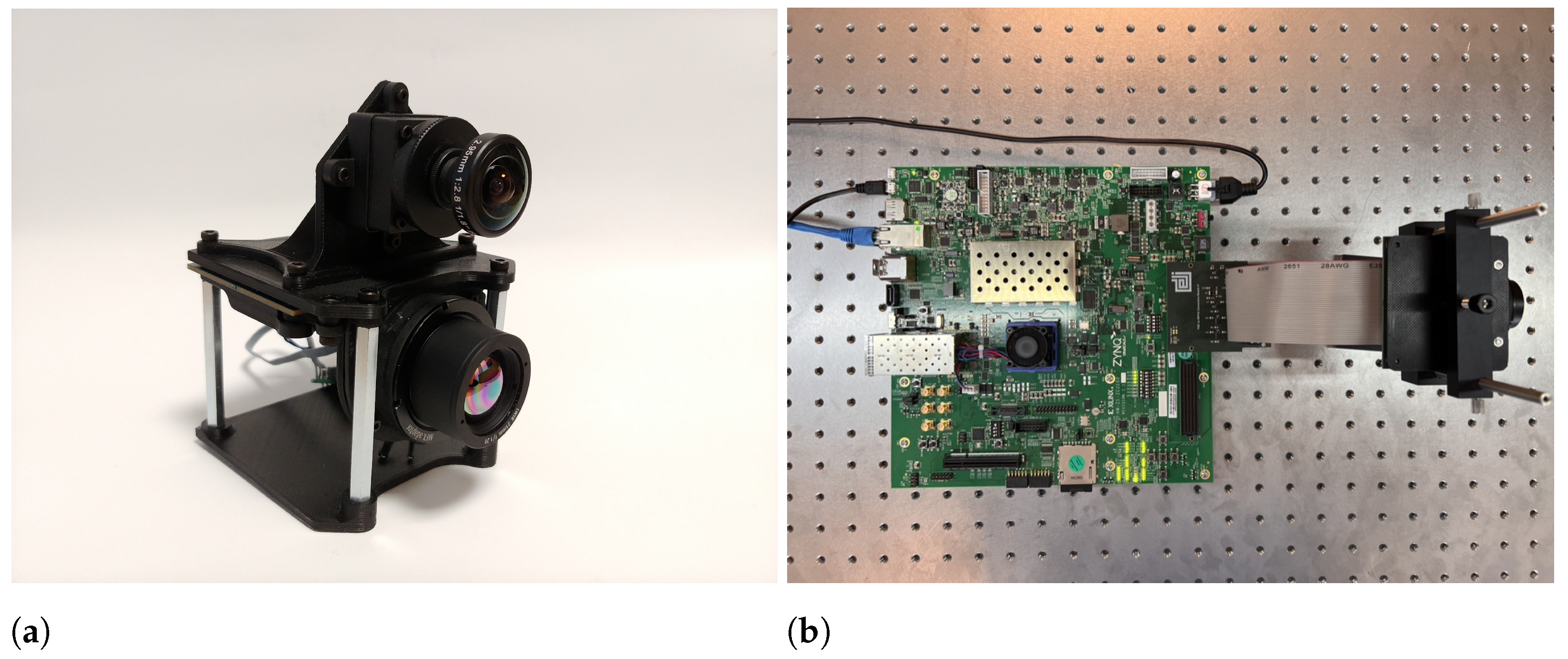
The experimental setup depicted in Figure 8 consists of a combined IR and RGB camera fixture (Figure 8a) and an electronics evaluation board (Figure 8b). A Xilinx ZCU102 Evaluation platform was used to implement the system on a Xilinx Ultrascale+ XCZU9EG FPGA. The system was coded using VHDL and synthesized for the target SoC. Fraunhofer IMS infrared bolometer focal plane array Digital 17 μm QVGA-IRFPA [25] with an array of 320 × 240 microbolometer pixels and a pixel pitch of 17 μm × 17 μm constituted the infrared pixel source. 
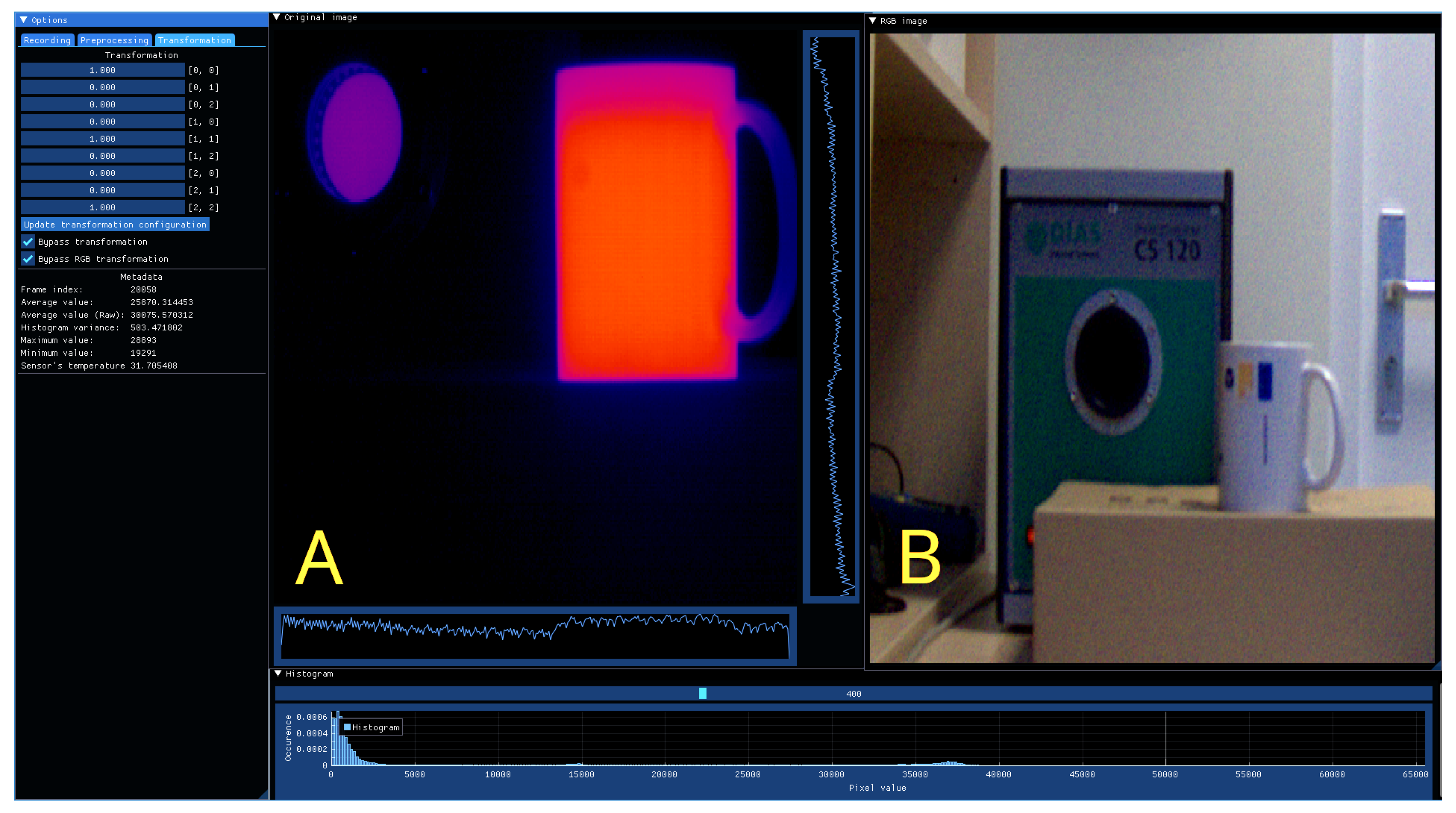
Figure 9 illustrates the control and visualization application residing on a host PC. General controls and configuration of image transformation IP core are implemented in the modular Dear ImGui GUI building framework [26].
Table 1 shows the resource utilization of the digital logic design. A complete system utilizes 445 hardware multipliers, 57,474 logic cells, 79,894 registers and 171 BRAM blocks. The high block RAM unit count is associated with pixel buffering in the spatial image transformation core, and the lens distortion correction requires a considerable amount of buffered samples. In the case of highly distorted images, the inverse distortion correction transformation calculates sparse read address inquiries. Hence, sizable internal memory is required. Interpolation cores in the defective pixel correction and both transformation cores and the inverse transformation compute logic contribute to the high usage of DSP units. Spatial image transformation resources are represented separately as “Transformation” and “Undistortion” measurements to distinguish the amount of logic added by the lens distortion correction unit.
Furthermore, the FPGA easily accommodates the design and supports the maximum clock frequency of 99 MHz. The data transfer rates between the custom RTL design unit and hard processing system are sufficient to ensure the 320 × 240 IR and 1024 × 720 RGB image transfer rate of 30 frames per second, which is the maximum operating speed of the infrared camera.
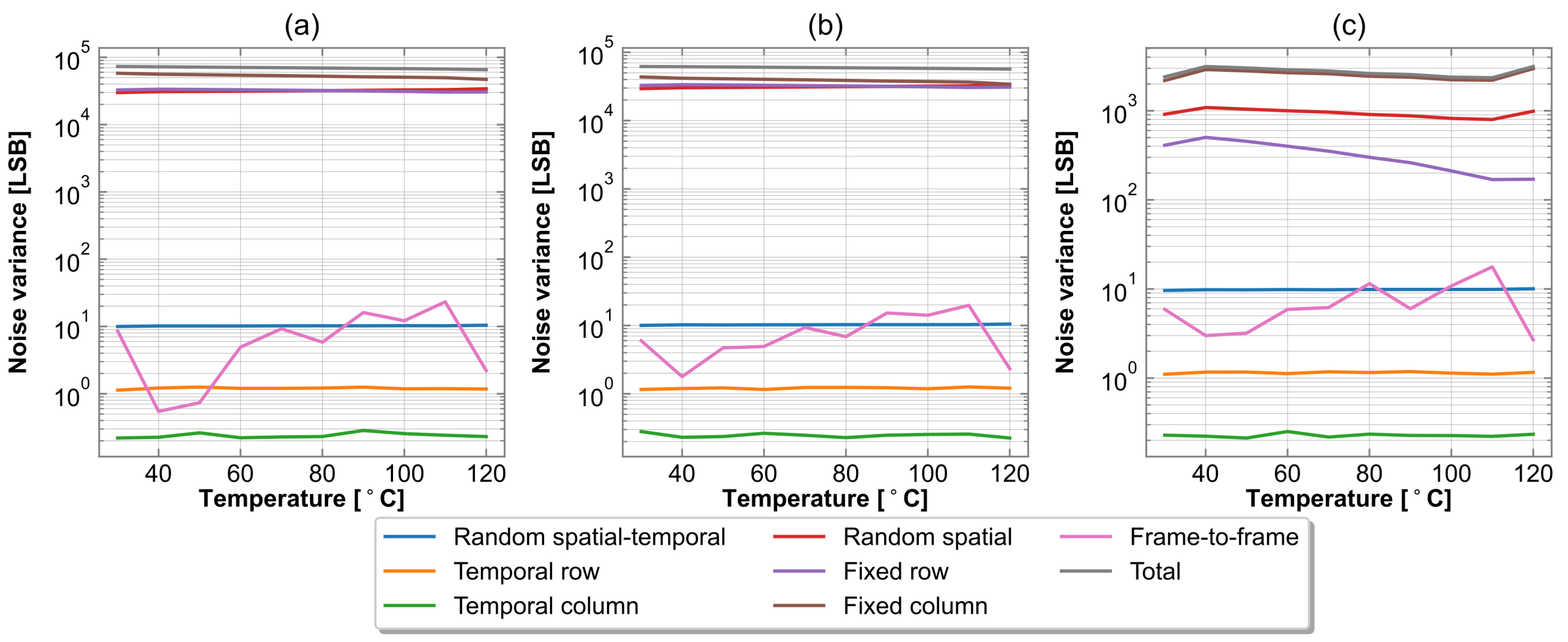
To fully characterize the FPA and the effectiveness of the thermal effect correction algorithms, the 3D-Noise methodology is required [27]. The method takes a sequence of t frames with horizontal width h and vertical height v and extracts seven orthogonal noise components. Noise components may be static or temporally varying. The noise component measurements are made using a series of directional averaging operators, which extract each noise type and remove that component from the original 3D array. The total measured cube consists of the mean value of the cube and all of the separate noise components:
U ( t , v , h ) = U ¯ ( t , v , h ) + N t ( t ) + N v ( v ) + N h ( h ) + N t v ( t , v ) + N t h ( t , h ) + + N v h ( v , h ) + N t v h ( t , v , h )
where U ¯ ( t , v , h ) is the mean value of the cube, N v h , N v , N h are temporally correlated spatial noise components, N t , N t v , N t h are spatially correlated temporal noise components and N t v h is the random spatio-temporal noise. Since the noise components are uncorrelated and independent, the sum of squared variances can be used to estimate the resultant noise variance.
A sequence of 100 frames was acquired while the camera pointed toward a uniform blackbody scene. The temperature of the blackbody was adjusted in the range of 30 ° C to 120 ° C . The 3D-Noise algorithm was applied to extract the noise components from the image array and calculate corresponding variances. The measurement series were repeated, while consecutively enabling correction IPs. In the final experiment, all components were enabled at once.
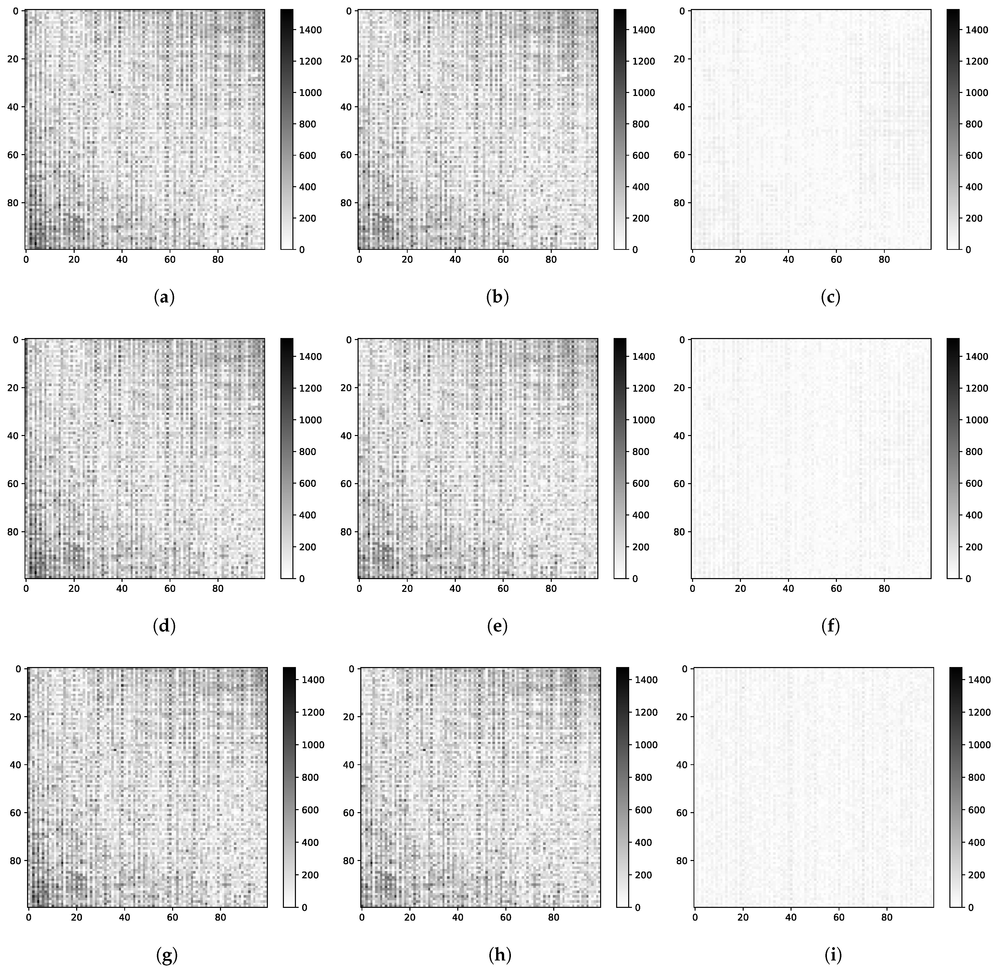
Figure 10 shows the side-by-side comparison of the variance of the noise components after each of the correction steps. As a baseline, the noise components without any corrections are given in Figure 10a. The temporally varying noise is visually indistinguishable due to the tendency of the eye to integrate the noise over time; nonetheless, the 3D-Noise analysis reveals that this noise is present. The random spatio-temporal noise N t v h is close to equivalent to thermal resolution defined by noise equivalent temperature difference (NETD). It remains consistent throughout the measurement range reaching the maximum variance of σ t v h 2 = 10.43 LSB at 120 ° C . Regardless, the major contribution to the overall noise is the spatially-varying noise components.
The mean value of the image was calculated and used to find the absolute difference error to emphasise the deviation from the uniform average value:
A E v h = | U ¯ ( t , v , h ) U ¯ v h ( t , v , h ) | ,
where U ¯ v h ( t , v , h ) is the time-averaged signal in the VH-plane. Results in Figure 11 show absolute difference errors in images from the 3D-Noise measurement series before and after each of the corrections at 30 ° C , 70 ° C and 120 ° C . As can be seen from Figure 11a,b,d, before the correction is applied, variability in pixel sensitivity is clearly visible, especially the fixed pattern noise among the columns. In fact, noise measurements in Figure 10a confirm that the majority of total noise comes from non-uniform sensitivity in columns. In Figure 11a, spatial column variance is σ h 2 = 58,015.6 LSB from the total variance of σ T o t a l 2 = 73,051.5 LSB, whereas the spatial row variance is only σ v 2 = 32,769.6 LSB.
Figure 11b,e,h depict the infrared image after fixed pattern noise caused by internal temperature variations has been compensated. Variance measurements of spatial noise components reveal that the compensation evenly reduces row, column and random spatial noise components over the measured temperature interval, producing a slightly lower reduction from the total variance of σ T o t a l 2 = 65,609.3 LSB to σ T o t a l 2 = 56,750.8 LSB at 120 ° C . Even so, the spatially-varying noise due to uneven detector responsivity remains predominant.
Figure 11c,f,i show the effect of applying the non-uniformity correction. The total variance decreases substantially to σ T o t a l 2 = 2401.1 LSB at 30 ° C . The column noise with variance σ h 2 = 2182.1 LSB is still dominant in this case, although it is much less noticeable. Figure 10c illustrates that the spatial noise levels are mostly reduced in the entire input signal range, while in some measurement intervals, the two-point correction algorithm is not equally effective. At 120 ° C , the combined correction algorithms perform the worst, reaching the total noise variance of σ T o t a l 2 = 3137.1 LSB. Computing the maximum ratio of standard deviation to the mean at this point reveals that a 0.35% level of non-uniformity was achieved after FPN correction.
Figure 12a shows a closer inspection of the image captured from the camera while looking at a thermally uniform source. The region includes two defective pixels, which are clearly visible after temperature compensation and non-uniformity correction. The image captured after defective pixel correction is shown Figure 12b and indicates bilinear interpolation successfully eliminating unresponsive pixels.
As far as we know, this is the only published work encompassing noise correction, geometric transformation, lens distortion correction and image registration in a single FPGA system. Thus, to compare our implementation to other work, we look at closely related solutions, including either one of the processing components. Our implementation in different configurations and existing solutions are summarized in Table 2. As can be seen, our system with camera control logic, temperature compensation and FPN correction requires more resources than similarly equipped infrared FPA processors. Adding perspective transformation and image undistortion allows observing the impact of these components on the design implementation in comparison to IR/RGB registration in [28] and lens distortion correction in [29]. Despite this, the increased size and power of the system are justified since the coordinate transformations are calculated on-the-fly and arbitrary geometric transformations are performed in the programmable logic domain.
The spatial image transformation core is thoroughly evaluated by Novickis et al. [23] with various practical image manipulations. Contrary to [21,28], the module allows mapping one image onto another directly in hardware, while maintaining the native frame rate of the IR camera.

6. Conclusions

The article describes a complete digital circuit design for SoC FPGA-based infrared image acquisition and processing. The system supports data acquisition from a 320 × 240 infrared image sensor and integrates temperature compensation, non-uniformity correction, dead pixel correction cores and spatial image transformation IP cores. The thermal effect pre-processing components ensure correction for different effects related to the infrared bolometer array, whereas the spatial transformation can perform arbitrary geometric transformations. The system encompasses a second image processing branch for images from a 1024 × 720 RGB camera. Data from both cameras are projected onto a common plane utilizing the transformation core and are afterwards used to augment the IR image. The system was implemented on a Xilinx Ultrascale+ XCZU9EG SoC and achieves a maximum throughput of 30 frames per second.
The image processing quality was evaluated using the 3D-Noise method, which separates individual spatial and temporal noise components. Data cubes were captured at different blackbody temperatures to observe any temperature dependence. In the case of the particular system, the spatially-varying noise component was identified as the most significant contribution to the overall noise. The ratio of noise standard deviation to the mean revealed that, at most, a 0.35% level of non-uniformity remains after all FPN correction procedures.
Compared to similar infrared image pre-processing and registration architectures, our work embeds the projective transformation capability directly in the hardware. As such, the system reduces the frame rate restrictions encountered elsewhere. For future research, we intend to employ the proposed system as a low-cost mixed-mode visible and thermal imaging system to produce enhanced infrared images. We plan to use the resulting data with custom perception algorithms for improved object detection.

Author Contributions

Conceptualization, R.N.; funding acquisition, K.O.; investigation, E.L.; methodology, R.N.; project administration, K.O.; software, R.N.; supervision, R.N.; validation, E.L.; visualization, E.L.; writing—original draft, E.L. and A.C.; writing—review and editing, R.N. All authors have read and agreed to the published version of the manuscript.

Funding

This work is the result of activities within the APPLAUSE project, which has received funding from ECSEL Joint Undertaking (JU) under grant agreement No. 826588. The JU receives support from the European Union’s Horizon 2020 research and innovation program and Belgium, Germany, Netherlands, Finland, Austria, France, Hungary, Latvia, Norway, Switzerland, Israel.

Data Availability Statement

The data presented in this study are available on request from the corresponding author.

Conflicts of Interest

The authors declare no conflict of interest.

References

  1. Kylili, A.; Fokaides, P.; Christou, P.; Kalogirou, S. Infrared thermography (IRT) applications for building diagnostics: A review. Appl. Energy 2014, 134, 531–549. [Google Scholar] [CrossRef]
  2. Deng, Q.; Tian, W.; Huang, Y.; Xiong, L.; Bi, X. Pedestrian Detection by Fusion of RGB and Infrared Images in Low-Light Environment. In Proceedings of the 2021 IEEE 24th International Conference on Information Fusion (FUSION), Sun City, South Africa, 1–4 November 2021; pp. 1–8. [Google Scholar] [CrossRef]
  3. Roxhed, N.; Niklaus, F.; Fischer, A.; Forsberg, F.; Höglund, L.; Ericsson, P.; Samel, B.; Elfving, A.; Simonsen, T.; Wang, K.; et al. Low-Cost Uncooled Microbolometers for Thermal Imaging. In Optical Sensing and Detection; SPIE: Bellingham, WA, USA, 2010; Volume 7726. [Google Scholar] [CrossRef]
  4. Cao, Y.; He, Z.; Yang, J.; Ye, X.; Cao, Y. A multi-scale non-uniformity correction method based on wavelet decomposition and guided filtering for uncooled long wave infrared camera. Signal Process. Image Commun. 2018, 60, 13–21. [Google Scholar]
  5. Kruse, P. Can the 300-K radiating background noise limit be attained by uncooled thermal imagers? In Infrared Technology and Applications XXX; SPIE: Bellingham, WA, USA, 2004; Volume 5406. [Google Scholar] [CrossRef]
  6. Yu, L.; Guo, Y.; Zhu, H.; Luo, M.; Han, P.; Ji, X. Low-Cost Microbolometer Type Infrared Detectors. Micromachines 2020, 11, 800. [Google Scholar] [CrossRef] [PubMed]
  7. Milton, A.F.; Barone, F.R.; Kruer, M.R. Influence Of Nonuniformity On Infrared Focal Plane Array Performance. Opt. Eng. 1985, 24, 855–862. [Google Scholar]
  8. Nugent, P.W.; Shaw, J.A.; Pust, N.J. Correcting for focal-plane-array temperature dependence in microbolometer infrared cameras lacking thermal stabilization. Opt. Eng. 2013, 52, 061304. [Google Scholar] [CrossRef]
  9. Lin, D.; Maas, H.G.; Westfeld, P.; Budzier, H.; Gerlach, G. An advanced radiometric calibration approach for uncooled thermal cameras. Photogramm. Rec. 2017, 33, 30–48. [Google Scholar] [CrossRef]
  10. Leja, L.; Purlans, V.; Novickis, R.; Cvetkovs, A.; Ozols, K. Mathematical Model and Synthetic Data Generation for Infra-Red Sensors. Sensors 2022, 22, 9458. [Google Scholar] [CrossRef] [PubMed]
  11. Budzier, H.; Gerlach, G. Thermal Infrared Sensors. In Thermal Infrared Sensors; John Wiley & Sons, Ltd.: Hoboken, NJ, USA, 2011; Chapter 6; pp. 149–251. [Google Scholar] [CrossRef]
  12. Forsberg, F.; Lapadatu, A.; Kittilsland, G.; Martinsen, S.; Roxhed, N.; Fischer, A.C.; Stemme, G.; Samel, B.; Ericsson, P.; Høivik, N.; et al. CMOS-Integrated Si/SiGe Quantum-Well Infrared Microbolometer Focal Plane Arrays Manufactured with Very Large-Scale Heterogeneous 3-D Integration. IEEE J. Sel. Top. Quantum Electron. 2015, 21, 30–40. [Google Scholar] [CrossRef] [Green Version]
  13. Lohrmann, D.J.; Littleton, R.T.; Reese, C.E.; Murphy, D.F.; Vizgaitis, J.N. Uncooled long-wave infrared small pixel focal plane array and system challenges. Opt. Eng. 2013, 52, 061305. [Google Scholar]
  14. Haider, S.; Majzoub, S.; Alturaigi, M.; Abdelrahman, M. Pair-Wise Serial ROIC for Uncooled Microbolometer Array. IEIE Trans. Smart Process. Comput. 2015, 4, 251–257. [Google Scholar] [CrossRef]
  15. Lloyd, J.M. Thermal Imaging Systems; Plenum Press: New York, NY, USA, 1975; pp. 275–282. [Google Scholar]
  16. Budzier, H.; Gerlach, G. Calibration of uncooled thermal infrared cameras. J. Sens. Sens. Syst. 2015, 4, 187–197. [Google Scholar]
  17. Bernstein, R. Adaptive nonlinear filters for simultaneous removal of different kinds of noise in images. IEEE Trans. Circuits Syst. 1987, 34, 1275–1291. [Google Scholar] [CrossRef]
  18. Chan, C.H. Dead Pixel Real-Time Detection Method for Image. U.S. Patent 7,589,770 B2, 15 September 2009. [Google Scholar]
  19. Chen, C.; Cho, C.; Sun, Y.; Chen, T.; Su, C. Low complexity photo sensor dead pixel detection algorithm. In Proceedings of the 2012 IEEE Asia Pacific Conference on Circuits and Systems, Kaohsiung, Taiwan, 2–5 December 2012; pp. 360–363. [Google Scholar]
  20. Tchendjou, G.T.; Simeu, E. Detection, Location and Concealment of Defective Pixels in Image Sensors. IEEE Trans. Emerg. Top. Comput. 2020, 9, 664–679. [Google Scholar]
  21. Sosnowski, T.; Bieszczad, G.; Kastek, M.; Madura, H. Processing of the image from infrared focal plane array using FPGA-based system. In Proceedings of the 17th International Conference Mixed Design of Integrated Circuits and Systems—MIXDES 2010, Wroclaw, Poland, 24–26 June 2010; pp. 581–586. [Google Scholar]
  22. Bieszczad, G. SoC-FPGA embedded system for real-time thermal image processing. In Proceedings of the 2016 MIXDES—23rd International Conference Mixed Design of Integrated Circuits and Systems, Lodz, Poland, 23–25 June 2016; pp. 469–473. [Google Scholar] [CrossRef]
  23. Novickis, R.; Lielāmurs, E.; Justs, D.J.; Cvetkovs, A.; Ozols, K. Spatial Transformation Accelerator with Parallel Data Access Scheme for Sample Reconstruction. Image Process. J. 2023; Submitted. [Google Scholar]
  24. Novickis, R. Implementation of Stereo-Vision Algorithms in Heterogeneous Embedded Systems. Ph.D. Thesis, Riga Technical University, Riga, Latvia, 2020. [Google Scholar]
  25. Digital 17 μm IRFPA. Available online: https://www.ims.fraunhofer.de/en/Business_Units_and_Core_Competencies/IR-Imagers/Technologies/Digital-IRFPA.html (accessed on 4 February 2023).
  26. Dear ImGui. Available online: https://github.com/ocornut/imgui (accessed on 4 February 2023).
  27. O’Shea, P.D.; Sousk, S.F. Practical issues with 3D noise measurements and application to modern infrared sensors. In Infrared Imaging Systems: Design, Analysis, Modeling, and Testing XVI; SPIE: Bellingham, WA, USA, 2005. [Google Scholar]
  28. Inostroza, F.; Díaz, S.; Cárdenas, J.; Godoy, S.E.; Figueroa, M. Embedded registration of visible and infrared images in real time for noninvasive skin cancer screening. Microprocess. Microsystems 2017, 55, 70–81. [Google Scholar] [CrossRef]
  29. Clapa, J.; Blasinski, H.; Grabowski, K.; Sekalski, P. A fisheye distortion correction algorithm optimized for hardware implementations. In Proceedings of the 2014 21st International Conference Mixed Design of Integrated Circuits and Systems (MIXDES), Lublin, Poland, 19–21 June 2014. [Google Scholar] [CrossRef]
  30. Redlich, R.; Figueroa, M.; Torres, S.N.; Pezoa, J.E. Embedded nonuniformity correction in infrared focal plane arrays using the Constant Range algorithm. Infrared Phys. Technol. 2015, 69, 164–173. [Google Scholar]
  31. Njuguna, J.C.; Alabay, E.; Çelebi, A.; Çelebi, A.T.; Güllü, M.K. Field Programmable Gate Arrays Implementation of Two-Point Non-Uniformity Correction and Bad Pixel Replacement Algorithms. In Proceedings of the 2021 International Conference on INnovations in Intelligent SysTems and Applications (INISTA), Kocaeli, Turkey, 25–27 August 2021; pp. 1–6. [Google Scholar] [CrossRef]
  32. Rong, S.; Zhou, H.; Wen, Z.; Qin, H.; Qian, K.; Cheng, K. An improved non-uniformity correction algorithm and its hardware implementation on FPGA. Infrared Phys. Technol. 2017, 85, 410–420. [Google Scholar] [CrossRef]
  33. Khare, S.; Kaushik, B.K.; Singh, M.; Purohit, M.; Singh, H. Reconfigurable Architecture-Based Implementation of Non-uniformity Correction for Long Wave IR Sensors. In Proceedings of the International Conference on Computer Vision and Image Processing, Bangkok, Thailand, 25–27 August 2017; Raman, B., Kumar, S., Roy, P.P., Sen, D., Eds.; Springer: Singapore, 2017; pp. 23–34. [Google Scholar]
Figure 1. Resistive microbolometer read-out and raw ADC value pre-prcocessing.
Electronics 12 00882 g001
Figure 2. Overall system architecture.
Electronics 12 00882 g002
Figure 3. Temperature compensation implementation.
Electronics 12 00882 g003
Figure 4. Non-uniformity correction implementation.
Electronics 12 00882 g004
Figure 5. Defective pixel correction implementation.
Electronics 12 00882 g005
Figure 6. Normalized weighting bilinear interpolation scheme.
Electronics 12 00882 g006
Figure 7. Functional architecture of the spatial image transformation accelerator.
Electronics 12 00882 g007
Figure 8. Experimental setup: (a) IRFPA and RGB camera fixture, (b) ZCU102 evaluation board with FMC extension for camera.
Electronics 12 00882 g008
Figure 9. Visualization software with controls for geometric transformation IP core. IR image of a hot cup and a colder blackbody patch after FPN correction in (A) and RGB image in (B).
Electronics 12 00882 g009
Figure 10. The 3D-noise measurements after processing steps at different blackbody temperatures. (a) Noise of the original image without corrections. (b) Results after temperature compensation. (c) Results after non-uniformity correction.
Electronics 12 00882 g010
Figure 11. Output image absolute difference compared to mean value. (a,d,g) Original image without corrections. (b,e,h) Image after temperature compensation. (c,f,i) Image after non-uniformity correction. With, (a) 30 ° C , σ v 2 = 32,769.6 LSB, σ h 2 = 58,015.6 LSB, σ v h 2 = 29,947.7 LSB, σ T o t a l 2 = 73,051.5 LSB; (b) 30 ° C , σ v 2 = 32,700.1 LSB, σ h 2 = 43,531.6 LSB, σ v h 2 = 29,367.9 LSB, σ T o t a l 2 = 61,860.9 LSB; (c) 30 ° C , σ v 2 = 410.3 LSB, σ h 2 = 2182.1 LSB , σ v h 2 = 913.9 LSB, σ T o t a l 2 = 2401.1 LSB; (d) 70 ° C , σ v 2 = 32,559.5 LSB, σ h 2 = 53,485.8 LSB, σ v h 2 = 31,690.0 LSB, σ T o t a l 2 = 70,179.1 LSB; (e) 70 ° C , σ v 2 = 32,529.1 LSB, σ h 2 = 39,521.0 LSB, σ v h 2 = 31,023.2 LSB, σ T o t a l 2 = 59,853.9 LSB; (f) 70 ° C , σ v 2 = 352.0 LSB, σ h 2 = 2602.1 LSB , σ v h 2 = 965.2 LSB, σ T o t a l 2 = 2797.6 LSB; (g) 120 ° C , σ v 2 = 30,590.6 LSB, σ h 2 = 46,959.2 LSB, σ v h 2 = 34,112.2 LSB, σ T o t a l 2 = 65,609.3 LSB; (h) 120 ° C , σ v 2 = 30,841.7 LSB, σ h 2 = 34,060.4 LSB, σ v h 2 = 33,306.6 LSB, σ T o t a l 2 = 56,750.8 LSB; (i) 120 ° C , σ v 2 = 170.4 LSB, σ h 2 = 2972.4 LSB , σ v h 2 = 988.5 LSB, σ T o t a l 2 = 3137.1 LSB.
Electronics 12 00882 g011
Figure 12. A cutout of an image captured from the camera looking at a uniform blackbody source. The image contains two defective pixels before correction.
Electronics 12 00882 g012
Table 1. Resource utilization for the developed hardware system’s implementation.
DSPRegistersLUTBRAMFrequency, MHz
PS-PL System368 (15%)77,344 (14%)53,592 (20%)130 (14%)99
PL System327 (12.9%)20,053 (3.66%)22,494 (8.21%)42 (4.61%)149
NUC1 (0.04%)55 (0.01%)68 (0.02%)0 (0%)807
DPC4 (0.16%)318 (0.06%)491 (0.18%)2 (0.22%)246
Transformation48 (1.9%)5784 (1.06%)6050 (2.21%)16 (1.75%)184
Undistortion221 (8.7%)8234 (1.5%)10,838 (3.95%)16 (1.75%)152
Table 2. Implementation results comparison with existing closely related solutions.
NUCDPCRegistrationUndistortionDSPRegistersLUTBRAMPower, mWLatency, Cycles
Prop. 1 (0.04%)32,007 (6%)18,687 (7%)26.5 (3%)371011
5 (0.2%)37,692 (7%)22,292 (8%)31 (3%)373235
174 (11%)75,204 (13%)48,692 (18%)130 (14%)390914,170 *
368 (15%)77,344 (14%)53,592 (20%)130 (14%)394714,170 *
[30] 22 (37.9%)2718 (5%)4184 (15.3%)15 (12.9%)540-
[28] 43 (54%)7072 (20%)5125 (29%)10.5 (17%)1800-
[31] 11426142935--
[32] 148 (51%)20,118 (42%)19,596 (41%)--1672
[33] 11 (17%)4578 (6%)5006 (7%)20 (5%)--
[29] 13 (22.4%)3500 (6.4%)3367 (12.3%)--75
* The least value when performing identity transformation with 1024 × 720 image resolution. The actual spatial image transformation latency depends on the transformation matrix and image width.
Disclaimer/Publisher’s Note: The statements, opinions and data contained in all publications are solely those of the individual author(s) and contributor(s) and not of MDPI and/or the editor(s). MDPI and/or the editor(s) disclaim responsibility for any injury to people or property resulting from any ideas, methods, instructions or products referred to in the content.

