Abstract
There is an increasing demand for high-performance global shutter pixels for CMOS image sensor (CIS) in the high-end imaging field. The existing global pixels have disadvantages, such as low sensitivity, high dark current, and large pixel area. In the present work, we developed a novel 9T global shutter CIS pixel with a much smaller pixel pitch of 2.8 μm. To our knowledge, it is the most miniature reported 9T global shutter CIS pixel. The developed 9T global shutter CIS pixel shows an excellent low dark current by the strategy of merging active area, which is 38 e−/s. Moreover, the cross-talk, sensitivity, read noise, dynamic range and full well capacity show performance. The current strategy is expected to be helpful in further improving the performance of other kinds of CIS pixels.
1. Introduction
The field application of complementary metal oxide semiconductor (CMOS) image sensors is steadily increasing due to CMOS image sensor (CIS) technology development, such as mobile equipment, security monitoring, vehicle camera, medical and aerospace domain [1,2,3,4]. An extensive array of photodiode (PD) pixels, along with all the additional electronics needed to process the array and digitize the resulting analogue video signal, can be integrated into a single silicon chip. This can offer a more compact, lower power, and potentially more radiation-tolerant camera compared to the charge-coupled device (CCD) technology [5].
CMOS image sensors use regularly arranged pixel units (Pixels) for photoelectric conversion, so the performance of pixel units directly determines the imaging quality of the final CMOS image sensor. The pixel unit of a CMOS image sensor usually includes a photodiode and several transistors for signal control. The photodiode is responsible for converting incident photons into electron-hole pairs, and the control transistor is responsible for controlling the electrical signal in the pixel unit and outputting it to peripheral circuits. According to the number of control transistors, the pixel unit can be divided into various types such as 3T, 4T, 5T, and 8T.
Rolling line shutter imagers (RLSI) and Global shutter imagers (GSI) are two fundamentally different shutter implementations in CMOS image sensors [6,7]. Although RLSI can provide a very short integration time, each line of pixels integrates light at a slightly different moment, which may create artifacts in fast-moving imaging scenes. A CMOS image sensor with GSI is normally applied to capture moving objects at high speed. Figure 1 exhibits the overview of existing GSI pixels. Initially, three transistors (3T) combined with a photodiode (PD) formed a pixel, which is (1) Reset (RST) transistor, (2) Source Follower (SF) transistor, and (3) row select (ROW) transistor [8].
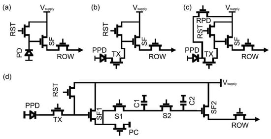
Figure 1.
Pixel circuit schematic of (a) 3T, (b) 4T, (c) 5T, and (d) 8T GSI pixel.
With the development of pinned photodiode (PPD) technology, a 4T GSI pixel process is developed, which can effectively inhibit Johnson–Nyquist (KTC) noise and obtain high voltage gain [9]. Compared with the original 3T GSI pixel, the new 4T GSI pixel used PPD instead of PD and added a charge Transfer transistor (TX). Due to the low noise and high output image signal, the 4T pixel has become the mainstream pixel structure. Since that, many novel pixel architectures have been developed based on this structure. For example, for a 5T GSI pixel, a separate exposure control transistor is added next to PPD to provide global exposure, which is more suitable for an ultra-fast working environment. Furthermore, in order to obtain Correlated Double Sampling with a lower noise level, an 8T GSI pixel structure for high-quality image applications is developed. Figure 2 illustrates the typical cell layout of an 8T GSI pixel. Since the global shutter pixel needs to store the signal inside the pixel, the pixel cell size of the high-performing voltage domain is usually more than five microns [10], resulting in a decrease of the resolution of the image sensor in the unit area. Moreover, the high-performance voltage-domain global pixel unit needs to integrate far more transistors than the conventional 4T rolling shutter pixel unit, resulting in a decline in the performance of the pixel unit. At the same time, the demand for high-quality application scenarios further puts higher requirements for dark current.
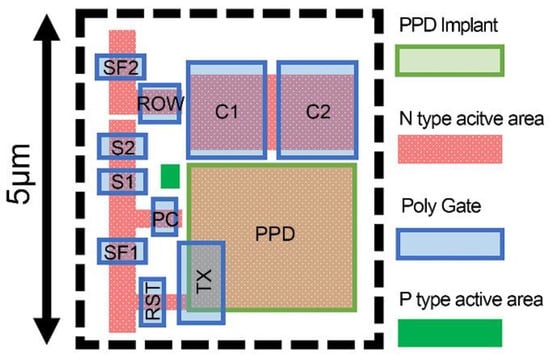
Figure 2.
A typical cell schematic layout of an 8T GSI pixel.
In this work, a novel 9T GSI pixel with the smallest pixel cell size is designed and fabricated. Moreover, the active region merging technique is used to optimize the dark current of the global pixel cell for the first time.
2. Structure and Working Principle
Figure 3 shows the circuit schematics of the designed 9T GSI pixel. The transfer transistor (TX) connects the PPD and floating drain node. The RST is used to reset the PPD. The source follower SF1 is used to amplify the signal generated by incident light. The PC transistor is used as the current source load of SF1. The switching transistors S1 and S2 combined with the capacitors C1 and C2 are used to collect the reset signal and the photoelectrical converted signal. The source follower SF2 buffers the sampled signal to the column bus. Finally, the ROW select transistor reads out the pixels.
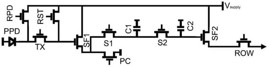
Figure 3.
Pixel circuit schematic of designed novel 9T GSI pixel.
Compared to the conventional 8T global shutter pixel in Figure 1d, the designed 9T global shutter pixel in Figure 3 added a Reset photodiode (RPD) transistor. The role of RPD in the pixel is to prevent highlight overflow. Because the full well charge of the photodiode of each pixel unit is specific, the photodiode will enter the saturation state under strong light or long-time exposure. When the charge cannot be stored in the photodiode, it will overflow to the adjacent pixel unit, resulting in the signal distortion of the surrounding unsaturated pixel unit. Therefore, adding a spillover prevention transistor to the photodiode of the 8T global pixel cell is necessary. When the photodiode is saturated, the excess charge can be discharged through an RPD transistor, and finally, the charge is removed from the voltage supply terminal.
As shown in Figure 4a, shallow trench isolation (STI) is usually used as the physical isolation between pixels. However, the STI process requires a plasma etching process, which will cause plasma damage on the side walls of the trench. Although an annealing process is added immediately for defect removal, many defect energy levels are still generated on the Si-SiO interface [11,12]. Moreover, when the defect energy level distribution is close to the depletion region, a large amount of dark current will occur, and the performance of the pixel unit will be degraded.
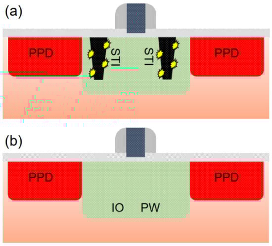
Figure 4.
The schematic cross-section of GSI pixel with (a) STI and (b) merged active area.
In order to modify the dark current rise brought by the STI process, we put forward a method that merges active area, as shown in Figure 4b.
The shallow trench isolation area in the pixel unit is completely removed through the layout design. In order to prevent the crosstalk between the two photodiodes, the adjacent photodiodes are isolated by IO PW, that is, 3.3 V P-well implant.
By removing the STI process, the damage to the interface caused by plasma etching and the rise of dark current can be avoided. Since PD is a light N-type implant, we can form a PN junction isolated by an isolated P well (IO PW) implant.
Figure 5 exhibits the layout of the designed 9T GS pixel. In order to prevent the STI from affecting the dark current performance of the pixel unit, the active area of the entire pixel array is merged into one block, that is, all the shallow trench isolation structures in the pixel unit are removed. The transistors are defined by heavily doped N-type implant and ploy gate. The grounding of the Vss node is achieved by heavily doped P-type implant. The PPD region is lightly doped N-type implant using phosphorus or arsenic. The P-type implant area of IO PW is generated by logical operation—the whole active area minus PD implant area. The IO PW realizes the PN junction isolation between the heavily doped N-type implant region and the PD implant area.
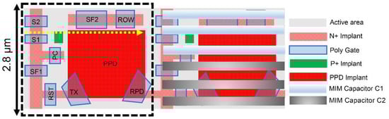
Figure 5.
The schematic layout of the designed 9T GS pixel.
In this pixel, the source follows transistors SF1 and SF2 and the bias transistor PC operate in the saturated region, and the ROW selection transistor ROW operates in the linear region so that the pixel output voltage can linearly follow the sampling voltage on C2. As shown in the right cell of Figure 5, two capacitors C1 and C2, store the reset signal and the electrical signal after photoelectric conversion. C1 and C2 in this paper use MIM (Metal Insulator Metal) capacitance. Since the MIM capacitance is formed in the back-end interconnects layer, it does not occupy the active area. Moreover, its area can occupy the entire 2.8 μm pixel unit, effectively increasing the capacitance value and reducing the noise. MIM capacitors, different from MOS capacitors, will not respond to the incident light, and the use of low leakage and high dielectric constant materials as capacitor dielectric layer makes the pixel unit noise smaller.
In order to realize the merging of the active area of the pixel unit, it is necessary to remove the area of the STI between the active areas, but at the same time, it is necessary to pay attention that some heavily doped area in the pixel will diffuse to each other and cause higher junction leakage and dark current. It is found the heavily doped P+ area will touch the heavily doped N+ area without shallow trench isolation. Therefore, it is necessary to define the minimum space between the N+ and P+ areas after active area merging.
The results obtained through the research are as follows. As shown in Figure 6, the two adjacent areas are implanted by heavily doped N-type and P-type implants. Even though there is a certain distance between the N+ and P+ areas on the layout, since the STI isolation is removed, the N+ and P+ area will be connected after the final diffusion, forming a heavily doped PN junction. This part of the PN junction leakage may be collected by the PPD, causing the unwanted dark current. The ideal PN junction reverse bias current equation is shown as follows:
where are the minority carrier concentration, are the minority carrier diffusion length, are the diffusion coefficient, is the minority carrier lifetime, are the distance from the edge of the depletion region to the corresponding electrode.
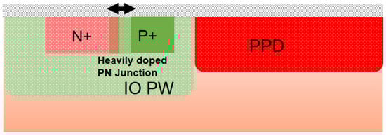
Figure 6.
The cross-section schematic of the yellow arrow in Figure 5.
When N+ and P+ area is close to each other, where , the formula can be simplified as follows:
When P+ and N+ are far apart and w′ > L, the reverse bias current of the PN junction can be simplified to the following equation:
From the above equation, we can know that when the PN region is far away, the recombination in the depletion region can be ignored. At this time, electrons and holes should be used as the diffusion lengths Ln and Lp of the minority carriers to replace the width of the depletion region, that is, Ln, Lp ≫ , so the reverse bias current is small.
The impact of the active merging on dark current was evaluated and analyzed. Based on the changes in the dark current after the merger of active regions, in order to ensure that the leakage performance of the pixel before and after the merger remains unchanged, the original N+ implant and P+ implant space need to be increased.
Since the PN junction reverse bias current is inversely proportional to the width of the depletion region, to avoid this risk, the spacing between the N+ and P+ areas should be increased as much as possible. We carry out layout split to get minimum design rules between the P+ area and the N+ area without increasing the leakage current.
3. Experimental Results
3.1. Effect of the Merged Active Area on a Single Transistor
At first, we evaluate the effect of the merged active area on a single transistor. As shown in Figure 7, taking NMOS transistors commonly used in CMOS image sensors as an example, the layout levels commonly used include active area (Active), polycrystalline gate (Poly), N+ implantation, P+ implantation, and contact hole (CT). For the sake of illustration, subsequent metal interconnection layers are not marked in the schematic. The area where the active area and the polycrystalline gate overlap is the channel part of the transistor, which is doped through the P well implantation and defines the turn-on voltage of the device and defines the source and drain of the transistor through N+ implantation. The part other than the active region in the conventional transistor structure is the STI region for isolation, and the formation process of the STI requires the use of a dry etching process, which often causes plasma damage on the STI sidewall. The damage will increase trap charges and interface state defects, which will lead to increased leakage of MOS devices and eventually, increase the dark current of the pixel unit.
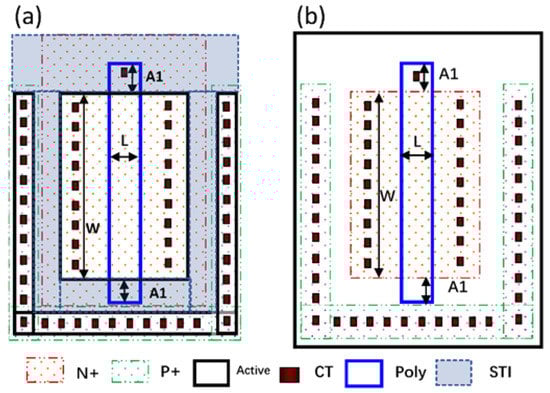
Figure 7.
The schematic layout of a single transistor with (a) STI and (b) merged active area.
In order to avoid the rise of dark current and the degradation of pixel performance caused by the STI used by conventional transistors, we can use the transistors whose active regions are merged, as shown in Figure 7b.
The active area is expanded to encompass all poly gate area, and the N+ implant area is reduced to the active area size of the conventional transistor. The channel region of the merged active area transistor is defined by the overlapping part of N+ implant area and poly gate area. The direction of the transistor current is the channel length direction, and the direction perpendicular to the channel length direction is the channel width direction.
The industry evaluates the performance of MOS devices, which are generally characterized by three items: Threshold voltage, off-state leakage, and saturation current, which reflect well ion implantation, physical size of active area and poly gate, thickness of gate oxide, and ion implantation damage. The commonly used MOS device parameter test adopts the industry’s conventional test method as follows:
- (1)
- Connect the substrate (B terminal) and source terminal (S terminal) to 0 V, apply a fixed voltage of 0.1 V to the drain terminal (D terminal), apply a step of 0.05 V to the gate oxide (G terminal), and scan from 0 V to 3.3 V voltage, take the VG value when ID is equal to 0.1 μA multiplied by the W/L value as the turn-on threshold voltage value (VT);
- (2)
- Connect the substrate (B terminal) and source terminal (S terminal) to 0 V, apply a fixed voltage of 3.3 V to the drain terminal (D terminal), apply a step of 0.05 V to the gate oxide (G terminal), and scan from 0 V to 3.3 V voltage, the ID value when VG is equal to 0 V is taken as the off-state leakage (Ioff) of the device, and the ID value when VG is equal to 3.3 V is divided by the channel width W as the saturation output (Idsat) of the device.
In this paper, the single transistor evaluation adopts the device size commonly used in pixel units, that is, the fixed channel width W = 0.4 μm, and the channel length layout split L = 0.28, 0.38, 0.48, and 0.58 μm. Due to the diffusion effect after ion implantation, the conductive channels may also be generated under the “A1” part of the merged MOS device POLY, so a layout split of A1 from 0.15 to −0.06 μm was designed to study the influence of the diffusion effect.
Figure 8 exhibits the characteristic transfer curves of the transistor with a width of 0.4 μm and length of 0.58 μm. It can be found that the device works properly after merging the active area under both 0.1 and 3.3 V Vd. However, the curve shifted slightly to the right, indicating that the threshold voltage increased slightly after merging the active area.
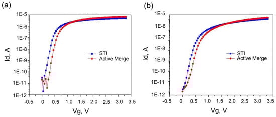
Figure 8.
The effect of Merged active area on Id vs. Vg curves in a single transistor under (a) Vd = 0.1 V and (b) Vd = 3.3 V.
Then, parameters VT, Idsat, and Ioff of MOS devices with sizes of W/L = 0.4/0.28, 0.4/0.38, 0.4/0.48, 0.4/0.58 μm before and after the active region merging were tested. Three devices of each size were tested on silicon wafers and their average value was taken for analysis. As shown in Figure 9a, VT increases after the active region is merged, and the VT of the four devices increases by 0.228, 0.184, 0.162, and 0.158 V, respectively, and the increase in VT decreases as the channel becomes longer. As shown in Figure 9b, the Idsat increases by 5%, 17%, 22%, and 26%, respectively, after the active region is merged. The increase ratio increases with the length of the channel. As shown in Figure 9c, after the active region is merged, the leakage current Ioff can be effectively improved, especially when the channel length is smaller.
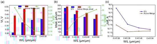
Figure 9.
The effect of the merged active area on (a) Vt, (b) Idsat, and (c) Ioff in a single transistor.
As mentioned above, Vt increased after merging the active area. Moreover, the leakage current decreased after active area merging.
Figure 10 shows the TCAD simulation structure of a single transistor with (a) STI and (b) merged active area (the simulation results in Figure 10 compare the AA merge device and the device with STI, and the white line in Figure 10c,d is the boundary of the depletion region). For the site near the STI in the channel of transistor, there is not only a vertical electric field from the gate oxide above but also an electric field at the edge perpendicular to the side wall of STI. This additional lateral electric field makes the area more prone to depletion, and the relatively lower gate voltage can create an inversion layer. As shown in Figure 10c,d, the depletion region of the transistor with the merged active area does not deepen at the channel edge, while the transistor with STI shows a deeper depletion layer thickness than that at the center. This results in a slightly higher Vt after merging the active area.
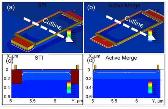
Figure 10.
TCAD simulation structure of a single transistor with (a) STI and (b) merged active area. (c,d) are the cross-sections at the corresponding cutline in (a,b).
The phenomenon that the depth of the depletion region increases when the channel is close to the STI boundary is not only caused by the fringe electric field but also related to the decrease of the concentration of boron near the silicon-oxygen interface during thermal diffusion. Moreover, the dopant atoms participating in thermal diffusion will have a concentration difference at the silicon-oxygen interface due to the inconsistency of their solid solubility in silicon and silicon dioxide.
For active region merged devices, there is no STI at the channel sides and the boron concentration does not decrease at the channel sides. Therefore, it can be expected that the AA merge device does not have the narrow width effect in the traditional sense.
At the same time, Idsat has also increased after merging the active area. The increase of Idsat is more significant with the increase in channel length. More importantly, the Ioff is significantly improved. The smaller the channel length, the more pronounced the improvement. The merged active area can effectively improve the leakage under the short channel.
3.2. Effect of Merged Active Area on GSI Pixel
We used the 55 nm process technology to produce the traditional 8T and the novel 9T GSI pixel. According to the incident light collection method, the image sensor process can be divided into FSI (front side illumination) manufacturing process and BSI (backside illumination) manufacturing process. The traditional 8T uses the FSI process, and the novel 9T GSI pixels use BSI process. The schematic layout of the fabricated traditional 8T is shown in Figure 2. The traditional 8T and novel 9T GSI structures have the same pixel array size, which is 2048 × 2048. Figure 11 exhibits the chip of the designed novel 9T GSI pixel after packaging.
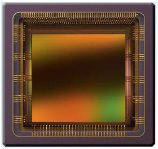
Figure 11.
The chip of the designed novel 9T GSI pixel after packaging.
Table 1 is the summary of characteristics and comparison with the previous reports. In this work, a novel 9T GSI pixel with a pixel pitch reduced to 2.8 μm is developed by combining the design of active region and MIM capacitance. The MIM will not occupy the photodiode area since it is formed in the back-end of line process. It means that MIM can change the pixel structure from 2D to 3D, and pixel size can reduce from 5 to 2.8 µm, which has 70% area saving. A smaller pixel size can improve the resolution of CMOS image sensor. Meanwhile, the backside illumination manufacturing process is necessary for this novel 9T GSI pixel since the MIM will block the incident light from the front side. The sensitivity of 2.8 μm 9T GSI pixel is 3.6 V/lx·S, which is comparable with 5 μm traditional GSI pixel.

Table 1.
Summary of characteristics and comparison with previous reports.
The dark current of 8T traditional GSI pixel is 68 e−/s. However, the dark current of 9T GSI pixel almost halved to 38 e−/s after the active area merged. The dark current will influence the image quality, especially in the lower light level and higher temperature environments. The image captured by traditional 8T GSI is shown in Figure 12a. The higher dark current cause image quality to degrade. The higher resolution and quality of the images captured by the novel 9T GSI, as shown in Figure 12b, is direct evidence of reduced dark current.
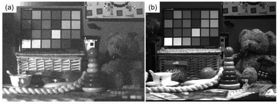
Figure 12.
Photographs captured by (a) traditional 8T GSI and (b) novel 9T GSI.
Moreover, the cross-talk of the novel 9T and traditional 8T GSI pixels are 20% and 19%, respectively, which is comparable. The cross-talk performance indicate the leakage path or diffusion path between adjacent pixels. Traditional 8T GSI pixel use shallow trench isolation and front side illumination process. The STI can provide physical isolation between pixels, but the front side illumination pixel has a thick substrate below the pixel area, which can be the diffusion path and cause cross-talk. The novel 9T GSI pixel use junction isolation to prevent the diffusion path between the adjacent pixels because there is no shallow trench isolation after the active area merged. Meanwhile, the novel 9T GSI pixel uses the backside illumination manufacturing process and deep trench isolation under the pixel area, which can prevent the pixel cross-talk effectively. Moreover, note that the active area merging is only happened in the pixel array and the peripheral circuit still use traditional shallow trench isolation which will not affect the normal transistor operation.
The read noise of the designed novel 9T GSI pixel is further reduced compared to the traditional 8T GSI pixel, from 8 e− to 5 e−. The designed 9T GSI pixel has a higher dynamic range than the traditional 8T GSI pixel, which is 62.9 dB (12 bit). The signal of the traditional 5 µm 8T voltage domain global shutter pixel is stored with MOS (Metal Oxide Silicon) capacitors. The capacitance of MOS capacitor is limited since it will occupy the pixel area. However, MIM (Metal Insulator Metal) capacitor can occupy the whole pixel area since it is above the pixel. Meanwhile, the MIM of the novel 9T GSI pixel uses a thinner and high-k dielectric for insulator to increase the capacitance. The bigger capacitance of MIM capacitor can reduce the read noise and improve the dynamic range.
Compared with those reported in the literature [13,14], the pixel pitch and dark current are the smallest. In addition, the cross-talk, sensitivity, read noise, dynamic range, and full well capacity also show good performance.
4. Conclusions
We have presented a novel 9T global shutter pixel with a merged active area. The minimal pixel pitch of 2.8 μm is achieved by using an MIM capacitor instead of a conventional MOS capacitor. The smallest dark current 38 e−/s is obtained by merging the active area. The cross talk of the novel 9T GSI pixel is 19% which is comparable to traditional 8T GSI pixel. The novel 9T global shutter pixel shows lower read noise and higher dynamic range because of the higher capacitance of MIM. The sensitivity of 2.8 μm 9T GSI pixel is 3.6 V/lx·S, which is comparable with 5 μm traditional GSI pixel. At the same time, the full well capacity also shows good performance, which is 7000 e−.
Author Contributions
Conceptualization, Q.S.; Investigation, X.G.; Resources, L.C.; Writing—review & editing, H.Z.; Supervision, D.W.Z. All authors have read and agreed to the published version of the manuscript.
Funding
This work was supported by the National Key Research and Development Program of China (2018YFB2202800) and the Program of Shanghai Subject Chief Scientist (18XD1402800).
Data Availability Statement
The data presented in this study are available on request from the corresponding author.
Conflicts of Interest
The authors declare no conflict of interest.
References
- Cha, H.-K.; Zhao, D.; Cheong, J.H.; Guo, B.; Yu, H.; Je, M. A CMOS High-Voltage Transmitter IC for Ultrasound Medical Imaging Applications. IEEE Trans. Circuits Syst. II Express Briefs 2013, 60, 316–320. [Google Scholar] [CrossRef]
- Mutoh, S.; Shigematsu, S.; Matsuya, Y.; Fukuda, H.; Yamada, J. A 1 V multi-threshold voltage CMOS DSP with an efficient power management technique for mobile phone application. In Proceedings of the 1996 IEEE International Solid-State Circuits Conference. Digest of TEchnical Papers, ISSCC, San Francisco, CA, USA, 10 February 1996. [Google Scholar] [CrossRef]
- Prasad, D.; Nath, V. Design of CMOS Integrator Circuit for Sigma Delta ADC for Aerospace Application. In Industry Interactive Innovations in Science, Engineering and Technology; Springer: Singapore, 2018; pp. 377–383. [Google Scholar] [CrossRef]
- Samanta, S.; Tiwari, B.; Bahubalindruni, P.G.; Barquinha, P.; Goes, J. Threshold voltage extraction techniques adaptable from sub-micron CMOS to large-area oxide TFT technologies. Int. J. Circuit Theory Appl. 2017, 45, 2201–2210. [Google Scholar] [CrossRef]
- Fossum, E.R.; Hondongwa, D.B. A Review of the Pinned Photodiode for CCD and CMOS Image Sensors. IEEE J. Electron Devices Soc. 2014, 2, 33–43. [Google Scholar] [CrossRef]
- Liang, C.-K.; Chang, L.-W.; Chen, H.H. Analysis and Compensation of Rolling Shutter Effect. IEEE Trans. Image Process. 2008, 17, 1323–1330. [Google Scholar] [CrossRef] [PubMed]
- Yadid-Pecht, O.; Pain, B.; Staller, C.; Clark, C.; Fossum, E. CMOS active pixel sensor star tracker with regional electronic shutter. IEEE J. Solid-State Circuits 1997, 32, 285–288. [Google Scholar] [CrossRef]
- Reiner, T.; Mishori, B.; Leitner, T.; Horovitz, A.; Vainbaum, Y.; Hakim, M.; Lahav, A.; Shapira, S.; Fenigstein, A. CMOS image sensor 3T Nwell photodiode pixel SPICE model. In Proceedings of the 2004 23rd IEEE Convention of Electrical and Electronics Engineers in Israel, Tel-Aviv, Israel, 6–7 September 2004; pp. 161–164. [Google Scholar]
- Lauxtermann, S.; Lee, A.; Stevens, J.; Joshi, A. Comparison of global shutter pixels for CMOS image sensors. In Proceedings of the 2007 International Image Sensor Workshop, Ogunquit, ME, USA, 6–10 June 2007; p. 8. [Google Scholar]
- Ho, J.-S.; Chiang, M.-C.; Cheng, H.-M.; Lin, T.-P.; Kao, M.-J. A new design for a 1280/spl times/1024 digital CMOS image sensor with enhanced sensitivity, dynamic range and FPN. In Proceedings of the 1999 International Symposium on VLSI Technology, Systems, and Applications, Taipei, Taiwan, 10 June 1999; Proceedings of Technical Papers. (Cat. No. 99TH8453). pp. 235–238. [Google Scholar]
- Kwon, H.I.; Kang, I.M.; Park, B.-G.; Lee, J.D.; Park, S.S. The Analysis of Dark Signals in the CMOS APS Imagers from the Characterization of Test Structures. IEEE Trans. Electron Devices 2004, 51, 178–184. [Google Scholar] [CrossRef]
- Moon, C.-R.; Jung, J.; Kwon, D.-W.; Yoo, J.; Lee, D.-H.; Kim, K. Application of Plasma-Doping (PLAD) Technique to Reduce Dark Current of CMOS Image Sensors. IEEE Electron Device Lett. 2007, 28, 114–116. [Google Scholar] [CrossRef]
- Sekine, H.; Kobayashi, M.; Onuki, Y.; Kawabata, K.; Takahashi, H.; Inoue, S.; Ichikawa, T. A high optical performance 3.4 μm pixel pitch global shutter CMOS image sensor with light guide structure. In ITE Technical Report 41.32 Information Sensing Technologies (IST); The Institute of Image Information and Television Engineers: Tokyo, Japan, 2017; pp. 5–8. [Google Scholar]
- Velichko, S.; Hynecek, J.J.; Johnson, R.S.; Lenchenkov, V.; Komori, H.; Lee, H.-W.; Chen, F.Y.J. CMOS Global Shutter Charge Storage Pixels with Improved Performance. IEEE Trans. Electron Devices 2015, 63, 106–112. [Google Scholar] [CrossRef]
Disclaimer/Publisher’s Note: The statements, opinions and data contained in all publications are solely those of the individual author(s) and contributor(s) and not of MDPI and/or the editor(s). MDPI and/or the editor(s) disclaim responsibility for any injury to people or property resulting from any ideas, methods, instructions or products referred to in the content. |
© 2023 by the authors. Licensee MDPI, Basel, Switzerland. This article is an open access article distributed under the terms and conditions of the Creative Commons Attribution (CC BY) license (https://creativecommons.org/licenses/by/4.0/).