Article

Software Engineering of Resistive Elements Electrophysical Parameters Simulation in the Process of Laser Trimming

by
Vladimir V. Kondrashov
1,2,*,
Oleg S. Seredin
3,
Vyacheslav V. Chapkin
1,
Evgeny V. Zemlyakov
2 and
Ilya K. Topalov
2
1
Department of Microelectronics, Public Joint-Stock Company Scientific and Production Association Strela, 300002 Tula, Russia
2
World-Class Research Center Advanced Digital Technologies, State Marine Technical University, 190121 Saint Petersburg, Russia
3
Cognitive Technologies and Simulation Systems Lab, Tula State University, 300012 Tula, Russia
*
Author to whom correspondence should be addressed.
Electronics 2023, 12(3), 589; https://doi.org/10.3390/electronics12030589
Submission received: 14 December 2022 / Revised: 8 January 2023 / Accepted: 21 January 2023 / Published: 25 January 2023
(This article belongs to the Special Issue Feature Papers in Circuit and Signal Processing)

Abstract

:
This study continues a series of papers covering the R&D of circuit simulators embedded into manufacturing equipment for the laser trimming of film and foil resistors intended to improve the final product’s performance and reduce process costs. Our paper describes the development of the ResModel laser trimming simulation software. Various types of trims and their features are presented for a circuit with a dynamic measurement DC source, and the optimal trim configurations are identified. The software can be used to estimate and display resistive element properties during the trimming such as its electrophysical parameters and their trends.

1. Introduction

Any changes to manufacturing equipment or processes require test runs and final product testing. The equipment and the control logic are then fine-tuned, and the tests are repeated. This is the manufacturing process adjustment cycle. When the changes are significant, the process adjustment may be quite challenging both in terms of efforts (making test parts, running a pilot process, acquiring and analyzing the results) and the cost of consumables spent [1]. Moreover, it is often difficult to identify which process variable or equipment component affects the result.
For this reason, simulation software is required to assess the models, adjust the algorithms, and better investigate the distribution of resistive elements (RE) electrophysical parameters. It should be used before actually implementing the models of film or foil resistors proposed and described in detail by us [2,3], into the control systems of actual laser machines. Please refer to [2,3] for a detailed description of the proposed models.
There are many studies on the simulation of film and foil resistors, laser trimming, and dedicated simulation software.
Some of the film resistor simulation papers are of special interest. Wing Shan Tam et al. [4] investigate the adjustment of a composite resistor’s resistance by breaking the linked fuses. Phillip Sandborn and Peter A. Sandborn [5] present the options for emulating the trimming process with conductive paper and comparing the results with the simple analytical methods (the rectangle method) and giving the resistance vs. length of laser trim curves (the so-called resistor trimming curves, RTC). Sandborn, P. et al. in [6] present a detailed finite difference model of the film resistor and discuss the optimal trim paths for achieving the specified resistance in detail. The optimization criteria are the length of the trim and the final resistance accuracy. The paper also contains examples of the current load analysis over the entire resistor. We should also note that paper [6] compares the results of the trim simulation with the conductive paper experiments.
V. Sadkov, A. Pilkevich, K. Fomina, and E. Korshunova [7,8,9] extensively covered the conformal map-based simulation of resistors, absorbing elements, and embedded attenuators exposed to HF and UHF signals. A. Pilkevich et al. [10] confirm the results obtained with the proposed simulation methods. They compared the results with that produced by a general-purpose FEM simulation package for EM, thermal, and mechanical processes [11]. A. Walton, R. Holwill, J. Robertson [12], M. Horowitz, and R.W. Dutton [13] solved similar resistor simulation problems at microwave frequencies. Van der Woerd et al. [14] present a mathematical model and the results of computer calculations of resistance with Green’s boundary functions. M. Rubanovich, N. Aleksandrov, V. Manusov, and V. Khrustalyov [15] simulated the EM properties of film RE. They performed FEM and nodal stress calculations to determine the distribution of capacitance and inductance values along the cross-section of the film resistor. Matlab 2010 and the SimPowerSystems (SPS) library for Simulink were used for the numerical estimation of currents and voltages. The results produced by the proposed EM simulation model are confirmed by the electrodynamic calculation of the imaginary and real parts of the film resistor impedance performed with the Microwave Office.
The following works cover the development or application of resistor trim simulation software. Michael J. Mueller and Wes Mickanin [16] present the RAREA simulation results. The software calculates the resistance using the method of least squares. The software was written in Pascal and run on the RSTS, VMS, and Unix operating systems. RAREA can also design the RE configuration from the specified requirements for its geometry and properties. T. Mitsuhashi et al. [17] developed the RCALC simulator with the appropriate capabilities.
Papers [18,19,20] present the FIRE and SCANRES film resistor simulation packages. They evaluate the effect of the heat-affected zone (HAZ) around the laser cut on the accuracy of the expected resistance value. Among others, the packages estimate the relative dissipated power density over the entire resistor film. J. Shier. [21] gives a detailed overview of FEM applications to film resistor simulation. The author also presents a dedicated code in Basic. G. Papp in [22] gives a detailed description of the finite difference method and the simulation results as the software reports. They clearly show the resistance values and the current and power dissipations. P. Moran et al. [23] present the mathematical model and give a detailed description of the software features and capabilities for evaluating the resistance, the resistance sensitivity to trims, and the magnitude of local “hot spots”. They also give a case example. It should be noted that K. Schimmanz, A. Kost, and S.M. Jacobsen in [24,25,26,27] provide not only a detailed description of FEM, finite difference, and boundary element-based approaches but also compare the results in terms of accuracy and performance. Paper [28] presents an extensive list of parameters affecting the simulation results. They are the key properties of the RCutSim trim simulator developed by the paper’s authors. We also should mention a number of in-depth studies that resulted in the development of trim resistance estimation software or a full-fledged mathematical model [29,30,31,32].
The authors of [6,10,12,15] used general-purpose simulation software. S. Kaminski, E. Mis, M. Szymendera, and A. Dziedzic used ANSYS [33,34] to develop the new resistor configurations (with three pads) and laser trims. They also compared the simulation results with the actual trimming on the Aurel equipment [35]. The authors applied conformal mapping for calculations and claimed the results agree well with the FEM results. A. Manolescu et al. [36] used Matlab to estimate the resistance also using conformal mapping.
Some researchers give simulation results as predicted resistance values, current distribution diagrams across the resistor film, trim curves, or statistical values but do not specify what models and software they used. Studies [37,38] investigate the optimization of trim cut configurations. Y. Antonov [39] gives examples of analytically estimated resistance values compared to that of the trimmed RE [40]; J. Skácel [41] describes the prediction of the thick film resistor trimming.
Unfortunately, a large number of studies presented above contain a description of the solution of only a narrow specific problem, whether it is the construction of a resistor model or the development of a simulation program. Apparently, the authors of these works did not set the task of an integrated approach to automating the process of laser trimming and embedding models and algorithms in equipment. In addition, the authors of most studies, for all the undoubted significance of their work, either do not study the obtained models for accuracy (there is no comparison of the simulated value in the simulation system with the real values of the resistance of the trimmed resistors) or do not provide data on the efficiency of the calculation algorithms for the proposed models. Additionally, a number of researchers do not provide a description of the construction of the model, and, therefore, it is not possible to assess which of the methods was used.
Our detailed analysis of the above studies identified the need to develop a laser trimming simulation software to be used before embedding the existing models and algorithms [2,3] for calculating the electrophysical parameters of resistive films into the industrial equipment software. Such a system will enable the flexible modification and fine-tuning of the algorithms, a preliminary analysis of the model accuracy and adequacy, and studying the features of various resistor configurations. Additionally, a detailed description of the software structure and implementation of the existing models and algorithms will hopefully help researchers and engineers in this area with using and analyzing the results of this study.
This article has the following structure. The Introduction presents the prerequisites for this particular work within the framework of the general series of articles, analyzes the available literature, highlights the advantages and disadvantages of known works and approaches, presents the purpose of the work, and also provides the structure of the manuscript. Section 2, “The ResModel Software”, proposes a method for implementing the ResModel software based on the models and algorithms developed by the authors and provides a detailed internal structure of the program, as well as hardware requirements. Section 3 contains an example of the program with a detailed presentation of internal variables, as well as initial data and simulation results. Section 4 describes in detail the features of the software implementation of the representation of the laser spot, gradient filling, as well as solving systems of linear algebraic equations. Section 5 contains the results of the simulation modeling of the process of trimming a resistive element with various types of trimming cuts in order to illustrate the capabilities of the developed software. Section 6 discusses the results obtained. Section 7 gives an idea of the next steps of the research.

2. The ResModel Software

2.1. General

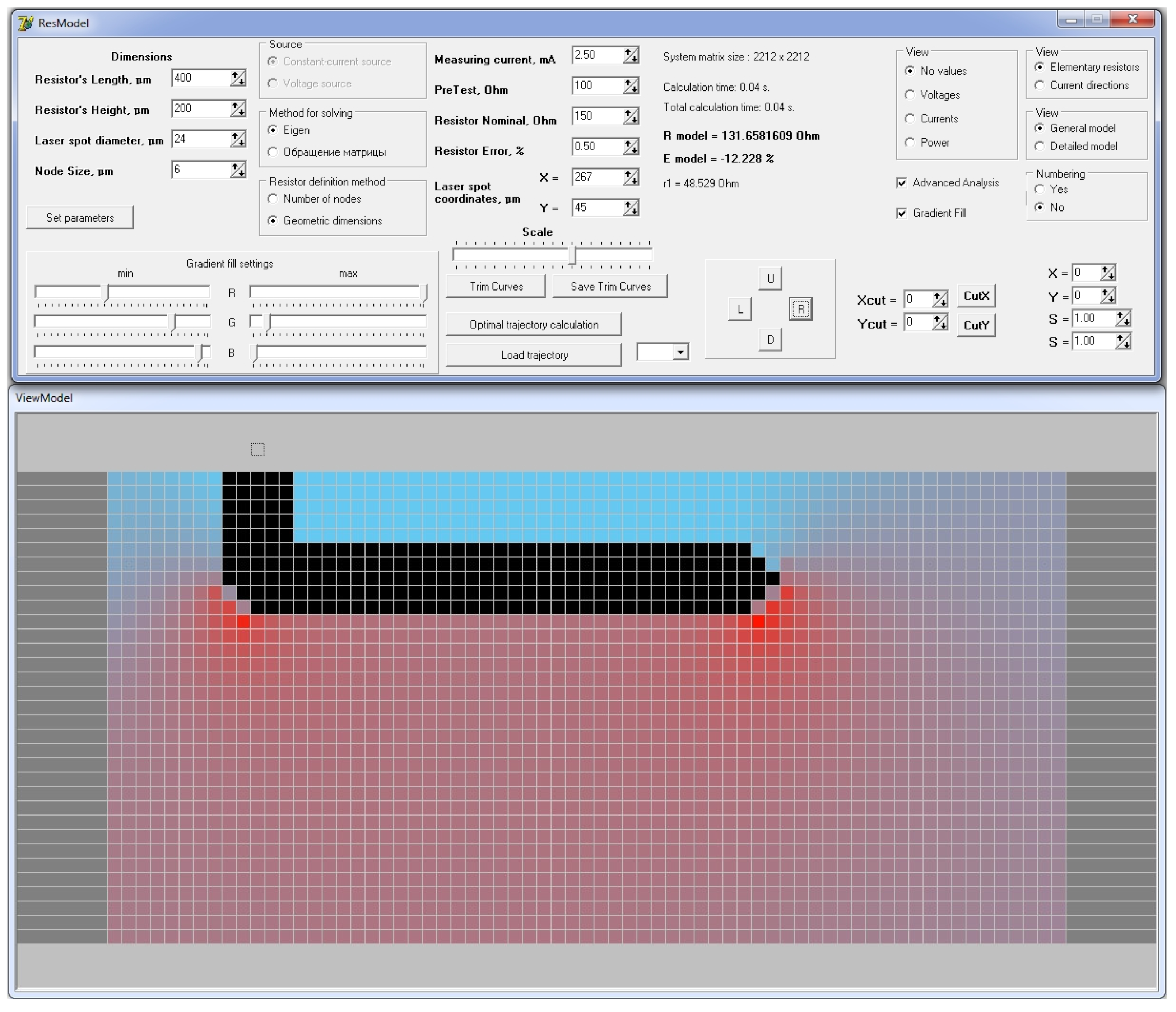
The simulation software we developed is a 32-bit Windows application written in Object Pascal (Borland Delphi 7.0 compiler). Figure 1 shows the main window.
The user interface is divided into two panes. The first pane contains the input and output fields and the settings. The second pane presents the results visually as a map of the RE with its contact pads/conductors. The user controls the simulation in the second pane: sections of the resistive film or foil are removed by a mouse click.
The ResModel’s key features are:
  • Simulation data input/editing;
  • Resistor trim simulation;
  • Setting up the simulation result options;
  • Generating the simulation results as the resistance of the resistor and its deviation from the rated value;
  • Plotting the resistor trim curves;
  • Rendering the current distribution pattern as a gradient fill;
  • Rendering the current direction field along the branches;
  • Rendering the voltage, current, and power values on the grid (graph) branches;
  • Generating the optimal trim path by minimizing the deviation of the resulting resistance from the rated value and providing the minimax solution for the power and current at the elementary resistors (ERs) making up the grid.
The ResModel input data are:
  • Resistor dimensions (length and width);
  • Laser spot diameter;
  • Grid node size;
  • Measuring current or voltage;
  • Pre-tested resistance value;
  • Resistor rating;
  • Acceptable resistance deviation from the rated value;
  • Resistor width after trimming.
Minimum PC requirements:
  • CPU: 2nd gen Intel® Core™ i5 processor or equivalent;
  • RAM: 2 GB;
  • 1024 × 768, SVGA card, 32-bit color depth;
  • Keyboard and mouse;
  • Windows XP, Windows 7 operating system;
  • Free disk space: 10 MB.

2.2. Software Architecture

The software builds a model of the film or foil RE and the trim model from the user-defined input data. Table 1 lists the main model variables.
ResModel stores the resistor properties mostly as one-, two-, and three-dimensional arrays of both integer and floating-point numbers. The reason is that the model is best represented with a two-dimensional array. Moreover, the number of nodes and branches in the grid for a detailed model is very large, which may be challenging if other data structures are used. One object (for example, a branch) has multiple parameters: ER voltage and current, dissipated power, ER serial number, etc. The key variables and their descriptions are listed in Table 2. This paper features examples of a DC power source [2]. The slight differences in the matrix structures for a DC voltage source are presented in detail in [3].

3. ResModel Operation

To better present the main variables and arrays, we will consider an example: a trimmed resistor with the parameters listed in Table 3. At the same time, the dimensions of the resistor for demonstrating the operation of the software were chosen as close as possible to one of the smallest types among chip resistors—01005 (dimensions 0.4 mm × 0.2 mm). However, if a length of 0.4 mm were chosen, then the dimensions of the arrays Arr1, Arr2Br, Arr3Node, Arr3NodeI given later in this article would be higher, which would negatively affect the visibility of the information. The diameter of the laser beam spot was taken based on the technological requirements for microminiature resistors and the capabilities of modern equipment for laser trimming. The node size NodeSize is equated to the diameter of the spot, again for the sake of clarity of the matrices. The electrophysical parameters of the resistor in this example are chosen arbitrarily and do not have any effect on the contents of arrays Arr1, Arr2Br, Arr3Node as illustrations of the internal structure of the software.
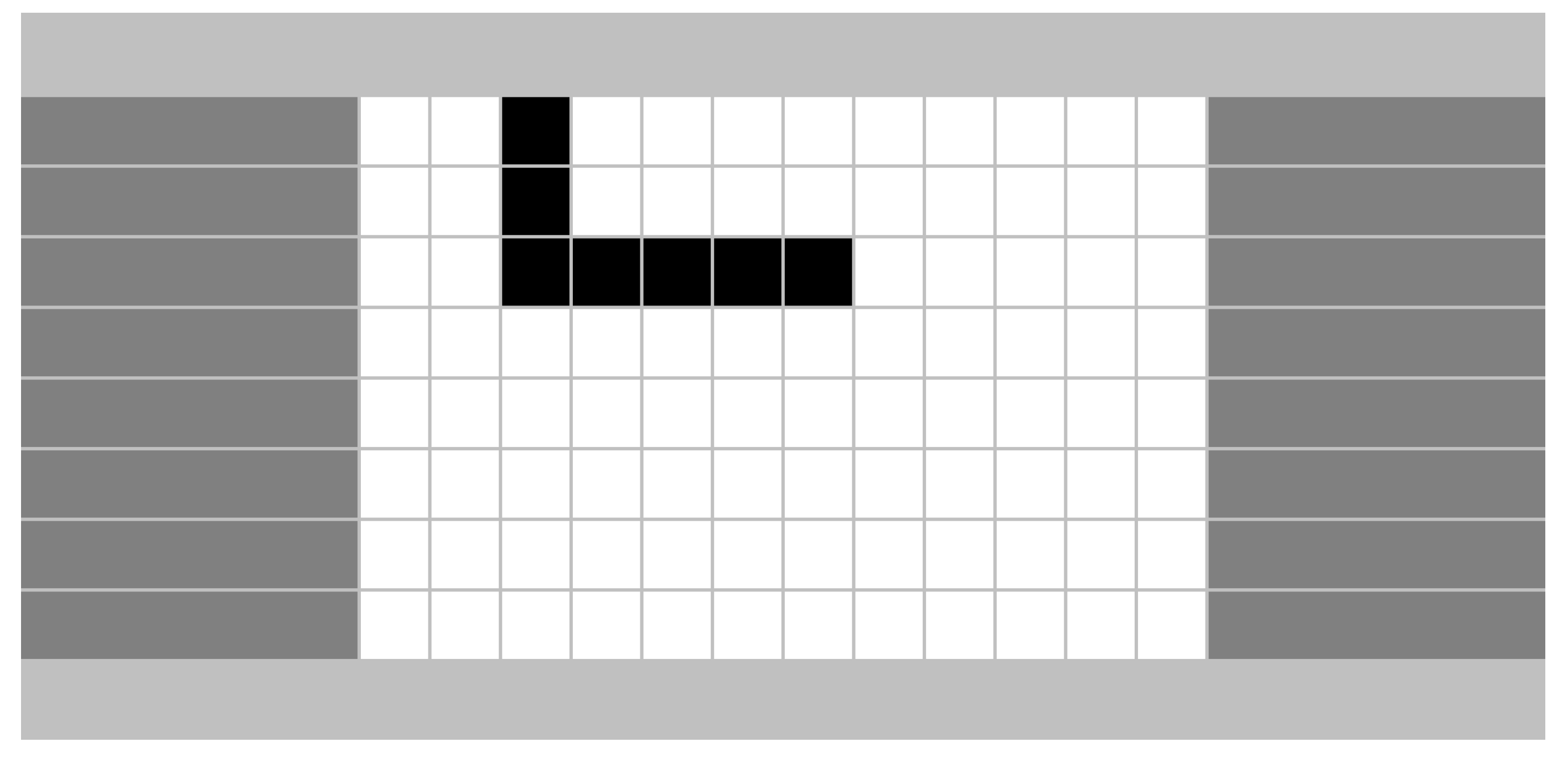
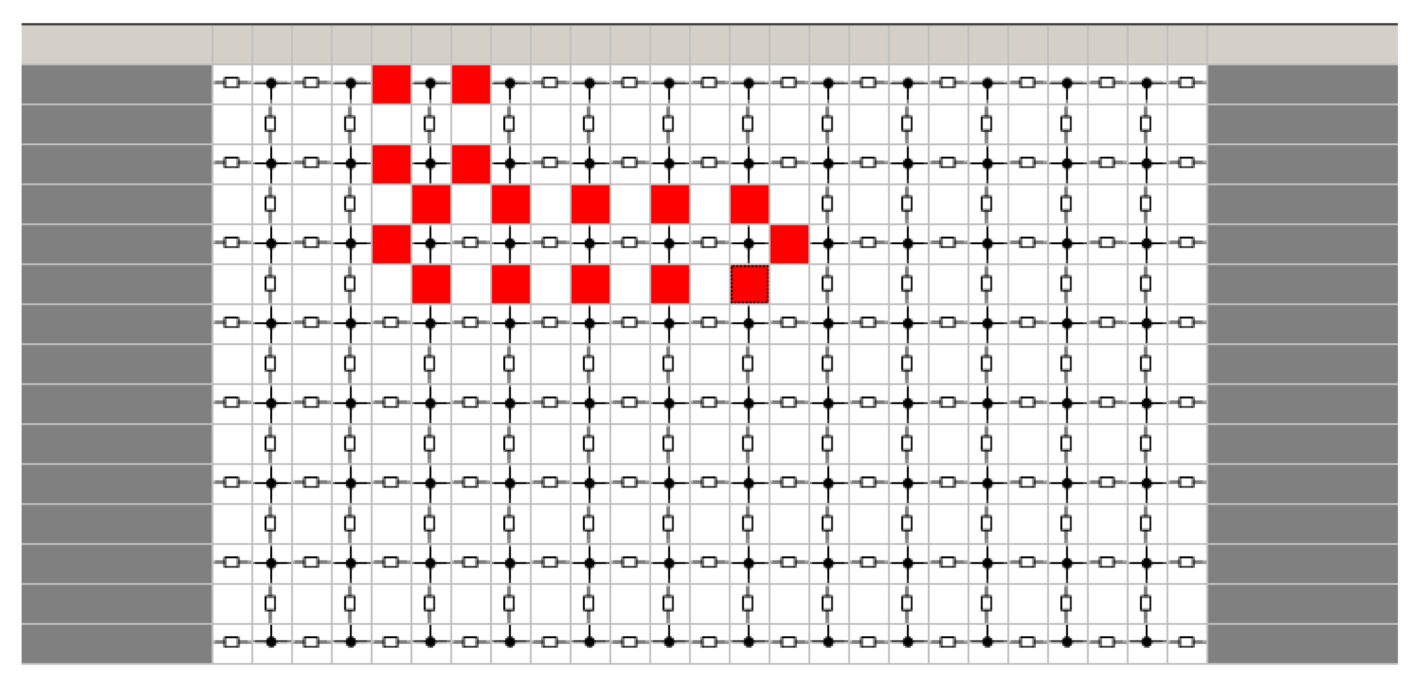
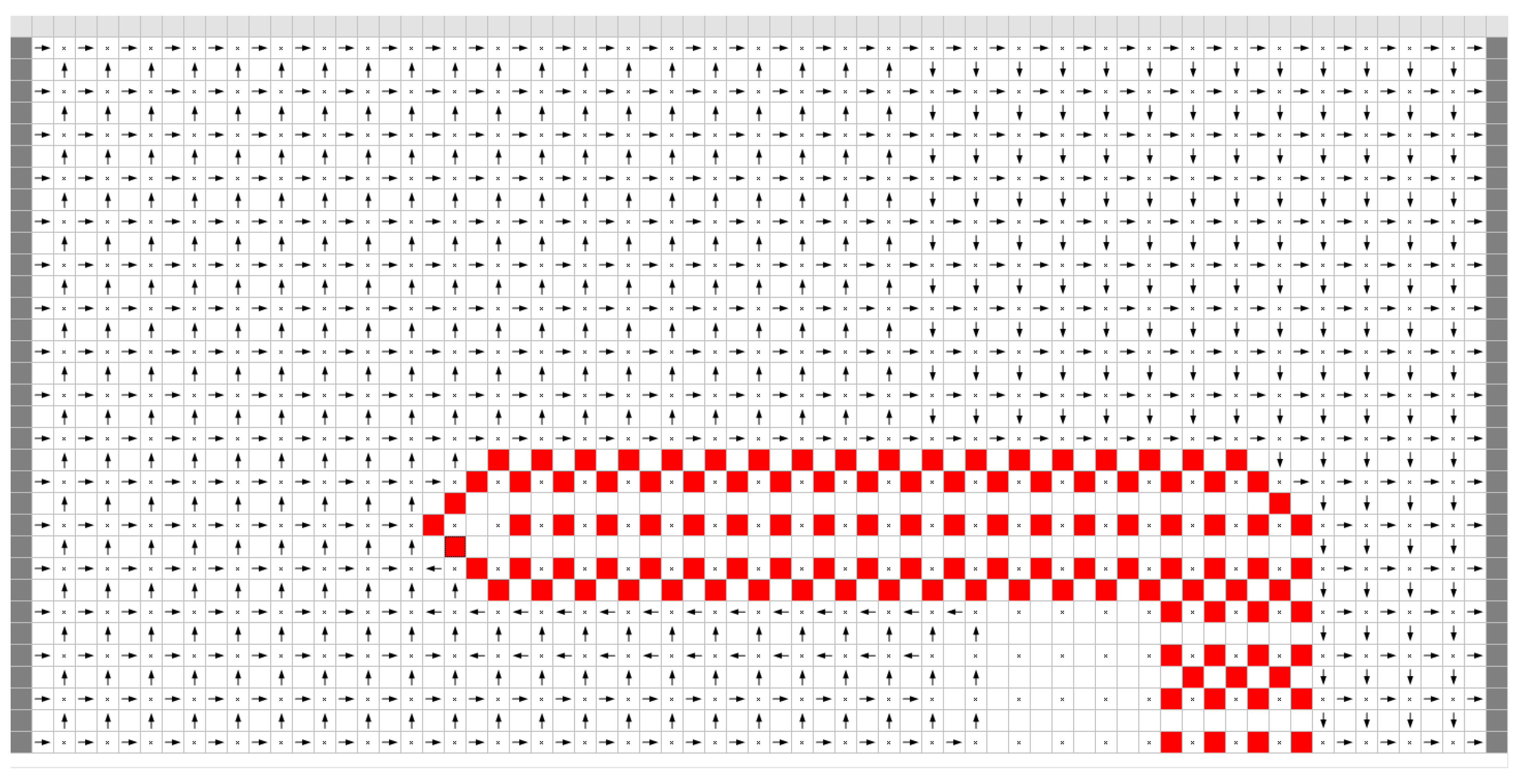
The resulting resistor model is shown in Figure 2 (general view) and Figure 3 (detailed view). At the same time, in both views, the dark areas located on the left and right imitate contact pads; above and below the body of the resistor are sections of the dielectric substrate. The trimming cut itself in Figure 2 is depicted in black on a white field of resistive material. In Figure 3, the trimming cut is depicted in red in more detail, illustrating which elementary resistors are removed from the grid circuit model when forming the general view of the cut in Figure 2.
The dimensions of the arrays are listed in Table 4. The table also contains the main characteristics of the internal model representation.
The Arr1 array is shown in Table 5.
This matrix is intended to provide an internal representation of the grid circuit model in detail (as shown in Figure 3). Row 0 and column 0 store ordinal numbers and are omitted as trivial here and in some of the following matrices where they are used in the same way. The node numbers are stored at the intersections of odd-numbered rows and even-numbered columns. The cells at the intersection of even-numbered rows and columns, and odd-numbered rows and columns, contain one if there is a branch and zero if the ER corresponding to the branch has been trimmed. All the other cells are zeros.
The Arr2Br matrix contains the numbers of branches at the intersections of even-numbered rows and even-numbered columns and odd-numbered rows with odd-numbered columns. The unused cells are zeros. The Arr2Br matrix for the example under consideration is shown in Table 6. Both the Arr1 matrix and the Arr2Br matrix are needed in general to ensure the end-to-end numbering of nodes and branches in accordance with the requirements for the nodal analysis method based on topological and component equations, which was described in detail in previous articles of the cycle shown in Figure 3 in [2], Figure 3 in [3].
The Arr3Node array is filled by sequentially analyzing the grid nodes using the information contained in the Arr1 matrix. If the number of “live” (conducting) branches connected to the node is greater than one, then the node is considered operational, and the corresponding matrix cell is set to one. Otherwise, it sets to zero.
Each cell of the Arr3NodeI array is filled only if the corresponding cell of the Arr3Node array contains one. The value stored is equal to the sum of the absolute currents in the branches adjacent to the node. If a node is not operational (the Arr3Node matrix contains zero in the corresponding cell), then the cell is also set to zero.
The Arr3Node and Arr3NodeI matrices for the ResModel simulation example are shown in Table 7 and Table 8, respectively. In the course of the program, these matrices serve as data storage for displaying the distribution of the current load over the sections of the resistive film.
The Y N system matrix is filled as previously mentioned in Section 4 in [2] and Section 4 in [3]. It contains the system structure (6), (11), and the number of nodes to which the resistor being trimmed is connected. If the k th branch with the y k conductivity which connects node i to node j is added, the matrix Y N is adjusted at four places: y k is twice added to the y i i и y j j elements of the Y N matrix diagonal, and y k is twice subtracted from the y i j and y i j non-diagonal elements:
Y N = i j i j + y k y k y k + y k
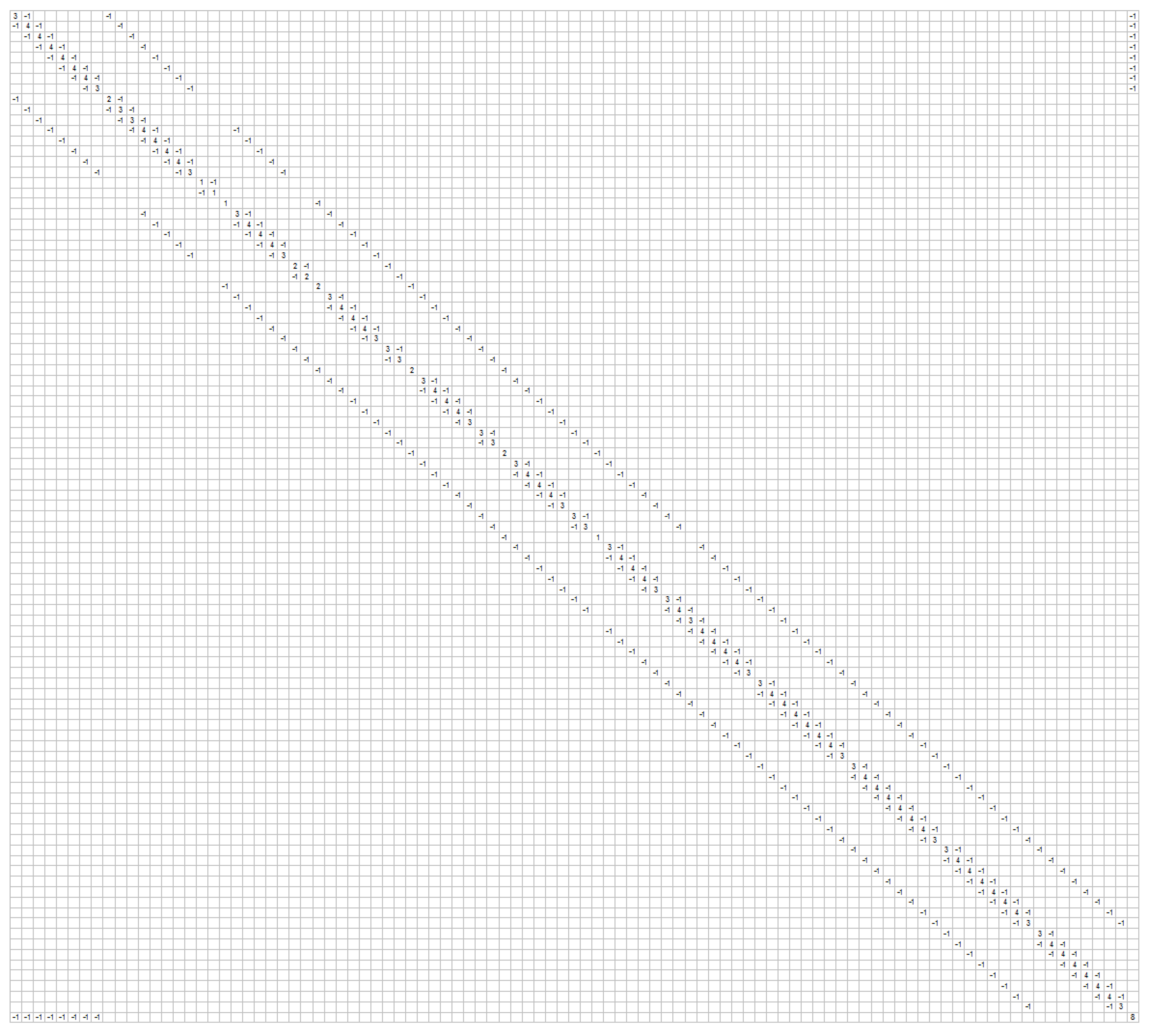
It reduces the required computer resources (time and memory) which would otherwise be required to create and handle the incidence matrix. Please refer to Figure A1 in Appendix A for the system matrix for this example. The incidence matrix is created when an extended analysis is needed, i.e., to calculate not only the resistance for a specific trim, but also the currents, voltages, and dissipated powers for all the ERs.

4. Overview of the Computational Algorithms—Results Visualization

4.1. Laser Spot Representation and the Effects of Laser Spot Size on the Simulation

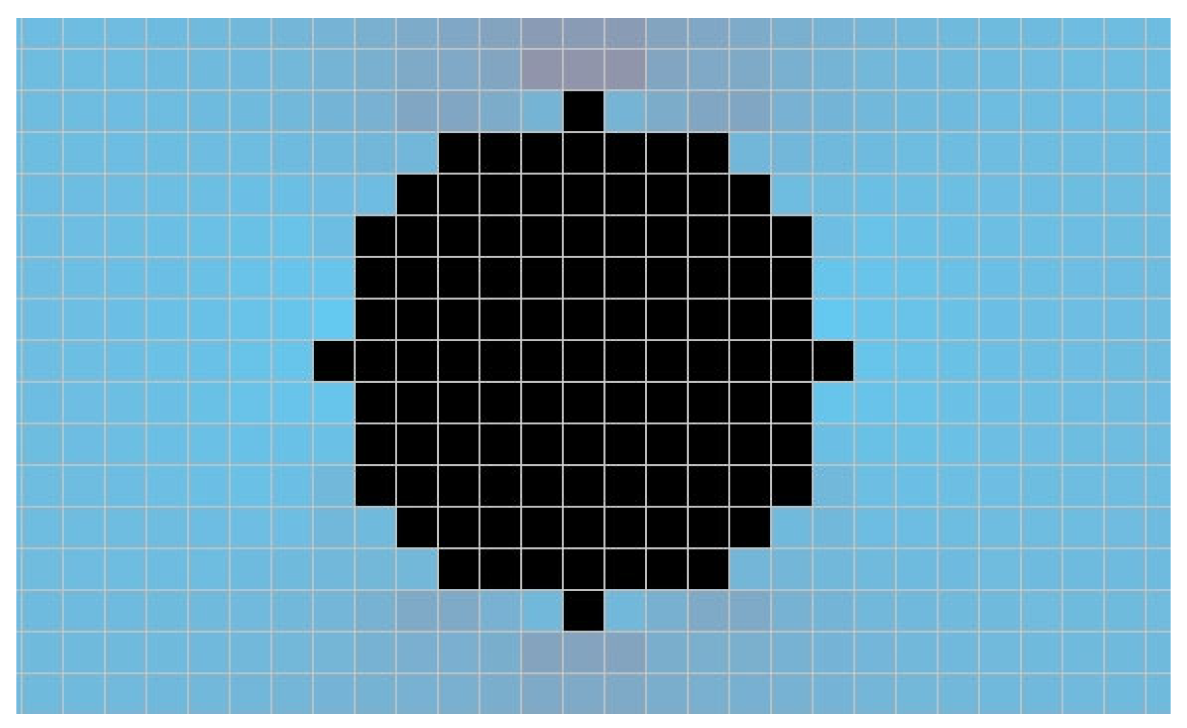
In the example above, we used the real dimensions of the resistor and the laser beam spot, but the NodeSize value is too large for such a resistor. Indeed, the node size variable (NodeSize) essentially specifies the number of increments for the discrete approximation of the resistor with the grid and the step of the laser beam movement used in the trim simulation. The node size also affects the laser spot shape.
A laser cut is created as follows. The user selects the trim starting point by clicking the mouse in the RE map pane. Then, the cut is progressed by clicking the joystick-like buttons. One click is one step in the corresponding direction. The cut is displayed on both the general and detailed maps.
The row and column numbers of the node at the laser spot center are calculated at each step. After that, the software locates the nodes within a square inscribed into the circle being the laser spot outline [42]. The laser spot (D diameter) is modeled by removing the nodes whose coordinates satisfy the following condition, from the square
i R o w 2 + j C o l 2 D 2 N o d e S i z e 2
where i , j are the row and column of the node in the Arr3Node matrix and R o w , C o l are the row and column of the central node in the laser spot.
As a result, as the movement step decreases, the shape of the spot gradually approaches a circle. Figure 4 shows an image of the laser spot on a simulated resistor for NodeSize = 2 μm, D = 24 μm.

4.2. Gradient Fill as a Visual Interpretation of the Current Load Distribution

The detailed model view can be set up to display not the ERs but the voltage, amperage, or power in the given branch, or the current direction (indicated by the arrow). Such a visualization makes it easier to analyze the current distribution over the resistor branches. The initial data are taken from the VUr, VI, and VP arrays (refer to Table 2).
The model can be rendered with a gradient fill to show the current load distribution. The gradient fill is applied as follows. From The Arr3NodeI array, we can find the total of the absolute current values in the branches adjacent to a non-trimmed node. First, the minimum and maximum values in this array are found. These can be represented as two points on a line. Let us match the start and end points ( I min and I max ) of the line ( L length) with the points in the 3D RGB color space: . A r 1 , g 1 , b 1 and . B r 2 , g 2 , b 2 . Then, the fill color of a pixel located at s from the origin, i.e., corresponding to the I arbitrary value (at that I min < I < I max ), is determined as follows:
r = r 1 r 1 r 2 s L g = g 1 g 1 g 2 s L b = b 1 b 1 b 2 s L
A sequential analysis of the Arr3NodeI matrix contents complements the general view (Figure 2) with the current load distribution over the resistive film (Figure 5).

4.3. Solving the System of Linear Algebraic Equations

We should pay special attention to solving the system of linear algebraic equations. For example, when the conducting layer of the resistive film is approximated by a discrete grid of ERs with n = 96 internal nodes and b = 188 branches, the A incidence matrix will have the size of 98 × 189 , and the Y N reduced matrix of nodal conductivities will have the size of 98 × 98 , as follows from Table 4. Therefore, the number of elements in matrix A is 18,522, and in matrix Y N , 9604. If we consider the real dimensions of the resistor, however, the size of the matrices will be much higher. For instance, one of the smallest standard dimensions of a precision thin-film lead-free chip resistor is 2 × 1.25 mm (0805 resistor size). If the focused laser spot diameter is 20 μm, an adequate model should have discrete nodes not exceeding 10 μm. Based on the equations, the number of internal nodes is n = 200 × 125 = 25,000 , and the number of branches is b = 49,925 . Even if we fill the Y N matrix not using the incidence matrix but by directly analyzing the interconnections between the nodes (to avoid operations with A matrices of the size 25,001 × 49,926 = 1,248,199,926 ), for solving the system of equations, the Y N matrix of nodal conductivities will have 25,001 × 25,001 = 625,050,001 elements.
The matrix Y N is highly sparse. We considered the methods and libraries for solving similar systems of linear algebraic equations [43,44,45,46,47,48,49,50] and studied the in-depth comparative analysis of available software libraries [51] and decided to use the Eigen library for all the calculations [52]. ResModel can also make calculations by exchanging the matrices, but it greatly reduces the performance.

5. Resistor Trimming Simulation

The resistance of a film or foil RE can be adjusted by trims with different leg lengths and different starting points. Multiple trims of the same type or a combination of trim types can be used to adjust a resistor.
Each type of trim path has its peculiar design and manufacturing considerations. This affects its applicability to a particular group of film resistors. For high-voltage resistors, a certain minimum distance between the trims shall be maintained, whereas for HF resistors, any trim paths increasing the intrinsic capacitance and inductance of the resistor shall be avoided. For precision REs, it is important to minimize their width variations.
Let us consider the most common trim types and their features based on the ResModel simulation results.

5.1. Types of Laser Trims

The trim configurations can be divided into simple and composite (combined). Figure 6 shows the simple types.
Legend for Figure 6:
  • Resistive film or foil;
  • I-cut (Plunge cut, or Dive cut);
  • L-cut;
  • J-cut;
  • U-cut;
  • S-cut (Shaving cut, or Scan cut).
The text continues. The composite trims consist of simple cuts. Their starting points can be on one or both sides of the RE. Figure 7 shows some composite trims.
Legend for Figure 7:
  • Resistive film or foil;
  • Ii-cut (double I and i cut, or Double Plunge cut);
  • Li-cut (double L and i cut, or Shadow cut);
  • W-cut (“Serpentine”).

5.2. Plotting and Analysis of the Resistor Trim Curves

We will simulate the trimming of a film resistor with the input data listed in Table 9.
Figure 8 shows the simulated resistor trimming curves.
The RTCs are resistance vs. laser trim length curves. The path length is measured in steps. One step is the size of a node.
With the RTC, we can draw the following conclusions. The I-cut takes the smallest number of steps to adjust the resistance to the rated value (Figure 8a). However, the resistance increase rate is the greatest; each step sharply raises the contribution of the remote nodes and branches. The L-cut trim (Figure 8b) provides a lower resistance increase rate. The curve for the first leg of the trim path is identical to that of the I-cut trim, whereas the second curve is nearly a straight line. The J-cut trim curve (Figure 8c) is identical to the L-cut trim curve but has a section corresponding to the third leg of the trim, where the resistance varies very slowly. For the U-cut (Figure 8d), the length of this leg is equal to the length of the first leg, whereas the contribution of the trimmed ERs tends to zero as the laser spot approaches the resistor edge. The S-cut (Figure 8e) shape is identical to the U-cut, but their curves are strikingly different. For composite cuts, the simple cut (base trim) is created first. For example, the L-cut is the base cut for the Li-cut. The second i-cut is then performed. For the W-cut, the central I-cut is created first, followed by two cuts on the opposite side of the RE.
The resistance curves for the basic legs of the Ii-cut and Li-cut trims are identical to that of the simple straight trims (Figure 8f,g); the double dive i-cut creates a small parabola at the end of the curve. The W-cut (Figure 8h) is a combination of I-cuts on opposite sides of the resistor. As a consequence, the RTC for each “serpentine” leg is similar to that of the I-cut trim.

5.3. Analysis of Current Distribution in the Film Resistor

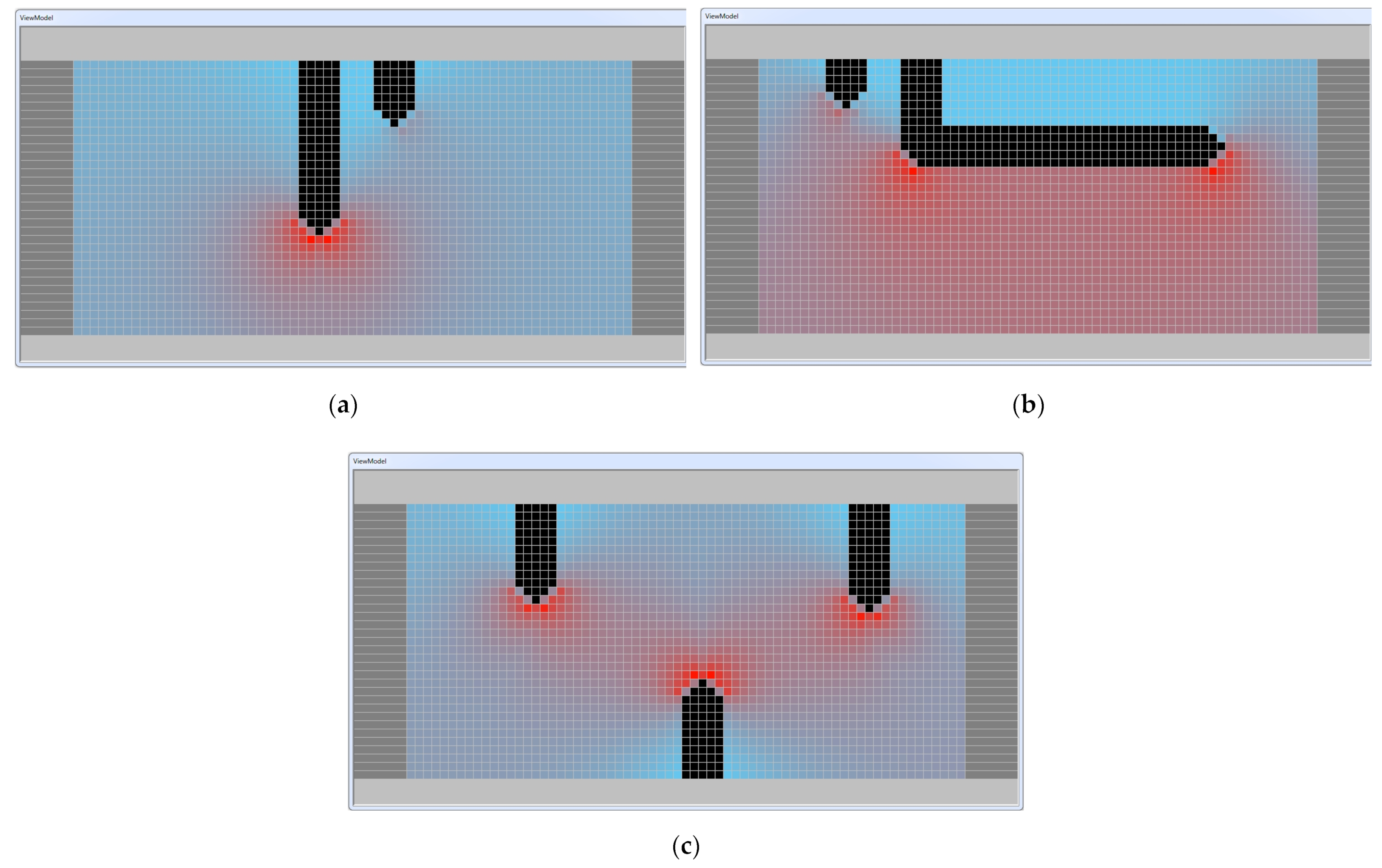
Let us consider the general and detailed current and power distributions over the ERs of the simulation model (over the circuit branches). Figure 9 and Figure 10 show the trimmed resistor models with gradient fills.
The current is close to zero in the areas of the resistive film adjacent to the trim cut starting points. The path corners, where the laser beam changes its direction, envelope the converging current lines. It results in high currents and powers at the adjacent ERs.
For the I-cut (Figure 9a), the so-called “hot spot” is at the end of the path. For this path, the current power at the branches is the highest among all the other cut types. The L-, J-, U-, and S-cuts (Figure 9b–e) have two hot spots at each of the path corners. The resistive film segment adjacent to the second leg of the paths is slightly less loaded. This is because the current lines coming from the trimmed contact area of the conductive and resistive layers and going around the cut path corners are redistributed across the remaining width of the resistor.
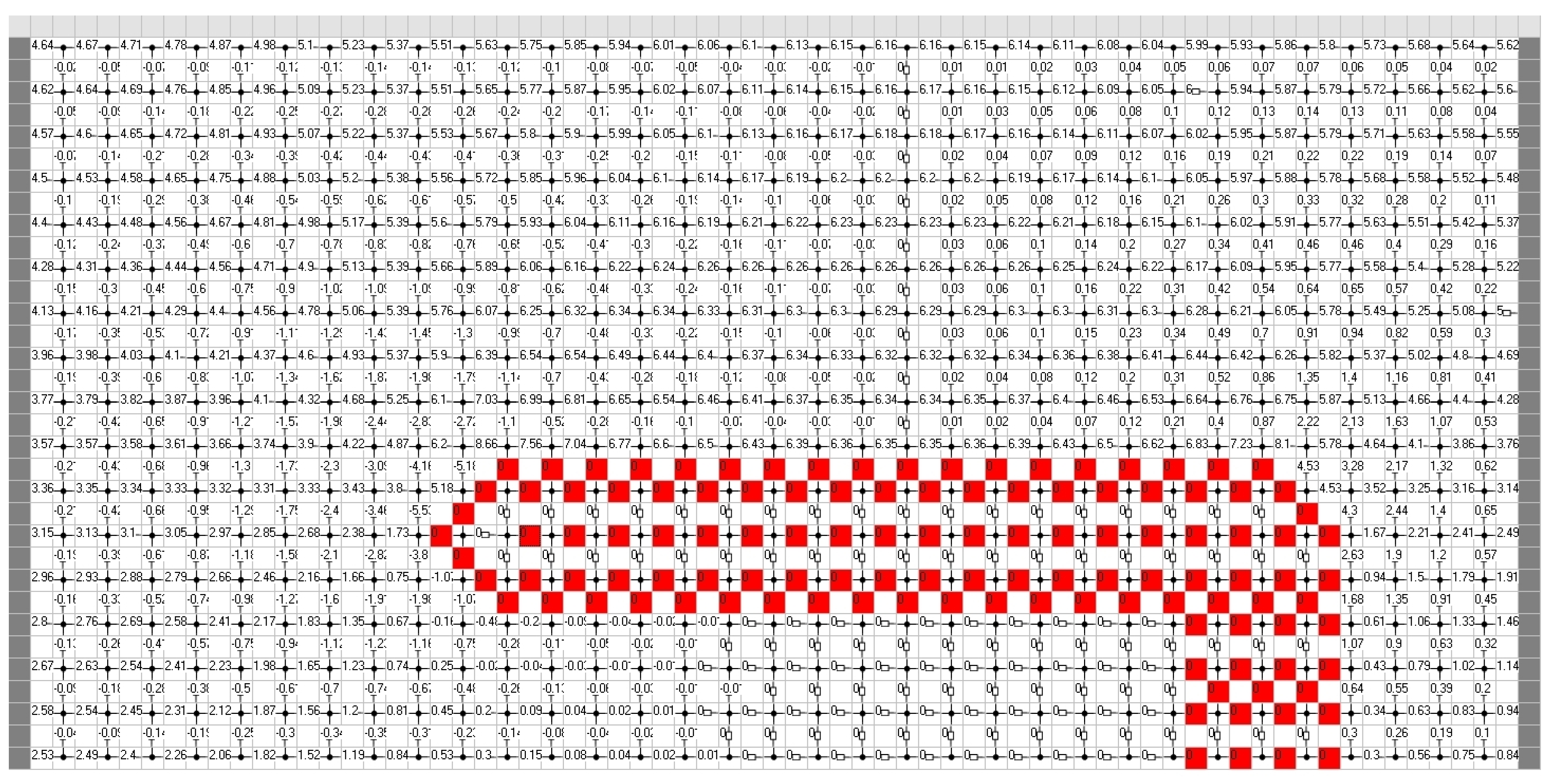
Let us now simulate the L-cut trim with the parameters listed in Table 9 except for the node size: it is set to 12 μm instead of 6 μm. The initial current distribution across the ERs is shown in Figure 11. The current passing through the horizontal ERs is the same and approximately equal to 0.368 mA (for clarity, the displayed current values in this example are multiplied by 10). There is no current passing through the vertically oriented resistors. After the trim, the current lines are distorted around the path corners and tend to be evenly distributed over the area between the second leg of the cut and the edge of the resistor (see Figure 12). The arrows show the current directions. The currents at the grid branches are shown in Figure 13.
The distribution of currents shows that the current at the ERs adjacent to the path corners is more than 100% higher than the original values for this example. Additionally, note the section of the resistor below the L-cut. Figure 12 and Figure 13 show that the resistive film segment under the second leg of the path also acts as a resistor, and the currents on the branches of this segment are rather significant.
Table 10 summarizes the ResModel simulation results (Figure 8, Figure 9 and Figure 10).

6. Discussion

The resistor trim curves produced by ResModel agree well with [5,6,23,27,33,34,36]. The “hot spot” locations at the laser cut path and the current directions also correlate very well with [18,20,27,36]. The current load distributions presented in [5,6,22,33] are slightly different. We believe this is due to the visualization features of the specific simulator, not to any errors in the models.
The ResModel software not only verifies the models and algorithms for estimating the electrophysical parameters of resistive medium (thin film, thick film, or foil) but is also a valuable tool for studying the relationships between the resistor configuration and its performance such as the max power dissipation, resistance drift over time, etc. The proposed approaches to simulation allow us to calculate the final resistance after a certain trim and to investigate the distribution of current, voltage, and power over the ERs. In the future, this will enable the specification of the criteria important for resistor operation such as:
  • Min number of hot spots;
  • Min length of the trim path and min HAZ where the current load is greater than a specified share of the initial current load;
  • Max acceptable power dissipation.
The above software features are extremely important to embed the proposed models and algorithms in industrial laser equipment for resistor trimming. The models are very versatile in terms of simulating resistors and trims of various configurations beyond those discussed in this paper.
In general, we consider the combination of the following factors to be the main novelty of the software developed and presented in this work. Firstly, this system has a wide functionality: calculating the resistance value for various types of trimming cuts and for various configurations of resistive elements, searching for optimal trimming trajectories according to one or another criterion, building trimming curves, determining the current load and power dissipation in any of the sections of the resistive conductive environment. Secondly, the ResModel software is a specialized tool for modeling the process of trimming film and foil resistors; this allows the use of computing tools tuned specifically to solve such problems, which provides a significant increase in speed and much higher visibility. Additionally, thirdly (and most importantly), despite the complete autonomy and independence of the developed software, its final purpose is to be integrated into the control system of industrial laser equipment for adjusting film and foil resistors. Indeed, if the user sets all the initial data for modeling (Table 3 in the article under consideration) manually when used independently, then when embedded in a real control system, part of the data (geometrical dimensions of the resistor, diameter, and location of the laser radiation spot) will be received by the system using the optical system of the installation and machine vision algorithms, and the other part with the help of measuring instruments (ohmmeter or other measuring system).
We should also mention such critical characteristics of any simulation model as accuracy and performance [53]. For a complete analysis of these characteristics, it will be advisable to simulate identical resistors in different software packages (dedicated and general purpose). The resistance simulation results should be compared to the resistance of actual trim resistors formed of various resistive materials and in the commonly used configurations. Such a model verification is highly relevant to meet the chip miniaturization and process automation trends. The next and final publication in this series will cover these criteria in detail.
7. Conclusions

We developed the ResModel simulation software based on the previously presented grid models of the resistor laser trimming.
As to the further development of this field in general and the ResModel software in particular, it should be noted that the currently available electrophysical properties of resistors are for DC only. However, a significant number of resistors are used in HF and UHF circuits. They are attenuators, power dividers, converters, and loads. Additional characteristics, such as capacitance and inductance, power dissipation under pulse load, etc. [54,55], should be studied. The extra functionality requires new calculation algorithms and visualization tools. The introduction of such functions first in the ResModel software and then in the industrial controllers will enable the selection of an optimal laser trim path for adjusting not only the resistance of individual resistors, but also for the optimization of such parameters as frequency, the amplitude of the AC signal, or complex interference. Moreover, trimming removes some cost-related issues discussed in [56].
We believe the detailed description of the simulation model building and the trim control algorithm is a significant advantage of this study in particular and the cycle of papers. The authors hope that this work and further research of the model as part of a simulation system and an industrial laser trimming machine will invite other researchers to discuss and explore this area in depth.

Author Contributions

Conceptualization, V.V.K. and V.V.C.; methodology, V.V.K.; validation, O.S.S.; investigation, V.V.K., V.V.C., O.S.S., E.V.Z. and I.K.T.; writing (original draft), V.V.K.; writing (review and editing), V.V.K., O.S.S., E.V.Z. and I.K.T.; supervision, V.V.K.; funding, E.V.Z. and I.K.T. All authors have read and agreed to the published version of the manuscript.

Funding

The research is partially funded by the Ministry of Science and Higher Education of the Russian Federation as part of the World-Class Research Center program: Advanced Digital Technologies (contract No. 075-15-2022-312 dated 20.04.2022).

Data Availability Statement

Not applicable.

Conflicts of Interest

The authors declare no conflict of interest.

Appendix A

Figure A1. The system matrix for the example given in Section 3.
Electronics 12 00589 g0a1

References

  1. Denisenko, V.V. Computer Control of Technological Process, Experiment, Equipment; Hotline-Telecom Publishers: Moscow, Russia, 2011; p. 606. (In Russian) [Google Scholar]
  2. Kondrashov, V.V.; Chapkin, V.V.; Lukashenkov, A.V. Circuit simulation of the process of film resistive elements laser trimming under the effect of a measuring current source. J. Phys. Conf. Ser. 2018, 1109, 012012. [Google Scholar] [CrossRef]
  3. Kondrashov, V.V.; Chapkin, V.V.; Seredin, O.S.; Zemlyakov, E.V.; Pozdeeva, E.Y. Circuit Simulation of Film Resistor Laser Trimming with a Measuring Voltage Source. Electronics 2022, 11, 767. [Google Scholar] [CrossRef]
  4. Tam, W.S.; Kok, C.W. Tutorial on Resistor Trimming. Solid State Electron. Lett. 2021, 3, 11–18. [Google Scholar] [CrossRef]
  5. Sandborn, P.; Sandborn, P. Using embedded resistor emulation and trimming to demonstrate measurement methods and associated engineering model development. Int. J. Eng. Educ. 2007, 23, 834. [Google Scholar]
  6. Sandborn, P. A Random Trimming Approach for Obtaining High-Precision Embedded Resistors. IEEE Trans. Adv. Packag. 2008, 31, 76–81. [Google Scholar] [CrossRef]
  7. Sadkov, V.D.; Pilkevich, A.V.; Fomina, K.S. Modeling of the Laser Trimming Process of the Film Absorbing Elements. Nano-I Mikrosist. Tekhnika 2018, 20, 402–408. (In Russian) [Google Scholar] [CrossRef]
  8. Korshunova, E.N.; Sadkov, V.D. Process modeling of laser trimming of resistance of the film resistor. In Proceedings of the XXIV International Scientific and Technical Conference, Nizhny Novgorod, Russia, 20 April 2018; pp. 117–121. (In Russian). [Google Scholar]
  9. Pilkevich, A.V.; Sadkov, V.D. Mathematical Apparatus for Modeling Passive Elements of Integrated Circuits. In Proceedings of the XXVII International Conference, Nizhny Novgorod, Russia, 23–24 April 2021; pp. 1023–1027. (In Russian). [Google Scholar]
  10. Pilkevich, A.V.; Fomina, K.S.; Sadkov, V.D. Modeling of process of laser matching of the film absorbing elements in ELCUT. In Proceedings of the XXIV International Scientific and Technical Conference, Nizhny Novgorod, Russia, 20 April 2018; pp. 154–159. (In Russian). [Google Scholar]
  11. ELCUT—Simulation Program. Available online: http://elcut.ru/index.htm (accessed on 1 December 2022).
  12. Walton, A.; Holwill, R.; Robertson, J. Numerical simulation of resistive interconnects for integrated circuits. IEEE J. Solid-State Circuits 1985, 20, 1252–1258. [Google Scholar] [CrossRef]
  13. Horowitz, M.; Dutton, R. Resistance Extraction from Mask Layout Data. Computer-Aided Design of Integrated Circuits and Systems. IEEE Trans. Comput. Aided Des. Integr. Circuits Syst. 1983, 2, 145–150. [Google Scholar] [CrossRef]
  14. Van der Woerd, A.C.; van Lammeren, J.P.M.; Janse, R.J.H.; van Beynhem, R.H. Calculation of the resistance value of laser-trimmable planar resistors in an interactive mask-layout design system. IEEE J. Solid-State Circuits 1984, 19, 532–537. [Google Scholar] [CrossRef]
  15. Rubanovich, M.G.; Aleksandrov, N.V.; Manusov, V.Z.; Khrustalyov, V.A. Electromagnetic simulation of film resistor. Proc. Tomsk. State Univ. Control. Syst. Radioelectron. 2013, 3, 63–70. (In Russian) [Google Scholar]
  16. Mueller, M.; Mickanin, W. Functional Laser Trimming of Thin Film Resistors on Silicon ICs. In Proceedings of the SPIE 0611, Laser Processing of Semiconductors & Hybrids, Los Angeles, CA, USA, 21–22 January 1986. [Google Scholar] [CrossRef]
  17. Mitsuhashi, T.; Yoshida, K. A Resistance Calculation Algorithm and Its Application to Circuit Extraction. IEEE Trans. Comput. -Aided Des. Integr. Circuits Syst. 1987, 6, 337–345. [Google Scholar] [CrossRef]
  18. Ramirez-Angulo, J.; Geiger, R.; Sanchez-Sinencio, E. Characterization, Evaluation, and Comparison of Laser-Trimmed Film Resistors. Solid State Circuits IEEE J. Solid-State Circuits 1988, 22, 1177–1189. [Google Scholar] [CrossRef]
  19. Ramirez-Angulo, J.; Wang, R.; Geiger, R. Improvement of laser trimmed film resistor stability by selection of optimal trim paths. IEEE Int. Sympoisum. Circuits Syst. 1991, 4, 2188–2191. [Google Scholar]
  20. Ramirez-Angulo, J.; Geiger, R. New laser-trimmed film resistor structures for very high stability requirements. IEEE Trans. Electron. Devices 1988, 35, 516–518. [Google Scholar] [CrossRef]
  21. Shier, J. A finite-mesh technique for laser trimming of thin-film resistors. IEEE J. Solid-State Circuits 1988, 23, 1005–1009. [Google Scholar] [CrossRef]
  22. Papp, G.M. Simulation of Laser Trimming of Film Resistors. Period. Polytech. Electr. Eng. 1993, 37, 43–52. [Google Scholar]
  23. Moran, P.; Maiti, C. A Program to Predict the Resistance of Trimmed Film Resistors. Act. Passiv. Electron. Components. Hindawi Publ. Corp. 1976, 3, 153–164. [Google Scholar] [CrossRef] [Green Version]
  24. Schimmanz, K.; Kost, A. BEM Simulation of Laser Trimmed Hybrid IC Resistors. Int. J. Appl. Electromagn. Mech. 2004, 19, 253–256. [Google Scholar] [CrossRef] [Green Version]
  25. Schimmanz, K.; Kost, A. Formulation of mixed elements for the 2D-BEM. COMPEL Int. J. Comput. Maths. Electr. Electron. Eng. 2004, 23, 866–875. [Google Scholar] [CrossRef]
  26. Schimmanz, K.; Jacobsen, S.M. Resistance Post-Trim Drift Index for Film Resistors to Be Trimmed; Preprint BTU-Cottbus M-01/02; BTU: Cottbus, Germany, 2002. [Google Scholar]
  27. Schimmanz, K.; Jacobsen, S.M. Film Resistor Design for High Precision Laser Trimming; Preprint BTU-Cottbus M-02/02. Available online: http://resistor.vitr.org/rdesign.pdf (accessed on 1 December 2022).
  28. RCutSim—Simulation Program. Available online: http://resistor.vitr.org/ (accessed on 1 December 2022).
  29. Qinfang, X.; Shiyu, L.; Meizhi, R. Resistance calculation from geometric layout data by boundary element method. In International Conference on Circuits and Systems. In Proceedings of the 1991 International Conference on Circuits and Systems, Shenzhen, China, 16–17 June 1991; pp. 863–866. [Google Scholar] [CrossRef]
  30. Hulong, Z.; Jie, Z. Analytical Solution of Chip Resistor’s Trimming Behavior. In Proceedings of the 36th Youth Academic Annual Conference of Chinese Association of Automation (YAC), Nanchang, China, 28–30 May 2021; pp. 632–636. [Google Scholar] [CrossRef]
  31. Hall, P.M. Resistance calculations for thin film patterns. Thin Solid Films 1968, 1, 277–295. [Google Scholar] [CrossRef]
  32. Chawla, B.R.; Gummel, H.K. A boundary technique for calculation of distributed resistance. IEEE Trans. Electron Devices 1970, 17, 915–925. [Google Scholar] [CrossRef]
  33. Kaminski, S.; Mis, E.; Szymendera, M.; Dziedzic, A. New Trim Configurations for Laser Trimmed Thick-Film Resistors—Experimental Verification. IMAPS J. Microelectron. Electron. Packag. 2005, 2, 19–24. [Google Scholar] [CrossRef]
  34. Wroński, M.; Kamiński, S.; Miś, E.; Dziedzic, A. New trim configurations for laser trimmed thick-film resistors—Theoretical analysis, numerical simulation and experimental verification. Microelectron. Reliab. 2005, 45, 1941–1948. [Google Scholar] [CrossRef]
  35. Laser Systems—Aurel Automation. Available online: https://www.aurelautomation.com/laser-systems/ (accessed on 1 December 2022).
  36. Manolescu, A.; Manolescu, A.M. Laser Trimming Modeling of Thin Film Integrated Resistors. In Proceedings of the International Semiconductor Conference, CAS 2007, Sinaia, Romania, 15–17 October 2007; pp. 473–476. [Google Scholar] [CrossRef]
  37. Birkett, M.; Penlington, R. Laser Trim Pattern Optimization for CuAlMo Thin-Film Resistors. IEEE Trans. Compon. Packag. Manuf. Technol. 2013, 3, 523–529. [Google Scholar] [CrossRef]
  38. Alafogianni, M.; Penlington, R.; Birkett, M. Resistor trimming geometry; past, present and future. IOP Conf. Ser. Mater. Sci. Eng. 2016, 104, 012002. [Google Scholar] [CrossRef] [Green Version]
  39. Antonov, Y. Features of application of the laser method for normalization of accuracy of resistors in hybrid integrated circuits. Key Eng. Mater. 2005, 291–292, 643–646. [Google Scholar] [CrossRef]
  40. Lasers and Apparatus. Available online: https://laserapr.ru/category/podgonka-rezistivnyh-elementov/ (accessed on 1 December 2022).
  41. Josef, S.; Kolarik, J.; Szendiuch, I. Prediction of the Thick Film Resistor Trimming. 2017. Available online: https://www.semanticscholar.org/paper/PREDICTION-OF-THE-THICK-FILM-RESISTOR-TRIMMING-Sk%C3%A1cel-Kolarik/0a3f47817ecc496e38752a4023b3422304c46ac5/ (accessed on 1 December 2022).
  42. Antonov, Y.N. Application of Computer Graphics to Resistor Laser Trimming. In Proceedings of the International Conference on Microelectronics in Mechanical Engineering, Ulyanovsk, Russia, 11–12 March 1992; pp. 39–40. (In Russian). [Google Scholar]
  43. Gantmacher, F.R. Matrix Theory; Nauka: Moscow, Russia, 1988; p. 552. (In Russian) [Google Scholar]
  44. Kharchenko, S.A. Parallel Iterative Algorithm for Solving Asymmetric Systems of Linear Equations with Partial Preservation of Spectral/Singular Information and Explicit Restarts. Comput. Methods Program. 2010, 11, 373–381. [Google Scholar]
  45. Greenbaum, A. Iterative Methods for Solving Linear Systems; Society for Industrial and Applied Mathematics (SIAM): Philadelphia, PA, USA, 1997. [Google Scholar] [CrossRef] [Green Version]
  46. Golub, G.H.; van Loan, C.F. Matrix Computations, 3rd ed.; John Hopkins University Press: London, UK, 1996; p. 687. [Google Scholar]
  47. Lukas, J.R. Matrix Analysis of Networks. Available online: http://prof.rohan.lucas.lk/images/notes/ENotes/EE201_matrix_analysis.pdf (accessed on 1 December 2022).
  48. Chua, L.O.; Pen-Min, L. Computer-Aided Analysis of Electronic Circuits: Algorythms and Calculation Methods; Translated from English; Energiya Publishers: Moscow, Russia, 1980; p. 640. (In Russian) [Google Scholar]
  49. Tewarson, R.P. Sparce Matrices; Academic Press, Inc.: New York, NY, USA, 1973. [Google Scholar]
  50. Ross, D.J.; Willoughby, R.A. Sparce Matrices and Their Applications; Plenum Press: New York, NY, USA, 1972. [Google Scholar]
  51. Mouton, C. Linear Algebra Libraries. Available online: https://www.academia.edu/26346676/Linear_Algebra_Libraries (accessed on 1 December 2022).
  52. Eigen. Available online: http://eigen.tuxfamily.org/index.php?title=Main_Page (accessed on 1 December 2022).
  53. Mourtzis, D. Simulation in the design and operation of manufacturing systems: State of the art and new trends. Int. J. Prod. Res. 2019, 58, 1927–1949. [Google Scholar] [CrossRef]
  54. Mitkov, A.S.; Razinkin, V.P.; Khrustalyov, V.A. Increasing the Input Power in Multielement Microwave Film Attenuators. Proc. Russ. High. Educ. Acad. 2021, 3, 32–43. [Google Scholar] [CrossRef]
  55. Pilkevich, A.V.; Sadkov, V.D. Thin Film Absorbing Elements for GIS Embedded Attenuators. Univ. Bulletin. Electron. 2021, 26, 521–532. [Google Scholar] [CrossRef]
  56. Sandborn, P. An assessment of the applicability of embedded resistor trimming and rework. IEEE Trans. Electron. Packag. Manuf. 2005, 28, 176–186. [Google Scholar] [CrossRef] [Green Version]
Figure 1. ResModel simulation software. Main window.
Electronics 12 00589 g001
Figure 2. General view of the resistor simulation model.
Electronics 12 00589 g002
Figure 3. Detailed view of the resistor simulation model.
Electronics 12 00589 g003
Figure 4. Example: laser spot visualization.
Electronics 12 00589 g004
Figure 5. General view of the simulated resistor with a gradient fill.
Electronics 12 00589 g005
Figure 6. Simple trims.
Electronics 12 00589 g006
Figure 7. Composite trim configurations.
Electronics 12 00589 g007
Figure 8. Resistor trimming curves for the trim types studied. The figure shows the RTCs for the following trim types: (a) I-cut; (b) L-cut; (c) J-cut; (d) U-cut; (e) S-cut; (f) Ii-cut; (g) Li-cut; (h) W-cut.
Electronics 12 00589 g008aElectronics 12 00589 g008b
Figure 9. Current distribution for simple cut types represented as a gradient fill: (a) I-cut; (b) L-cut; (c) J-cut; (d) U-cut; (e) S-cut.
Electronics 12 00589 g009
Figure 10. Current distribution for composite cut types represented as a gradient fill: (a) Ii-cut; (b) Li-cut; (c) W-cut.
Electronics 12 00589 g010
Figure 11. Initial distribution of currents over the ERs.
Electronics 12 00589 g011
Figure 12. Current directions over the grid branches after a laser trim.
Electronics 12 00589 g012
Figure 13. Distribution of currents over the grid branches after a laser trim.
Electronics 12 00589 g013
Table 1. Model variables.
NameData TypeDescription
Geometry
ResLintegerResistor length, μm
ResHintegerResistor width, μm
DintegerLaser spot diameter, μm
NodeSizeintegerNode size, μm
NodeRowCountintegerNumber of grid rows
NodeColCountintegerNumber of grid columns
NodeCountintegerTotal number of grid nodes
BranchCountintegerTotal number of ER
scXintegerLaser spot coordinates, µm
scYinteger
Electrophysical parameters
RPreTestsinglePretest resistance, Ohm
RNomsingleRated resistance, Ohm
RmsinglePredicted resistance, Ohm
EmsinglePredicted resistance deviation from the rated value, %
r1singleER resistance, Ohm
IcsingleCurrent of the measurement source, mA
Table 2. Data arrays.
NameData TypeMatrix SizeDescription
ArrAShortInt ( N o d e C o u n t + 1 )
×
( B r a n c h C o u n t + 1 )
A 0 reduced incidence matrix (subsection (3) in [2])
Arr1Integer 1 + 2 ( N o d e R o w C o u n t 1 )
×
1 + 2 N o d e C o l C o u n t
Matrix representing the grid model and intermediate operations
Arr2BrInteger 1 + 2 ( N o d e R o w C o u n t 1 )
×
1 + 2 N o d e C o l C o u n t
Branch matrix
Arr3NodeInteger N o d e R o w C o u n t
×
N o d e C o l C o u n t
Node matrix
Arr3NodeISingle N o d e R o w C o u n t
×
N o d e C o l C o u n t
Node matrix containing the sum of the absolute current values on the branches adjacent to the node
ArrSShortInt ( N o d e C o u n t + 1 )
×
( N o d e C o u n t + 1 )
Y N system matrix (reduced nodal conductivity matrix) (Equation (11) in [2])
Grand- Arr3NodeInteger N o d e R o w C o u n t
×
N o d e C o l C o u n t
×
M o d e l C o u n t
Set of two-dimensional matrices containing the “image” of the resistor with a particular trim path, ModelCount: the number of such “images”
VUnReal ( N o d e C o u n t + 1 ) × 1 Voltage column vector at the u N nodes (Equation (9) in [2])
VUrSingle ( B r a n c h C o u n t + 1 ) × 1 Voltage vector column at the u B ERs (Equation (5) in [2])
VISingle ( B r a n c h C o u n t + 1 ) × 1 Column vector containing the current values at the i B branches
VPSingle ( B r a n c h C o u n t + 1 ) × 1 One-dimensional array containing the power values on the P branches
vCBIntegerOne-dimensional array of arbitrary lengthStores the numbers of cut branches and resistance values obtained through trim simulation
vRSingle
GrandVRSingle M o d e l C o u n t of vR one-dimensional arraysSet of vectors containing the resistance values of the ER “images” from the GrandArr3Node arrays
Table 3. Input data for trim simulation.
PropertyValue
Resistor length L, μm300
Resistor width H, μm200
Laser spot diameter D, μm25
Node size, µm25
Pretest resistance, Ohm100
Resistor rating, Ohm150
Rated error, %±0.5
Measuring current, mA2.5
Table 4. Basic resistor model properties.
PropertyDesignationValue
Resistor length, μmResL300
Resistor width, μmResH200
Laser spot diameter, μmD25
Node size, μmNodeSize25
Number of grid rowsNodeRowCount8
Number of grid columnsNodeColCount12
Total number of grid nodesNodeCount97
Total number of ERBranchCount188
Predicted resistance, OhmRm140.317
Predicted resistance deviation from the rated value, %Em−6.455
Resistance, Ohmr161.538
Size of the reduced incidence matrixArrA98 × 189
Size of the matrix containing the grid model and intermediate operationsArr112 × 25
Size of the branch matrixArr2Br12 × 25
Size of the node matrixArr3Node8 × 12
Size of the node matrix containing the absolute values of currents at the resistors adjacent to the nodeArr3NodeI8 × 12
Size of the array containing the Y N system matrixArrS98 × 98
Size of the vector column containing voltages at u N nodesVUn98 × 1
Size of the vector column containing voltages at the u B resistorsVUr188 × 1
Size of the vector column containing the currents at the i B branchesVI188 × 1
Size of the array containing the power values at the P branchesVP188 × 1
Table 5. Arr1 array contents.
11190170251331411491571651731811891
0101010101010101010101010
121100180261341421501581661741821901
0101000000000001010101010
131110191271351431510591671751831911
0101000000000001010101010
141121201281361441521601681761841921
0101010101010101010101010
151131211291371451531611691771851931
0101010101010101010101010
161141221301381461541621701781861941
0101010101010101010101010
171151231311391471551631711791871951
0101010101010101010101010
181161241321401481561641721801881961
Table 6. Arr2Br array contents.
1016031046061076091010601210136015101660181
09024039054069084099011401290144015901740
2017032047062077092010701220137015201670182
0100250400550700850100011501300145016001750
3018033048063078093010801230138015301680183
0110260410560710860101011601310146016101760
4019034049064079094010901240139015401690184
0120270420570720870102011701320147016201770
5020035050065080095011001250140015501700185
0130280430580730880103011801330148016301780
6021036051066081096011101260141015601710186
0140290440590740890104011901340149016401790
7022037052067082097011201270142015701720187
0150300450600750900105012001350150016501800
8023038053068083098011301280143015801730188
Table 7. Arr3Node array contents.
110111111111
110111111111
110000011111
111111111111
111111111111
111111111111
111111111111
111111111111
Table 8. Arr3NodeI array contents.
0.37330.240300.00180.00730.02750.10280.38370.62640.79090.88790.9323
0.50630.58800.00180.00730.02750.10280.80550.70470.85840.94050.9767
0.7981.2319000001.50710.91220.99751.03911.0572
1.43022.20092.20092.04572.01632.10152.33352.33351.47231.24521.18011.161
1.63231.89481.93551.94021.94671.95471.95471.91961.60891.41611.31691.269
1.70141.81051.86131.8781.8781.87561.85111.78131.62761.49351.40221.3485
1.73021.78461.82111.83481.83481.82641.79291.72681.62681.52791.45011.3987
1.74141.77661.80381.81371.81371.80241.76721.70631.62481.54141.47141.4228
Table 9. Input data for trim simulation.
PropertyValue
Resistor length L, μm400
Resistor width H, μm200
Laser spot diameter D, μm24
Node size NS, μm6
Pretest resistance, Ohm100
Resistor rating, Ohm150
Rated error, %±1
Measuring current, mA2.5
Table 10. ResModel trim simulation results.
Type of Cut
PropertyILJUSIiLiW
Number of steps along the trim legs2112 + 4412 + 44 + 312 + 44 + 952821 + 813 + 34 + 612 + 12 + 13
Total number of steps21565965528295337
Final resistance, Ohm148.903149.748149.803149.812149.812150.007149.926150.576
Error, %−0.731−0.168−0.131−0.125−0.1250.004−0.050.384
Highest branch current, mA0.8940.4290.4270.4270.4270.8910.4520.684
Disclaimer/Publisher’s Note: The statements, opinions and data contained in all publications are solely those of the individual author(s) and contributor(s) and not of MDPI and/or the editor(s). MDPI and/or the editor(s) disclaim responsibility for any injury to people or property resulting from any ideas, methods, instructions or products referred to in the content.