1. Introduction
Layout-dependent effects (LDEs) in advanced manufacturing processes are having an increasing effect on integrated circuit (IC) design. IC quality improvements and optimization are often achieved through an iterative process involving presimulations and postsimulations, especially for low-power, high-frequency circuits. However, presimulations and postsimulation often differ greatly for IC designs for advanced semiconductor processes, leading to long design iteration cycles. Therefore, many foundries provide IC designers with process design kits (PDKs) for analog/mixed-signal design and verification, reducing the length of design iteration cycles [
1].
Semiconductor processes are evolving, and design for manufacturability (DFM) must now be incorporated into the IC design flow. During the implantation of dopants to form wells for metal–oxide semiconductor (MOS) transistors, thermal resistors are patterned outside of these areas to prevent unwanted ion penetration. Ions that strike near the edge of the photoresist may backscatter and become embedded in the silicon adjacent to the edge of the photoresist. This leads to the well doping being nonuniform across the wafer, resulting in device wells near the edge having a greater V
TH (threshold voltage). This phenomenon is called the well proximity effect (WPE). As transistor feature sizes decrease, stress-induced variation has also become an unavoidable problem. Unintentional stress, such as that caused by shallow trench isolation (STI), is a primary source of variation and is closely related to layout. STI stress causes changes in mobility, V
TH, and saturation velocity. This is known as a length of diffusion (LOD) effect; the characteristics of a device vary with the distance of its gate from the diffusion edge. The WPE and LOD effect are two factors that are often considered in DFM [
2].
Foundries typically provide design rules and parameters for individual components. For example, PDKs only provide information regarding a single device instance required for an IC’s design and layout; PDKs do not consider the impact of regional DFM on the overall IC layout. Although the PDK setting in [
3] included the WPE and LOD, this setting also affected the layout structure of one or a few components. Because LDEs affect DFM, completely eliminating the differences between the presimulation and postsimulation results with only a PDK is impossible. Therefore, to design high-precision, high-performance circuits, using an automation program to extract the DFM parameters of the overall regional device in advance is critical for enabling IC designers to analyze the effects of MOS group matching on DFM. Moreover, although size matching greatly affects electrical performance and characteristics, V
TH matching is also critical for performance. If the DFM parameters of the overall regional device can be extracted in advance, the design iteration cycle can be greatly shortened.
Proposed Methodology
- A.
WPE and LOD Effect
The WPE results in higher V
TH values for devices near the well edge than for general devices. The effect of the spacing from the edge of the well to the edge of the device on the V
TH variation due to WPE was modeled. The V
TH VT0 can be modeled as follows:
where V
T0,noWPE is the
VT0 without WPE;
KVT0WE,
WEB, and
WEC are fitting parameters; and the quantities
SCA,
SCB, and
SCC depend on the layout geometries of the transistor and the well edges. Increasing SCA, SCB, and SCC increases
VT0. SCA, SCB, and SCC are calculated as follows:
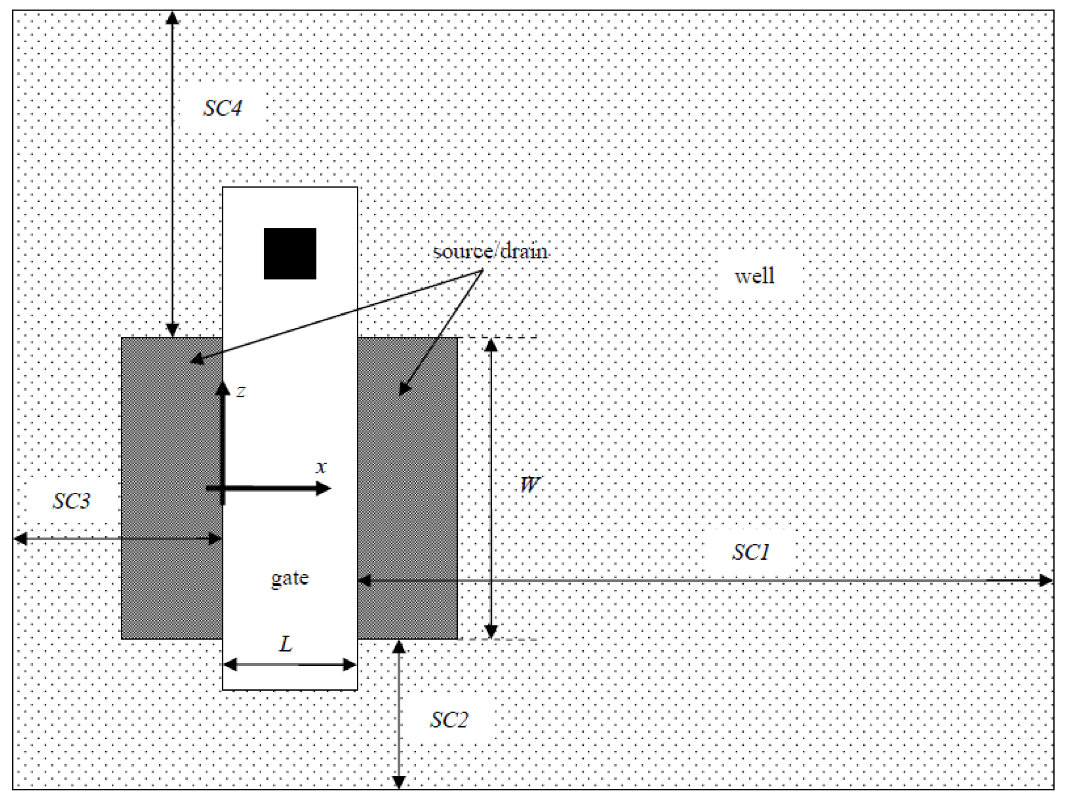
where SC1–SC4 are the spacings from the four edges of the well to the edges of the device as shown in
Figure 1. Equations (1)–(4) show that
VT0 depends on the spacing from the edge of the well to the edge of the device.
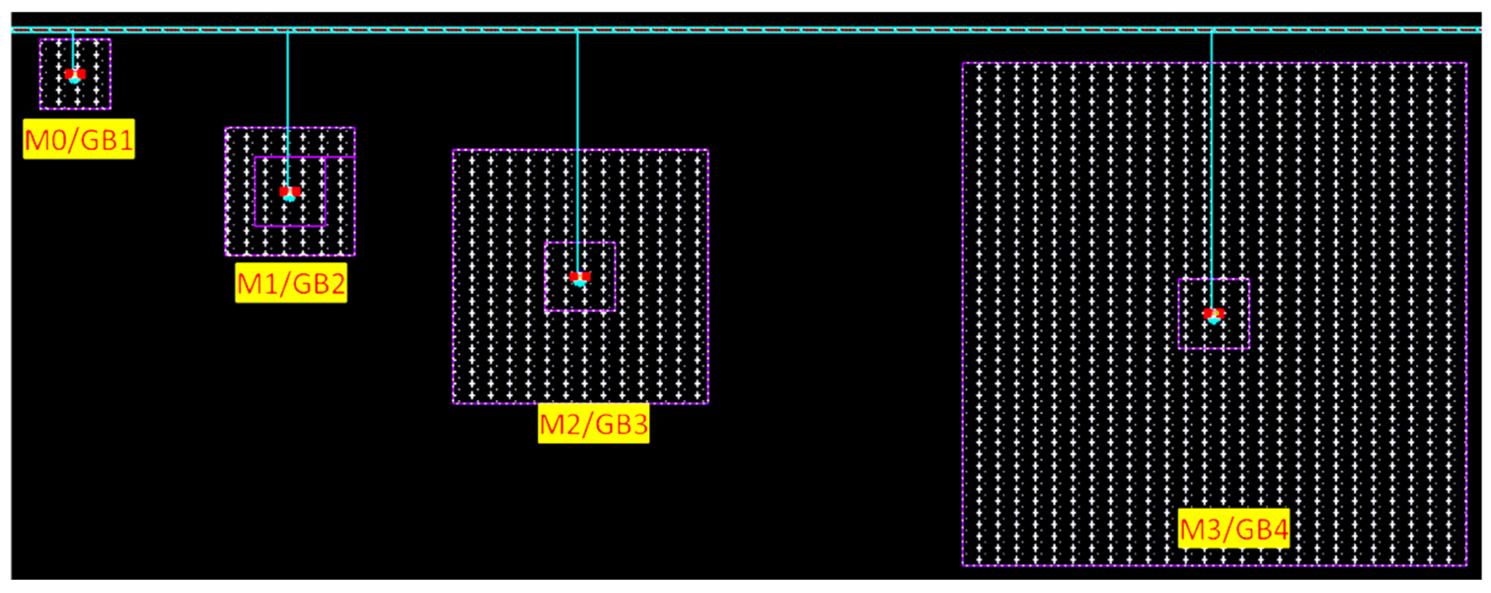
As shown in
Figure 2, four MOS transistor layouts of different sizes—labeled M0, M1, M2, and M3—were generated from a foundry standard PDK library to investigate DFM. The spacing between the well edge and the oxide edge of M0, M1, M2, and M3 is 2.6, 5, 10, and 20 μm, respectively. Once LVS (layout versus schematic) had been completed, Siemens EDA Caliber XRC software was used to perform layout parasitic extraction (LPE) flow with the 28-nm LPE command file provided by the foundry.
Table 1 shows the LPE results. The extracted SCA, SCB, and SCC values of M0 are much larger than those of M1, M2, and M3, indicating that the WPE is greater on a MOS transistor with a smaller spacing between the well edge and the device oxide edge. The SCA, SCB, and SCC values of M1 are smaller than those of M0 but larger than those of M2 and M3, indicating that the WPE becomes weaker as the spacing between the well edge and the device oxide edge is increased, but the WPE can be neglected when the spacing between the well edge and the device oxide edge is larger than 10 μm. As revealed by the extracted parameters presented in
Table 1 and obtained from Equations (1)–(4), a smaller spacing between the well edge and the device oxide edge is associated with larger values of SCA, SCB, SCC, and V
TH.
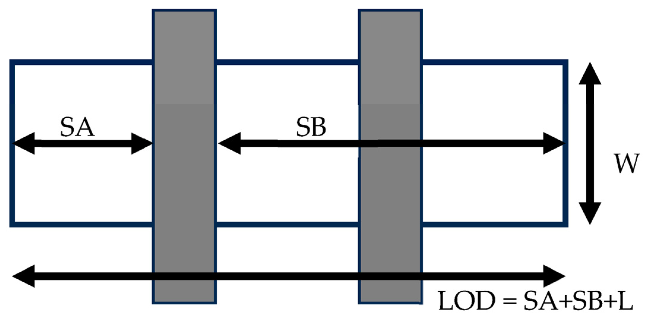
Figure 3 presents a typical MOSFET layout. The layout parameters of interest are listed in the figure.
W and
L represent the gate’s width and length, respectively; SA and SB are lengths between each gate and the STI edge; and LOD is the length of the active area.
The equations in the BSIM4.6.1 MOSFET Model User’s Manual [
5] reveal that SA and SB are related to V
TH and should be maximized during design. Equation (5) indicates that the original V
TH (VTH0) is positively correlated with Inv_sa and Inv_sb, which are inversely correlated with SA and SB, respectively. Therefore, the stability of VTH0 is better when the SA and SB parameters obtained from the resistance and capacitance (RC) extraction tools are large than when they are small.
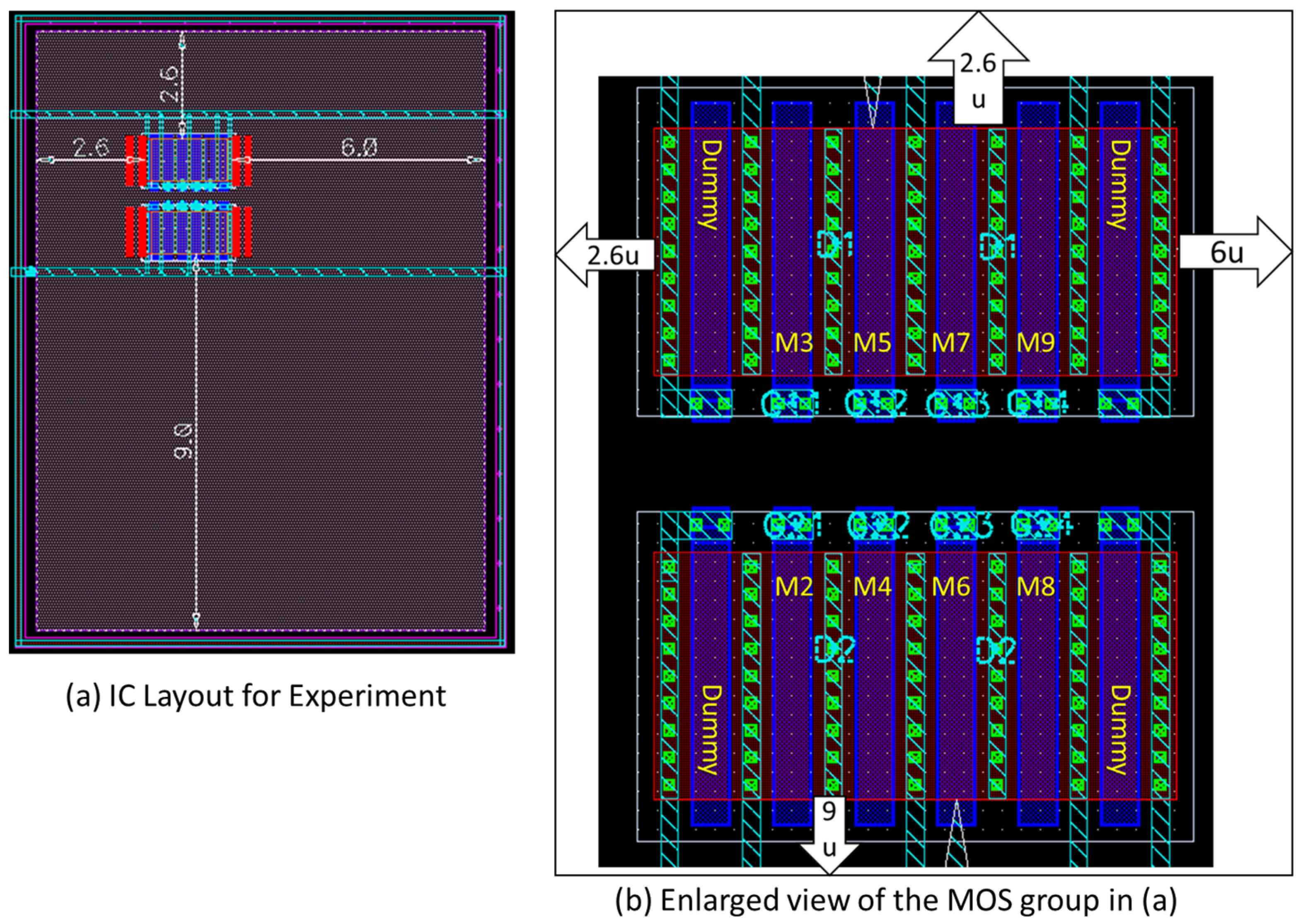
Figure 4 MOS layout obtained with DFM+Analog options enabled and using the PDK Library. The eight MOS components were created using the PDK library by selecting the DFM+Analog options. The number of fingers used in the layout was 6, and the leftmost and rightmost components were dummies. The spacings between the well edge and the top, bottom, left, and right oxide edges were 2.6, 9, 2.6, and 6 µm, respectively (
Figure 5). The DFM parameters extracted through LPE are displayed in
Table 2. The output results revealed that although the device design was based on the settings in the PDK library and conformed to relevant design rules, the eight components had different SA and SB values. Even when the dummy MOS components were considered, the effects of LOD on the SA and SB values varied (
Table 2). Consequently, the corresponding V
TH values also differed. Comparing the differences in SCA, SCB, and SCC revealed that the WPE also led to different V
TH values.
Examining these two IC layout examples indicates that even if layouts are created using the PDK cells provided by a foundry, the MOS components of the fabricated devices can still exhibit different VTH0/Idsat values because of variation in the device layouts. This leads to device mismatching and undermines circuit performance.
The proposed design process enables IC designers to determine the influence of DFM on circuit performance during the routing stage. Accordingly, designers can evaluate the effect of device placement on Vth0/Idsat and resolve any problems in advance. The subsequent postsimulation must address only the presence of the metal parasitic RC associated with device interconnection. This design method greatly reduces the necessary length of the design iteration cycle to achieve the strict matching requirements of low-energy-consumption and high-frequency ICs.
In reference [
8], it is indicated that CAD engineers have the potential to provide Process Design Kits (PDKs) to schematic designers of integrated circuits. While PDKs can anticipate layout proximity effects within schematics, accurate prediction of these effects is not feasible until the layout is finalized. The paper proposes a comprehensive e-DFM (electrical design for manufacturability) solution aimed at detecting, analyzing, and rectifying electrical hotspots (e-hots) arising from different process variations in simulated circuit designs. However, this method requires the prior collection of design intent to acquire all user-defined electrical constraints and contextual information regarding the actual physical layout, enabling the detection, analysis, and rectification of electrical hotspots.
This differs from the viewpoint presented in this paper, where we argue that designers can employ the standard RC-Extraction process provided by semiconductor foundries before the IC layout routing stage. This process enables the extraction of the most accurate physical parameters of components, such as AD, AS, PD, PS, as well as parameters related to WPE and LOD effects. At this stage, we can provide IC designers with a comprehensive Netlist containing all physical parameters of components and DFM (Design for Manufacturing) parameters. This Netlist, coupled with SPICE models, can offer IC designers the most accurate simulation analysis available before the IC layout routing phase.
2. Methods of a New Design Process
In reference [
1], Siemens EDA (formerly known as MENTOR GRAPHICS) mentioned the Process Design Kit (PDK) provided by semiconductor foundries, comprising schematic symbol libraries, parameterized layout cells (P-cells), Spice models, and relevant technical documentation. Utilizing PDK components offers advantages such as reducing the iteration count for Design Rule Checks (DRC). However, currently, there are no EDA tools capable of extracting component parasitic effects before the completion of IC layout routing and verification with Layout vs. Schematic (LVS).
Additionally, reference [
9] highlights that the primary functionality of IC layout tools revolves around drawing the physical IC layout. Although there exists the Schematic Driven Layout (SDL) feature, it merely facilitates the straightforward conversion of circuit elements from the schematic diagram to the IC layout without offering any Design for Manufacturing (DFM) effects or alerts to IC designers regarding DFM-related concerns. The IC design flow published by Cadence in reference [
6] also does not have the features proposed in this paper.
Reference [
10] discusses the continuous scaling down of CMOS technology. Advancements in lithography continually shrink the scale, intensifying interactions between adjacent patterns. Each pattern printed on a silicon wafer is affected by the interactions within a specific technological proximity to its neighboring patterns. The development of DFM-friendly standard cells, particularly for digital circuits, is of interest as mentioned in the paper. They propose a virtual characterization vehicle to address DFM issues for Standard Cells, which differs significantly from our proposed approach. Our new process is not restricted to any specific type of circuit, making it especially beneficial for analog IC design.
In the Introduction, the experimental outcomes depicted in
Figure 2 and
Figure 4 indicate that despite utilizing the PDK Cell provided by the foundry, differences persist in the DFM effects (such as WPE and LOD) across various layout styles and structures. These findings reveal that the DFM parameters within integrated circuit layouts designed in the PDK library may still exhibit variations attributed to Layout-dependent effects (LDE) stemming from diverse IC layout environments. Consequently, this study introduces a novel integrated circuit design process aimed at proactively detecting and resolving DFM issues prior to the routing phase.
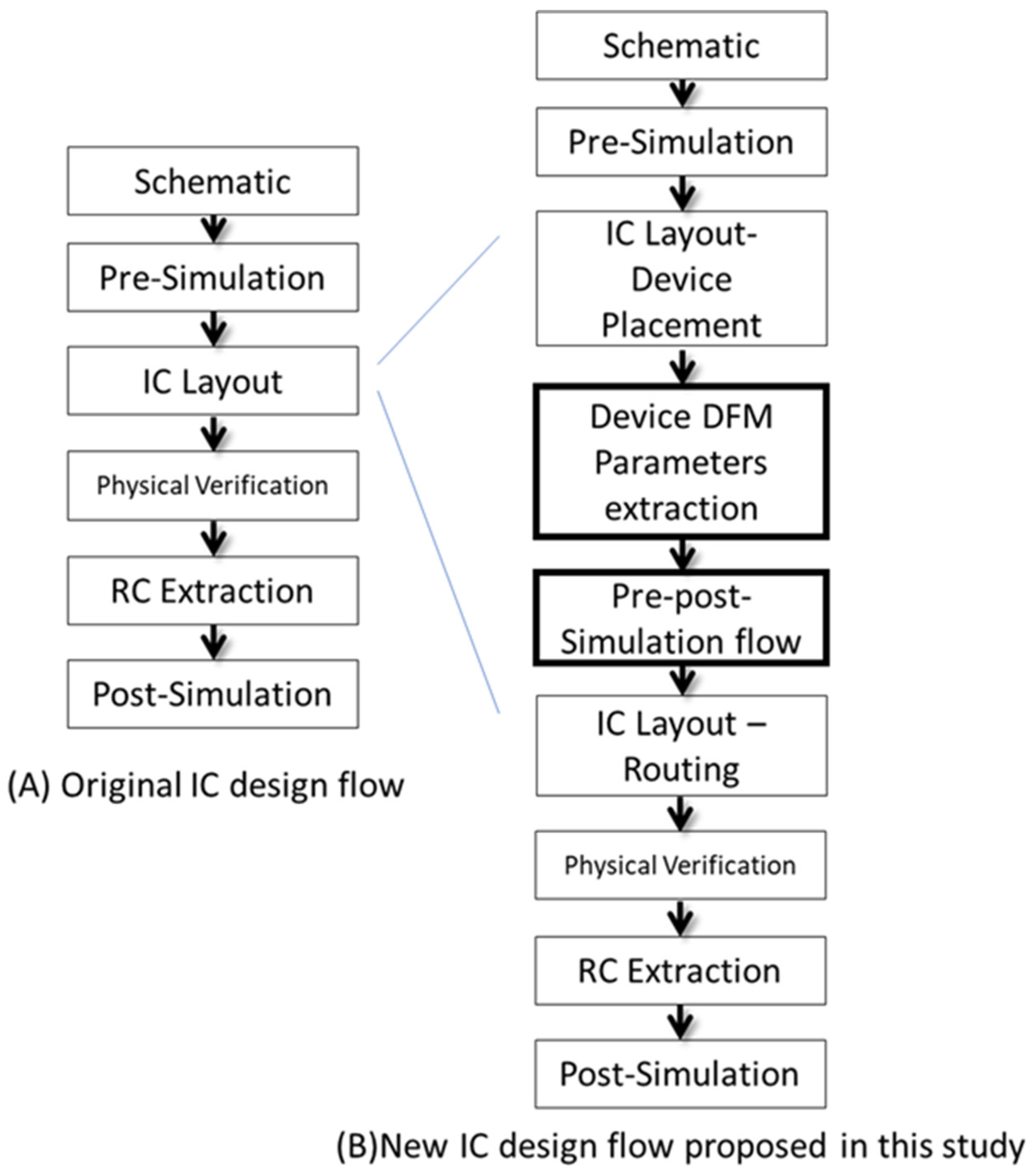
The previous section reveals that the DFM parameters of IC layouts designed in full compliance with PDK libraries may still exhibit variations due to the LDE; this is attributable to differences in IC layout environments. Therefore, this study proposed a novel IC design process for detecting and addressing DFM problems prior to routing.
Figure 5A illustrates the conventional process of Fully Custom IC design [
6,
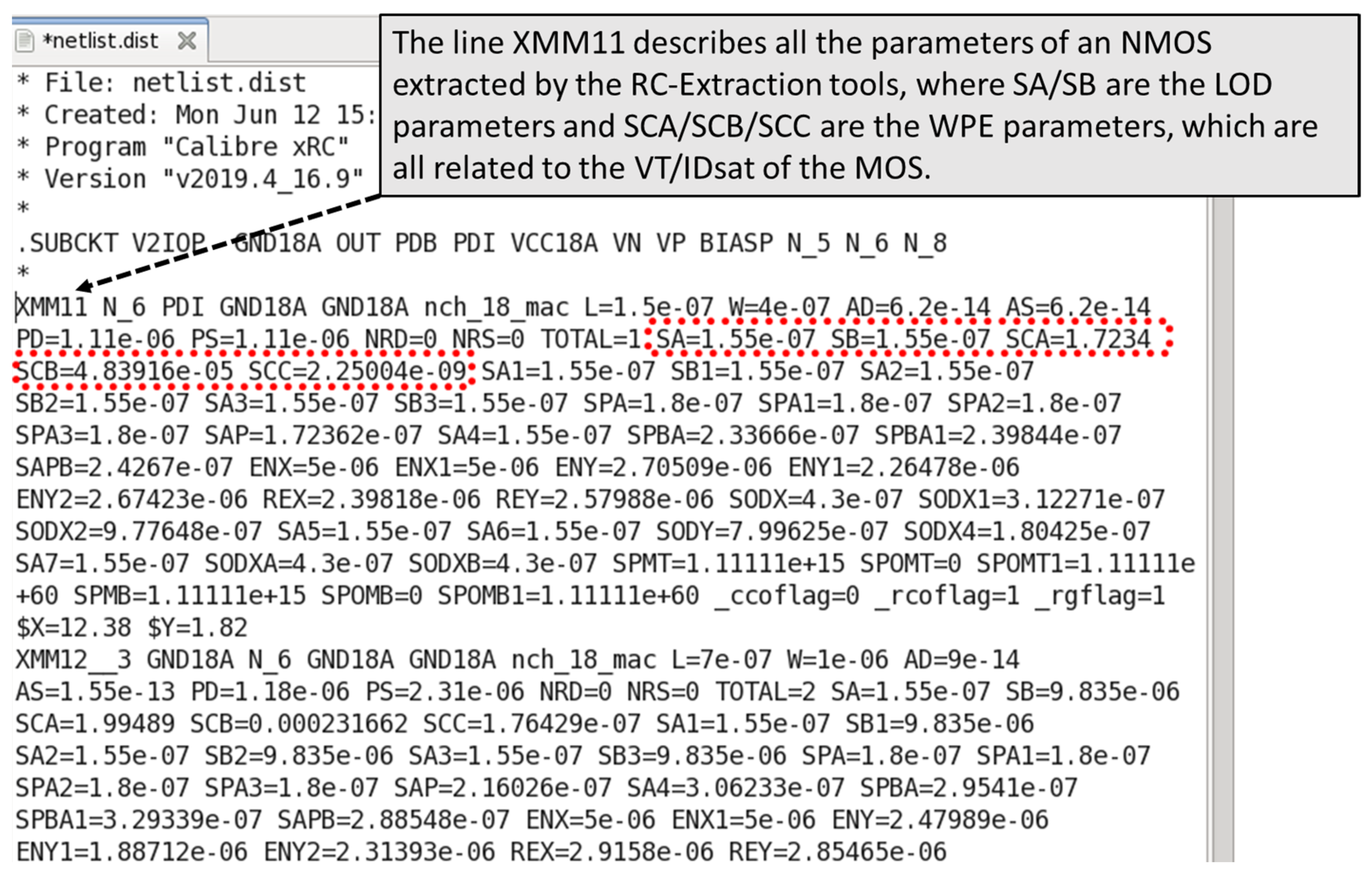
7]. After the circuit schematic is completed, simulation follows, usually referred to as the presimulation stage. Upon completion of presimulation, it proceeds to the IC layout stage, followed by physical verification, including validation processes like DRC, LVS, and ERC. Post physical verification, RC parasitic parameters are extracted. In addition to parasitic RC caused by metals, RC-Extraction tools are capable of extracting the parasitic parameters of components, including MOS channel width and length, source/drain perimeter and area. Additionally, they include DFM parameters, such as SCA, SCB, SCC affecting WPE, as well as SA, SB affecting LDE, and others.
Once these parameters are extracted using RC extraction tools, postsimulation is conducted to verify if the circuit’s functionality and efficiency meet the design specifications considering these parasitic parameters. In this process, if it is discovered only during the postsimulation phase that MOS parasitic parameters affect the circuit’s functionality, it necessitates a return to the IC Layout stage for modifications. Generally, modifying metal routing is relatively straightforward. However, when circuit functionality is affected by DFM effects, adjusting the IC Layout’s floor-plan, i.e., altering the component layout, might be necessary. Such layout modifications could even lead to the need for metal routing adjustments. Consequently, prior issues like signal line RC loading that were already adjusted need further modifications and redesigning.
After modifying the IC layout, physical verification and RC extraction need to be executed again before a subsequent postsimulation. In advanced processes, high-frequency circuits, or low-voltage designs, such iterative design cycles significantly increase time requirements.
Reference [
11] delineates the conventional DRC/LVS flow, highlighting its similarity to the traditional process depicted in
Figure 5A of this paper. Additionally, the DFM proposed in reference [
11] represents an enhancement of functionalities within DRC tools, rather than an alteration of the design workflow. This sharply contrasts with the argument we propose.
To address this issue, we propose a new design flow, as depicted in
Figure 5B, to tackle the time-consuming nature of these design iterative cycles. We pre-extract the DFM parasitic effects caused by the arrangement of devices in the IC layout before routing. Subsequently, we simulate the circuit using SPICE that incorporates the original design and DFM parameters. This combination allows us to anticipate the impact of DFM effects generated by component layout on the circuit before metal routing in the IC layout. Once ensuring these DFM issues do not affect functionality, metal routing proceeds. This approach distinctly segregates DFM issues caused by component layout from the effects of parasitic RC in metal routing on postsimulation results, effectively reducing the time required for design iterations.
As shown in
Figure 5B, a self-developed algorithm is used for the electronic design automation tool to confirm that the IC layout corresponds to the original IC design schematic. Next, the LPE phase is initiated to extract the DFM parameters of each component (excluding parasitic RC generated by routing). The resulting Simulation Program with IC Emphasis (SPICE) netlist must be confirmed to fully describe the connection relationships that ensure the integrity of the entire circuit, thereby enabling the subsequent simulation; this confirmation is called the pre-postsimulation.
The proposed process enables the detection of DFM problems in the early stages of IC design to eliminate the need for major adjustments in subsequent design stages. This approach not only facilitates the early detection of DFM problems, but also effectively isolates DFM-related issues from those associated with parasitic RC, thereby providing an efficient solution to designing and producing advanced IC devices through novel fabrication techniques.
Algorithm and Automation
IC design and layouts in advanced manufacturing processes must comply with relevant procedures in PDK libraries. In the current era in which PDKs and interoperable PDK tools are often used in IC design, various layout approaches have been proposed, such as the use of schematic-driven electronic design automation tools [
9,
12] and schematic-driven layout (SDL) flowcharts. Regarding commercially available design tools, the LakerOA and CCSE IC layout tools developed by Synopsys feature SDL functions and can be used in combination with a PDK and the interoperable PDK libraries provided by foundries. The Virtuoso tool developed by Cadence has similar functions. In this study, an algorithm was developed to achieve the proposed design process through an automation program.
In our research, we utilized the Synopsys LakerOA tool [
9]. Leveraging the SDL (Schematic-Driven Layout) concept from [
9], we connected the schematic and layout designs. SDL enables interactive communication between the schematic and layout, ensuring that all layout components generated by SDL contain information from the circuit schematic, such as NET/NOTE data. The Placement Ports functionality mentioned in the text allows for automatic port placement, aligning ports with the schematic and simplifying their arrangement. Using a program, we applied the Placement Ports feature to the ports of all components, extracting system information from various points like MOS DGSD, both endpoints of resistors, or capacitors’ endpoints. This information was annotated at each component’s endpoint, and the layout was subsequently converted into GDS. Notably, at this stage, we did not engage in metal routing.
The Standard Verification Rule Format (SVRF) manual for Siemens EDA’s Calibre [
13] on page 2339 elaborates on the Virtual Connect Colon, enabling the addition of network segment labels using text or layout text specification statements or geometric database text in the layout. Regardless of whether label names become the final network segment names, the virtual connections between labels result in virtual connections between the corresponding network segments. Specifying “yes” prompts the connection extractor to create virtual connections between any two labels with the same name. The functionality described on page 2346 [
13] as Virtual Connect Name assigns virtual connections to networks with the same name; if identical names appear in the virtual connection name statement, any set of unconnected networks will become one network. We integrated these two options into the LVS/XRC command file, activating their functionalities. This enabled Calibre LVS/XRC to treat the text on all component nodes as the same point, allowing both LVS and XRC to verify that routing was accurate. Consequently, LVS successfully and accurately performed RC extraction, achieving the desired functionality.
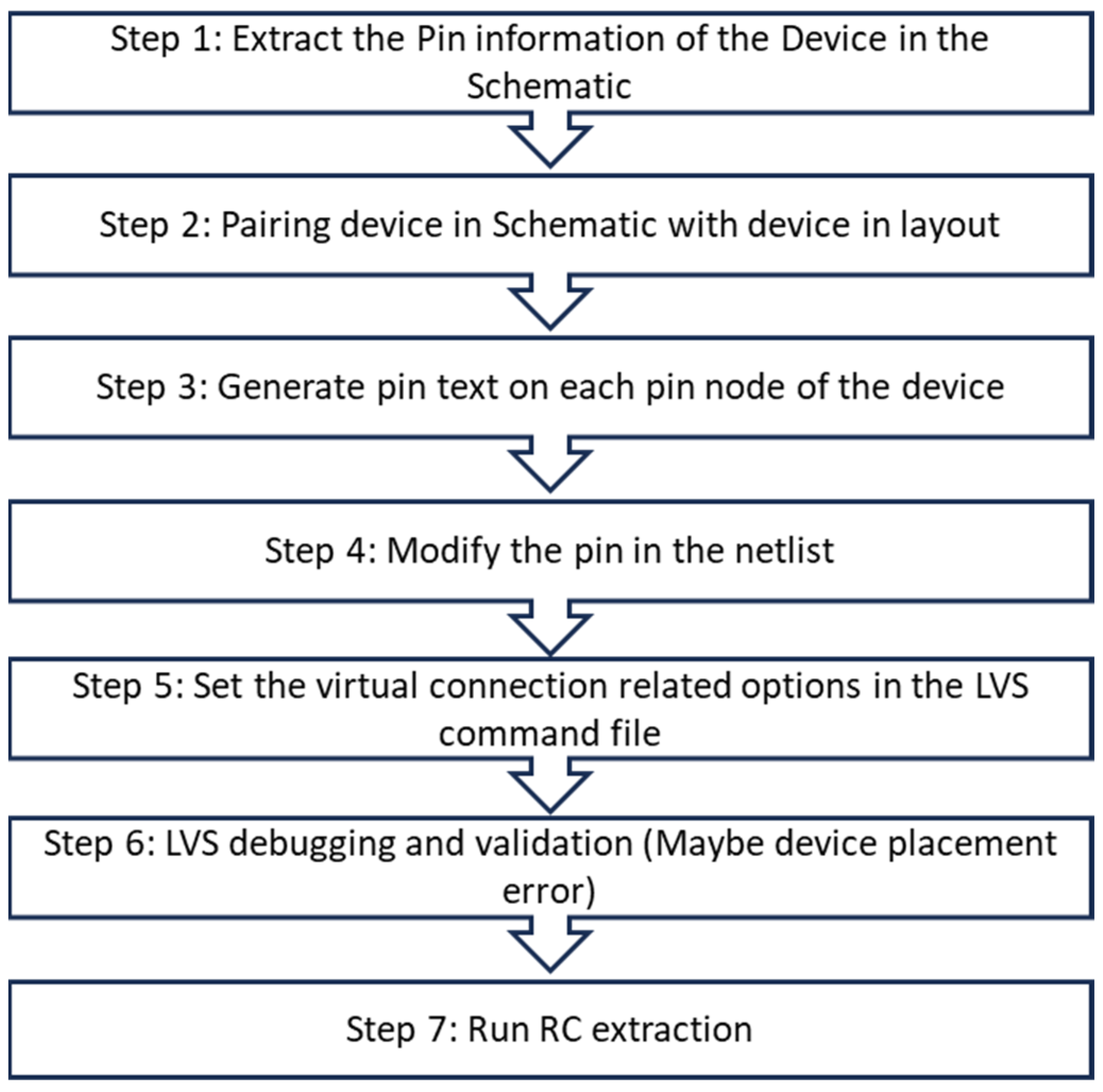
The algorithm flowchart is presented in
Figure 6: Flowchart of the proposed IC design algorithm. and is described as follows:
Step 1: All device pin information in the schematic is read.
Step 2: The SDL flow function in the IC layout tool is used in conjunction with a PDK cell. The pin information of the device enables the pairing of each device pin in the layout with that in the schematic. After all metal pins on the device have been connected, a pin layer is generated automatically.
Step 3: Pin/port text is automatically generated on each device pin to enable LVS recognition. The IC layout is output as a data graphic system file.
Step 4: The source netlist (i.e., presimulation netlist) is read, and the internal pins (i.e., nonport pins) in the schematic are added to the source netlist through the automation program.
Step 5: The automation program is used to modify the LVS command file by incorporating and enabling all LVS virtual connection-related options.
Step 6: After these five steps have been completed, the data graphic system file, netlist, and command file modified through the automation program can be used to perform LVS verification. Because all LVS virtual connection-related options have been enabled, the LVS software confirms that all pins have been connected. If the device is correctly placed in the IC layout, the LVS output must be correct.
Step 7: An RC extraction is performed to create a netlist that excludes the metal parasitic RC and includes the DFM parameters of all MOS components; this netlist is the LPE netlist required for pre-postsimulation.
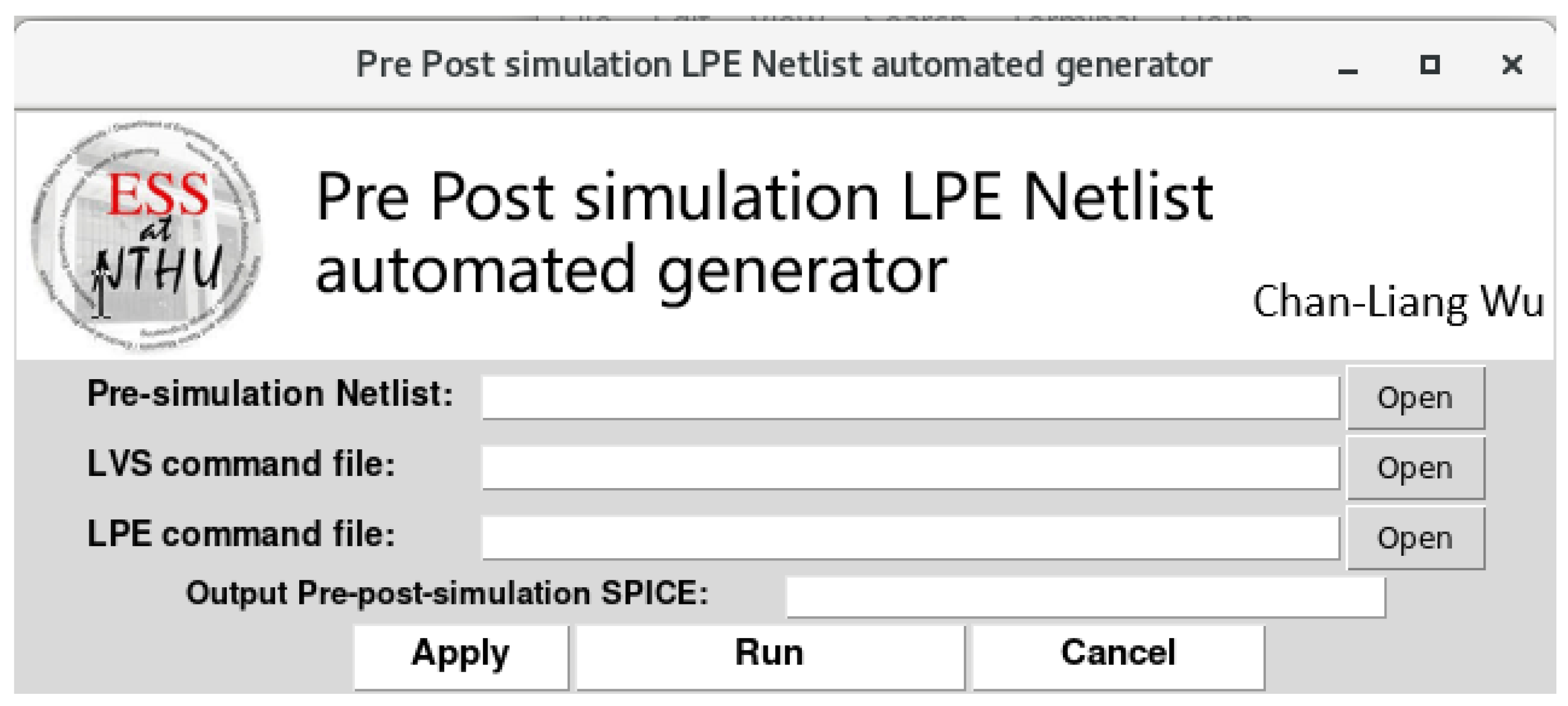
Figure 7 Interface of the automated program. After the required information is input, the program automatically processes the IC layout and generates the design file required for pre-postsimulation.
3. Results
A circuit for a current source load operational amplifier (
Figure 8) was used to test the proposed design process [
14,
15]. The design specifications were an alternating current (AC) gain of >30 db and bandwidth of >60 MHz.
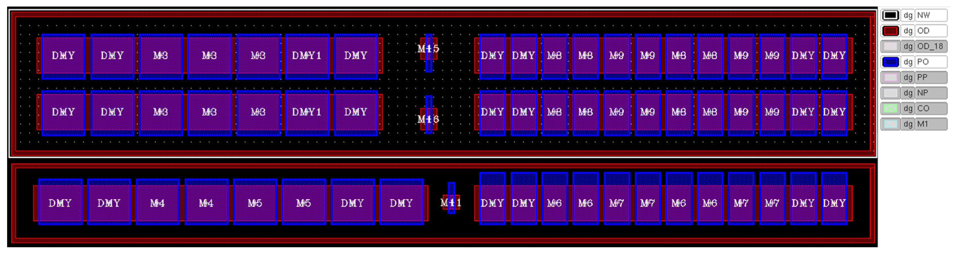
Figure 9 Development of the new IC design and layout proposed design process. In Step 1, device placement was performed for the operational amplifier circuit without conducting metal routing (
Figure 10 Device placement for the experimental IC design). The developed automation program (
Figure 7 Interface of the automated program) was next used to process the IC layout and presimulation netlist, and LPE was then performed. The DFM parameters of all components were extracted prior to metal routing (
Figure 11) to create a SPICE netlist. This netlist included all parasitic parameters, DFM parameters, and connection relationships of the components.
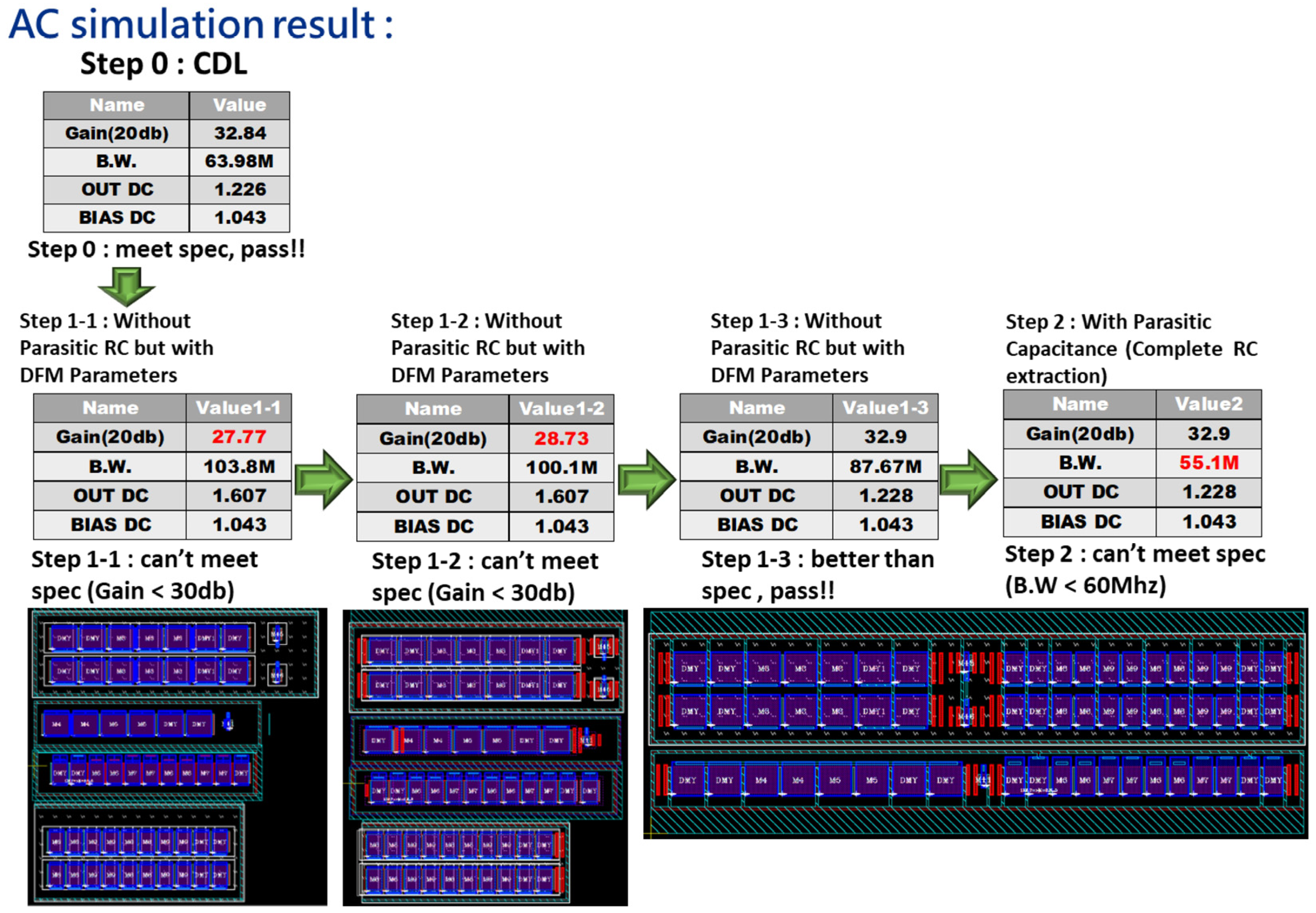
In
Figure 12 Problem convergence process for the AC simulation results of the case study, the results revealed that because of device placement and various masks (e.g., N-well, oxide diffusion, polysilicon, N-implant, and P-implant) in the three IC layout floor plans generated between Steps 1–1 and Step 1–3, the LDEs became observable in Step 1. Therefore, all parasitic effect parameters associated with device DFM were extracted before metal routing, and a simulation was performed to determine whether the current layout floor plan met the design specifications. The results obtained from Step 1–1 of the problem convergence process revealed that the floor plan did not meet the design requirements. Consequently, it was modified in Steps 1–2, which again yielded an unsatisfactory result. Therefore, the floor plan was modified again in Steps 1–3, at which point it finally met the design specifications. Metal routing was then performed in Step 2, and physical verification and LPE were conducted. Finally, a postsimulation was performed, and it revealed that the device bandwidth did not meet the design specifications. At this stage, the designer could easily confirm that the unsatisfactory bandwidth was caused by the metal routing process rather than the device placement.
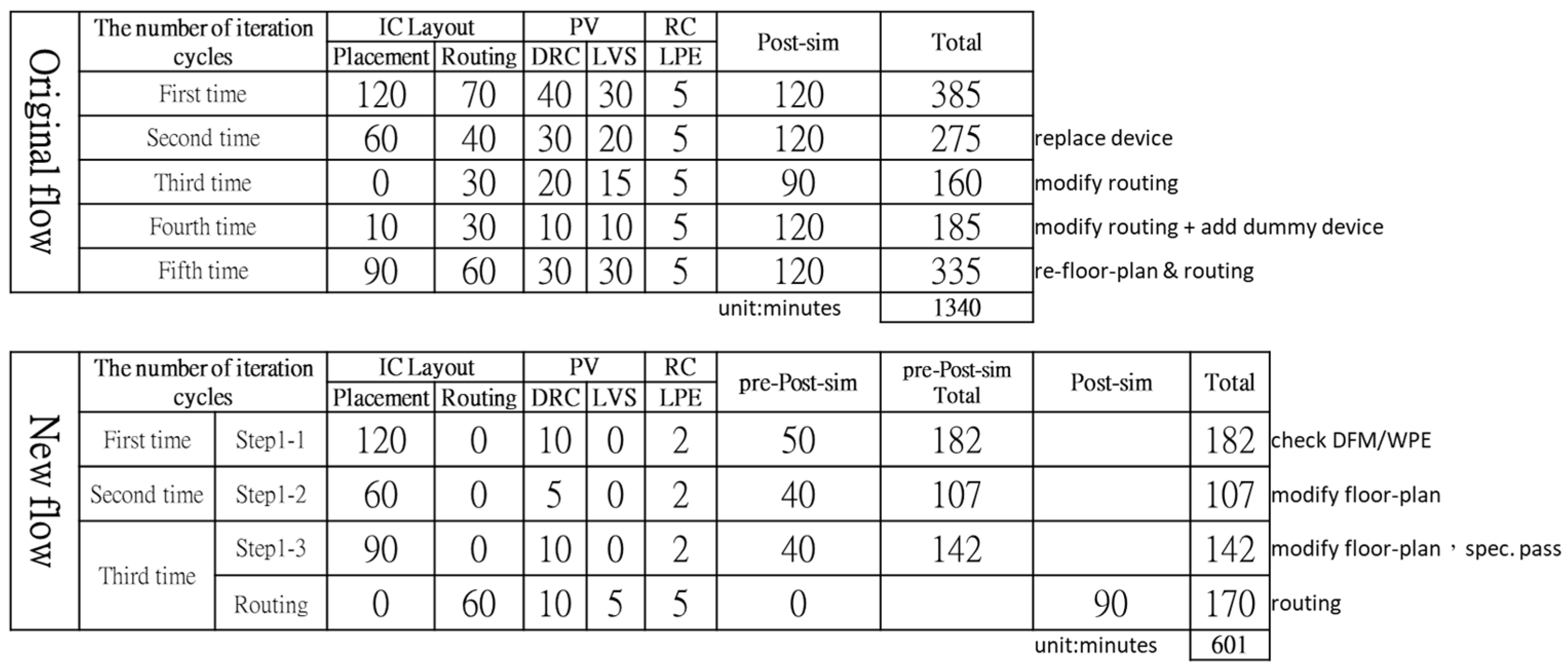
Figure 13 Experimental results indicating the benefits of the process. All of the results were collected by the same circuit designer, who assisted with the IC layout experiment. In the experiment, a conventional IC design was performed by first completing both the device placement and metal routing processes before conducting physical verification and RC extraction. In the postsimulation, the designer could not determine whether a DFM problem was caused by the device placement process or metal parasitic RC. Consequently, the device placement and metal routing processes had to be repeated, and the problems were resolved after five iteration cycles, which took 1340 min. When the proposed design process was employed, the device placement process was verified through the three-step process, and the effect of metal parasitic RC was confirmed directly after metal routing. The entire process was completed in only 601 min, less than half the time needed for the conventional design process. The proposed design process could save more time for more advanced manufacturing processes with stricter design specifications.
As shown in
Figure 13, in the conventional design process, considerable time was required to modify the floor plan after the IC layout had been determined and the metal routing process completed. This modification was extremely time-consuming because it entailed the rearrangement of nearly all metal wires.
Summary of the experimental results:
Performing Step 1 (placement, extraction, and pre-postsimulation) between Step 0 (presimulation) and Step 2 (postsimulation) is effective for revealing the effects of placement on performance.
Performance insufficiencies in Step 2 are usually attributable to routing.
This process can reduce the effort for determining an IC’s design and layout.
IC designers can directly use the pre-postsimulation SPICE netlist generated by our new design flow, which includes DFM parameters but excludes metal routing RC, to analyze the impact of DFM on circuit characteristics caused by the device layout. The proposed method provides a fast and accurate pipeline for detecting and addressing DFM problems in the early stages of the IC design process, thereby avoiding time-consuming modifications and iterations later in the process.


