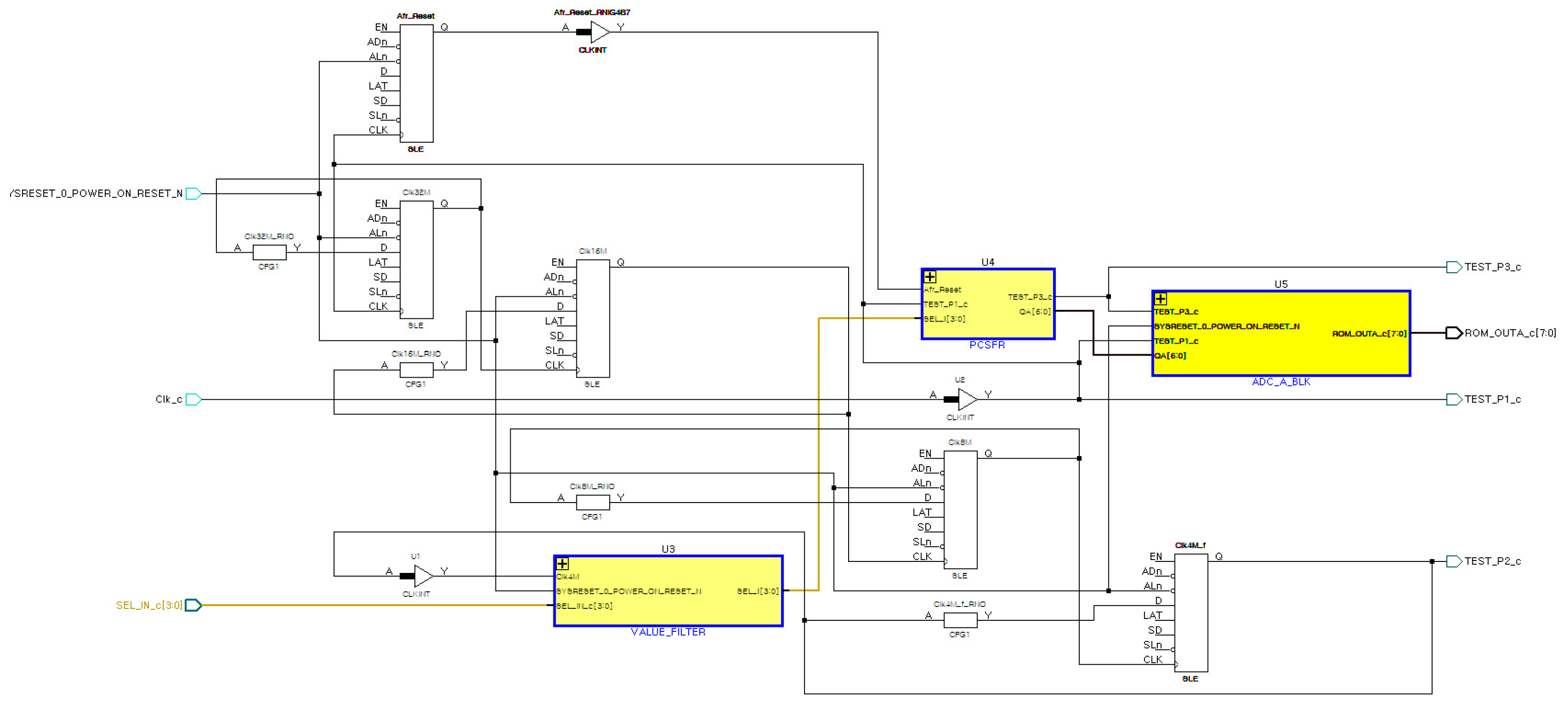
Article

A Study on the High Reliability Audio Target Frequency Generator for Electronics Industry

1
Department of Computer Engineering, Sejong University, Seoul 05006, Republic of Korea
2
Juyoung Electronic Co., Ltd., Gunpo-si 15844, Republic of Korea
3
Hyukshin Engineering Co., Ltd., Seoul 04623, Republic of Korea
4
R.O.K Cyber Operations CMD, Seoul 13834, Republic of Korea
5
Department of Convergence Engineering for Intelligent Drones, Sejong University, Seoul 05006, Republic of Korea
*
Author to whom correspondence should be addressed.
Electronics 2023, 12(24), 4918; https://doi.org/10.3390/electronics12244918
Submission received: 7 September 2023 / Revised: 20 November 2023 / Accepted: 28 November 2023 / Published: 6 December 2023
(This article belongs to the Special Issue Advances in Intelligent Data Analysis and Its Applications)

Abstract

:
The frequency synthesizer performs a simple function of generating a desired frequency by manipulating a reference frequency signal, but stable and precise frequency generation is essential for reliable operation in mechanical equipment such as communication, control, surveillance, medical, and commercial fields. Frequency synthesis, which is commonly used in various contexts, has been used in analog and digital methods or hybrid methods. Especially in the field of communication, a precise frequency synthesizer is required for each frequency band, from very low-frequency AF (audio frequency) to high-frequency microwaves. The purpose of this paper is to design and implement a highly reliable frequency synthesizer for application to a railway track circuit systems using AF frequency only with the logic circuit of an FPGA (field programmable gate array) without using a microprocessor. Therefore, the development trend of analog, digital, and hybrid frequency synthesizers is examined, and a method for precise frequency synthesizer generation on the basis of the digital method is suggested. In this paper, the generated frequency generated by applying the digital frequency synthesizer using the ultra-precision algorithm completed by many trials and errors shows the performance of generating the target frequency with an accuracy of more than 99.999% and a resolution of mHz, which is much higher than the resolution of 5 Hz in the previous study. This highly precise AF-class frequency synthesizer contributes greatly to the safe operation and operation of braking and signaling systems when used in transportation equipment such as railways and subways.

1. Introduction

Today, most devices, such as electronics, telecommunications, medical, transportation, and industrial devices, require an RF (reference frequency) inside for their original operation. This is essential for modulation and demodulation if it is a communication device, and for transmission, reception, or monitoring control processing of signals if it is a motoring control device [1]. This RF is usually generated by oscillation using the vibration of the device itself or by using the LC circuit, but the concept of a FS (frequency synthesizer) has been introduced to generate a specific frequency quickly and efficiently. There is a traditional analog method called PLL (phase-locked loop), a digital method, and a hybrid method that combines the two [2,3,4,5,6,7,8]. In this way, various technologies have been developed, from low-frequency to microwave, depending on the frequency range of frequency synthesis that produces the specific frequency desired. The output of the frequency synthesizer is very important in terms of the performance index and the accuracy of the generated frequency, which maintains stable output without shaking the generated frequency, like phase noise. For the frequency synthesizer, DDFS (direct digital frequency synthesizer), which is faster than PLL, is used to synthesize the desired frequency quickly [2]. However, the digital frequency synthesizer can synthesize the desired frequency quickly, but due to the nature of the microprocessor operated by the program mainly used here, it has a fatal flaw, such as malfunction or inoperability due to some external factors and environmental variables. For that reason, it is intentionally stuck to analog methods in industrial or highly stable special applications, not for general commercial or personal use. However, due to the various convenient characteristics of frequency synthesis, digital frequency synthesizers that can operate stably in disturbance environments such as Surge are sometimes implemented and used only by pure logic circuits without a microprocessor. Therefore, in this paper, to generate the target frequency used in the railway track circuit, the target frequency is generated using the pure logic of the FPGA to ensure the convenience, excellent performance, and safety of the digital frequency synthesizer. FPGA-based frequency synthesizers have been studied as shown in [8], but most of them deal with relatively high frequencies, and it is rare to use very low frequencies such as audio frequency bands as used in railway track circuits. In this paper, we investigate the technical development stage of frequency synthesis and its theoretical structure and design, fabricate, and simulate a frequency synthesizer with mHz deviation without a processor using only FPGA logic on the traditional structure of the digital frequency synthesizer DDFS.

2. Research and Technology Trends

DFS (direct frequency synthesis) and indirect frequency synthesis can be used to make frequency synthesizers that are essential for electronic communication devices. Direct frequency synthesis methods include direct analog synthesizers such as DAS (direct analog synthesizer) and DDFS (direct digital frequency synthesizer). Indirect frequency synthesis methods include PLL (phase-locked loop) and DLL (delay-locked loop) [6]. In addition, a hybrid FS in which two methods are mixed is used. Among the frequency generation methods, the analog method has high accuracy but difficult control, while the digital method has a simple control but low accuracy. In this section, the major frequency synthesis methods that have been studied so far, their advantages and disadvantages are examined, and the theoretical basis for implementing the improved AF frequency synthesizer is provided through the conceptual basis of DDFS using FPGA to be studied in this paper.

2.1. Analog Frequency Synthesizers

Analog frequency synthesizers can be divided into direct and indirect methods according to frequency generation methods.
The direct method is a method of generating a frequency directly from a frequency source, and the indirect method is a method of generating a necessary frequency by modulating a separately generated frequency. A direct analog frequency synthesizer is a method of generating a desired frequency by combining a reference frequency generator, a mixer, a frequency up/down converter, and a frequency doubler/multiplier, and it is a method of applying a frequency circle itself. The indirect analog frequency synthesizer generates a desired frequency using a simple technique such as inversion and frequency division and does not go through a process such as increasing another frequency source.
Andrzej Rokita [9] presented a PLL design that reduces the phase noise generated when new frequencies are generated by operations such as multiplication, mixing, filtering, and segmentation performed in direct analog synthesis. It states that very fast switching is an advantage of direct analog.
Figure 1 shows a conceptual diagram of the analog direct frequency synthesizer of [9]. In Figure 1, (a) is a method of selecting one of four oscillation frequencies as a SP4T (Single Pole 4 Transfer) switch and then multiplying it by four to obtain the desired frequency. Meanwhile, (b) is an improved method in which phase noise is reduced by (b) compared to (a) by first passing four oscillation frequencies through each of the four generators and then selecting them as switches.
In contrast, indirect frequency synthesizers are widely known and widely used PLL. PLL is a technique that compares the output signal of a VCO (voltage-controlled oscillator) with respect to an input signal and adjusts the frequency of the VCO to maintain a constant phase difference of the output signal of the VCO with respect to the input signal. In an indirect frequency synthesizer, a PLL is used to generate the desired frequency. At this time, the components of the PLL determine the performance of the frequency synthesizer.
The PLL system proposed in [1] by Yoon Kwang-sup and others includes the components of the integer-N PLL. The reference clock generated in the reference divider is compared with the VCO output signal in a PFD (phase-frequency detector) to generate an up/down signal, and a CP (charge pump) converts the up/down signal into a current and transmits it to a LF (loop filter). The LF is used to convert current to voltage and control the frequency of the VCO; the 1/N Divider in Figure 2 divides the output signal of the VCO by N to finally produce the desired frequency. Fractional-N (N) dividers are also used to combine integers and fractions to enable finer frequency control.
The advantage of this PLL system is that the spurious signal level is reduced due to the LF operation, and it is simpler than the direct analog frequency synthesizer. However, it is a disadvantage that the frequency switching time is increased and the phase noise is higher than in the direct analog method.
However, it is a disadvantage that the frequency switching time is increased and the phase noise is higher than in the direct analog method. The phase noise performance of the frequency synthesizer in the LF bandwidth can be represented by λ = λ PFD + 10logN and λ PFD is the accumulated phase noise of the reference frequency, phase detector, LF, and feedback 1/N divider inputted to the phase detector.
Yuchen Wang, Xuguang Bao, and Wei Hua have applied PLL to accurately determine the rotor position of a PMSM using a permanent magnet using the excellent phase lock capability of [10] PLL. Phase analysis of a three-phase signal is generally based on a synchronous reference system. PLL (SRF-PLL), a synchronous reference system, is the most widely used technique for extracting phase, frequency, and amplitude in a three-phase system. In this thesis, a phase shift PLL is used to map an asymmetric phase shift signal to a two-phase fixed coordinate system. In the study [11] of Kim Sang-woo and others applied to the design of a low-power frequency synthesizer for a GPS receiver using PLL, a frequency synthesizer was studied by applying a traditional fractional-N divider. Figure 3 shows the block diagram of the frequency synthesizer studied in [11]: PFD as a phase detector, CP as a charge pump, active low-pass filter, VCO, fractional-N divider, and sigma-delta modulator.
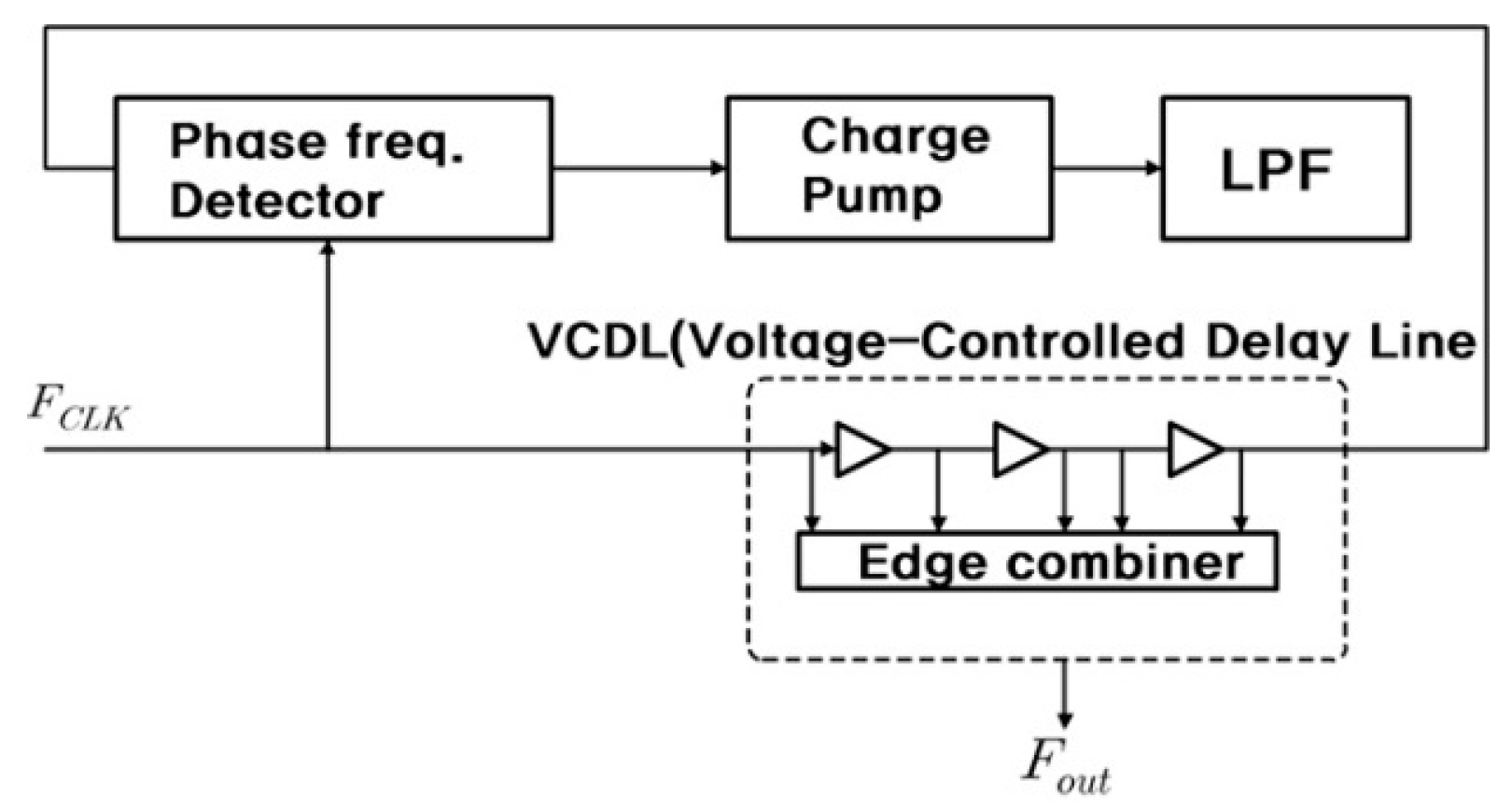
Figure 4 is a DLL-based FS block diagram, which is very similar to PLL, except that it has a VCDL (Voltage-Controlled Delay Line) instead of the VCO of PLL, and some researchers define it as a class of PLL. The idea of DLL is basically designed to solve errors related to delays that inevitably occur as the clock signal of the system goes through several stages. Despite the advantages of low noise and no phase accumulation, DLL systems are generally not recommended for FS applications due to unprogrammable, limited multiplicative factors, and high power consumption during operation [6].

2.2. Digital Frequency Synthesizers

DDFS, which takes advantage of the development of digital technology, is commonly referred to as a DDS (direct digital frequency synthesizer) and shows a simple basic configuration diagram in Figure 5 [8].
The DDS consists of a reference clock, a phase accumulator, a phase-to-amplitude LUT (look-up table), a DAC (digital-to-analog converter), a LPF (low-pass filter), and a FCW (frequency control word) that controls the output frequency.
The DDS finally produces an output signal (fout) at the reference clock frequency (fclk). This process, which mainly consists of digital control, is very fast and provides a high switching speed compared to the direct analog frequency synthesis method. DDS exhibits low-phase noise characteristics, even though the phase noise of the clock source itself is included.
In Figure 5, the frequency control word is added to the sum of the accumulator input from the phase accumulator and calculated, and the value is implemented in the bit adder and the result is supplied to the accumulator register.
On the one hand, the waveform data, in which the value sent as the sample address corresponds to the phase-amplitude conversion circuit, is outputted according to the address value. It is transformed through the D/A converter and LPF to the analog waveform and waveform data is outputted
The biggest advantage of this DDS is that the output frequency of the Heltz (Hz) level is generated by the fine frequency resolution due to the phase accumulator, but the limitation of available bandwidth and spurious performance are disadvantages. At this time, the highest possible frequency is limited to less than half of the clock frequency by the Nyquist theorem, and spurious noise is higher than the analog frequency synthesis method due to quantization and DAC conversion errors.
A.A. Alsharef et al. implemented the typical DDS of Figure 6 in FPGA (field programmable gate array) in [12]. FPGA is a device that is composed of unit blocks called CLB (Configurable Logic Block) rather than individual logic devices. It can be used as a desired input and output by the user, thereby reducing the complexity of hardware circuits and increasing reliability. The DDS using FPGA is designed as a LUT consisting of a Verilog code, which is also composed of PA, LUT, and D/A and simulated by the RTL (register transfer language) model.
Matt Bergeron and Alan N. Willson, Jr. studied 1 GHz DDS on FPGA in [13]. The fast orthogonal DDS implemented with the FPGA is based on a new multiplier-based angle rotation algorithm that does not distort the magnitude of the sine and cosine outputs. The algorithm is designed to be well mapped to the DSP slices present in the FPGA. The device is implemented in the Xilinx Virtex-7 device and consumes 54.9 mW at 1 GHz, a performance previously only achieved in the ASIC design.
Another study using FPGA proposed a frequency synthesizer with a frequency resolution of 1.5 kHz, with a power consumption of 3.96 mW and a spurious performance of 59 dBc in the quadrature DDS of [14] studied by M. Saber Saber, M. Elmasry, and M. Eldin Abo-Elsoud.
In this study, ROM is not used for low-power implementation during operation on the FPGA. A simple approach that compensates for the shortcomings of the converter from phase to amplitude in the structure of a typical DDS, as shown in Figure 6, is to use a ROM with a function called LUT; however, as shown in the following formula:
f o u t = W 2 L F c l k
  • L: bit number of accumulator
  • W: bit value of input frequency word
In general, to achieve fine frequency tuning, several techniques have been devised to limit the ROM size while maintaining adequate performance to require large values, one of which is to reduce the number of angles required for the sine amplitude to four using a quarter-wave symmetry of the sine function. Cutting out the output of the phase accumulator leads to spurious noise, but this approach is commonly used because it achieves a fine frequency resolution that requires a very large value for L.
To reduce the memory size in LUT-based FS, various angular decomposition methods have been proposed, which typically consist of dividing the ROM into several small units, each of which is processed as part of the truncated phase accumulator output. Data searched in each low-rank ROM is added, and the sine curve approximation value is produced. Therefore, the proposed structure in [14] states that the sine function is divided into linear segments, each segment has a linear equation, and the value of this equation is obtained through additional hardware.
Wenjun Chen et al. [15] studied how to implement DDS performance improvement with the CORDIC (coordinated rotation digital computer) algorithm. They used XILINX’s FPGA to reduce the output delay by repeatedly merging into a small amount of ROM, which can be seen to realize a sinusoidal wave with an SFDR of 86.76 dB at a high frequency of 350 MHz. Yixiong Yang et al. propose the LUT-ROT (rotation) architecture of traditional DDS in [16]. In order to optimize the speed and area of 2 GHz DDS, a performance of 11.7 mW/GHz is implemented in an area of 0.016 mm2 by pipelined LUT.

2.3. Hybrid Frequency Synthesizers

A mixture of analog and digital frequency synthesizer structures has been studied in both direct and indirect methods, first using DDS in the direct analog frequency synthesis mentioned above, as shown in Figure 6.
In the analog method, DDS can be added to the input unit to reduce the complexity of the design and the overall components, and then DDS can be inserted instead of the fractional-N divider in the PLL system. It is a kind of mixed system of PLL and DDS. In the study [3] analyzing the phase noise of the digital hybrid PLL frequency synthesizer, the input noise to obtain the minimum phase noise, the D/A conversion noise due to the quantization error, and the mathematical model of the VCO noise source were derived and analyzed.
In order to improve the performance of the high-resolution beam-forming receiver based on DDS and PLL, Ref. [4] implements high-phase resolution by applying 14 bits of DDS.
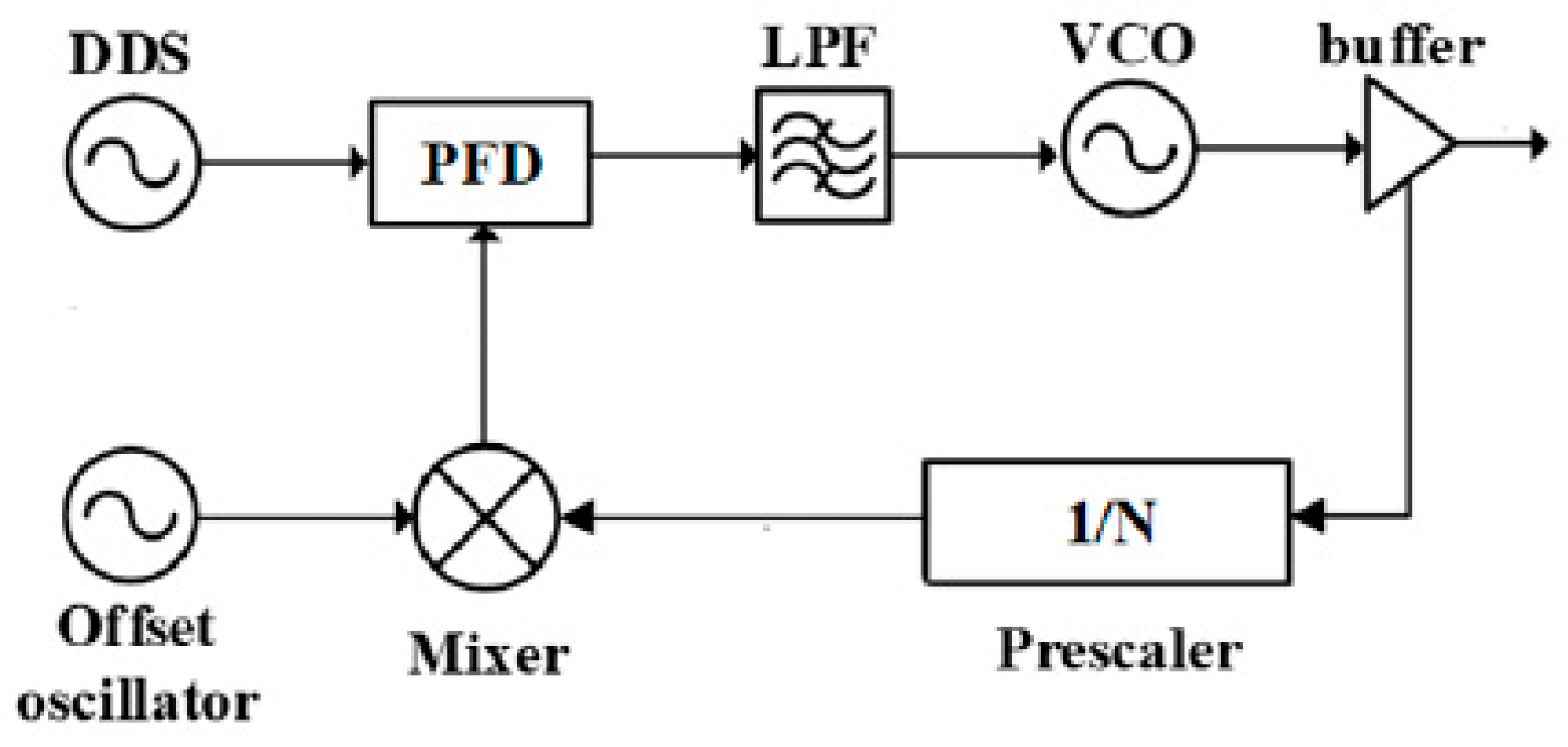
In [4], the implementation of beamforming using only the existing DDS was implemented using DDS-PLL, as shown in Figure 7.
In the high-performance PLL FS (Frequency Synthesizer) [17] applied to the radar system studied by Kim Song-sik and others, the D/A of the DDS was applied for the PLL modeling design to realize excellent phase noise and high-speed frequency synthesis time in the broadband characteristics. In order to compensate for the disadvantages of general PLL FS, we provide a coarse tune through D/A of DDS. Akila Gothandaraman and Syed K. [18] proposed an all-digital frequency locked loop (ADFLL) that eliminates analog shortcomings by implementing all PLL digitally.
In this study, an algorithm to frequency synthesize ADFLL capable of high-speed frequency acquisition is proposed to reduce hardware cost and architecture, enable full digitization, and become a pulse-output DDFS that is easy to design and implement. In addition, an adaptive phase estimator is proposed to show that the DDFS has a 16-bit binary weighting control, and the simulation results show that the ADFL can operate in the frequency range between 50 MHz and 500 MHz.

3. Design of DDFS for Low Frequency Using FPGA

3.1. Necessity

As we have seen so far in related studies, various methods of frequency synthesizers are used for their advantages and disadvantages. As discussed in Section 2, the application range of FPGA-based DDS to be studied in this paper is gradually increasing due to reliability and convenience of development. Railways and subways use AF (audio frequency) track circuit devices that accurately detect the track driving of a train and perform train control and monitoring in a specific section.
Currently, the AF track circuit device used in railways is a modulation-demodulation transmission system that modulates and transmits a specific audible frequency of 30 Hz or less. It has been 20 to 30 years since it was used as an analog method using LC oscillation. It is time to change to a more precise digital method. In this paper, we study the frequency synthesizer for the design and fabrication of audio frequency generation equipment that generates the desired audible frequency in order to produce a frequency synthesizer that generates the audible frequency accurately and stably. In this paper, we propose and implement DDS using an FPGA and a pure logic circuit without a microprocessor in order to implement a stable device free from external noise. The accuracy of frequency synthesis is confirmed by simulation.
As shown in Figure 8, the reference clock A and the frequency control word (FCW) input to the PA (phase accumulator) are determined by the input of the frequency control word. The output of the PA is converted into a sinusoidal amplitude value in a look-up table (LUT) stored in the ROM, and a pure sinusoidal frequency is generated using a digital–analog converter (DAC) and an LPF. The frequency at this time is defined by the following equation [13].
F o u t = F C W 2 L F C L K
  • FCW: Frequency control word
  • L: The number of bits of PA
In this case, the resolution of the frequency tends to increase as the reference clock frequency is small and the number of PA bits is large, as shown in the following equation. The frequency resolution of DDS can be defined as the reference clock frequency divided by the bit of the accumulator, which can be expressed by the following equation:
Δ F = F C L K 2 L
Therefore, it is necessary to properly limit the size of the ROM with a large L value for fine tuning and precise frequency generation.

3.2. Target Frequency

In the proposed system in Figure 9, the stability of the reference clock is very important, so a high-frequency X-tal must be used to generate the reference clock. This crystal oscillator, which is supplied for industrial use, is very stable due to its low temperature coefficient in the range of −40–120 °C. The reference frequency composed of the crystal oscillator generates the frequency of 1 kHz∼6 kHz required for the track circuit and changes it to a TWS (thumb-wheel switch) attached to the side of the simulation device. The oscillation frequency is generated within 0.05% of the target accuracy, and the desired frequency can be obtained by changing the TWS value.
The frequency generated in this way can be applied to various fields, but in this study, the frequency used for the railway AF track circuit is generated. The AF track circuit frequency modulates and transmits FSK (frequency shift keying), and the reception demodulates it to detect and analyze the transmitted frequency to determine whether there is a train in the corresponding track circuit section. That is, when the frequency is detected, it is judged that there is no train in the corresponding track circuit section, and if the detection is not performed, it is judged that there is a train. FSK is a frequency shift modulation method in which data selects different frequencies between 0 and 1 according to a frequency having a constant amplitude.
If the frequency shift is A, the following equation becomes the FSK modulated signal.
S(t) = Acos2π(fC − Δf)t:0 ≤ tT:1
S(t) = Acos2π(fC − Δf)t:0 ≤ tT:0
where A is the amplitude of the FSK, fC is the center frequency of the carrier frequency, and Δf is the deviation frequency.
The receiver recognizes two sinusoidal frequencies, which are carriers, in advance, extracts the corresponding frequencies, and restores the modulation frequency, which is called demodulation. This method is less defective than ASK (amplitude shift keying), and the circuit is relatively simple, so it is widely used in transmission equipment such as the AF track circuit device used in railways. In the track circuit device of the railway, the modulation frequency is fixed at 4.8 Hz, and the carrier frequency has eight center frequencies in consideration of the subway line and the upper and lower lines and modulates two frequencies of 17 Hz for the upper shift frequency and 17 Hz for the lower shift frequency of the center frequency. The track circuit frequency combination of the railway is shown in Figure 9.
These track circuit frequencies are used in Europe and Asia, and the Bombardier specification [19] specifies the transmission and receiver frequency arrangement, as shown in Table 1 below.
(1)
Algorithm design
In this paper, we find and implement the optimal frequency generation algorithm after several trials and errors. This algorithm first generates the target frequency of Hz unit resolution by passing through D-FF 13 times, which has the function of delaying the desired generation frequency 8192 times by the time interval of the clock pulse. Specific methods and configurations, such as circuits and FPGA blocks, for simulating this method are described below. The circuit required for the algorithm generating the AF track circuit frequency is shown in Figure 10.
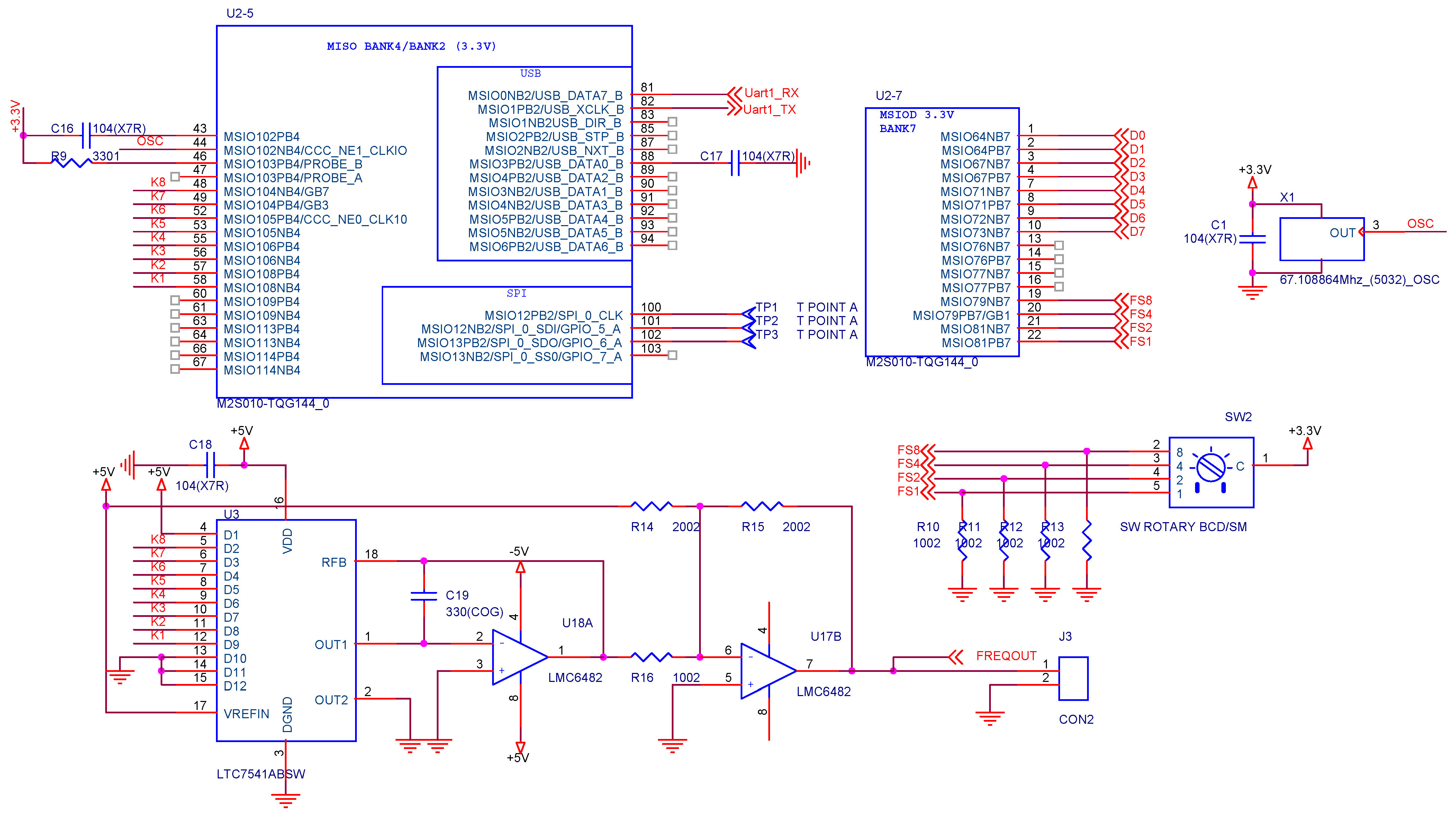
The M2S010 of the upper left part consists of an FPGA, and the right equivalent part uses an X-tal of 67.108864 Mhz as a reference clock generator. The lower left part represents a digital analog converter and an LPF. In the middle of the right side is a TWS that selects the frequency as the rotary switch.
The 8-bit FPGA output is converted to an analog signal using AD7541 from analog devices, a D/A converter.
The FPGA output is converted to 8 bits by a D/A converter called AD7541 from an analog device company.
According to the selection of the TWS, one frequency corresponding to the orbital frequency (upper and lower sides of A–H) according to the Bombardier standard is generated, and the upper frequency and the lower frequency can be composed of two frequency outputs generating the same method.
A logic block called ADC_A_OUT with a built-in look-up table (LUT) value is implemented as an FPGA, and a digital output of 256 steps is generated by this logic block. This result is applied to the AD7541 input, which is a digital-to-analog conversion IC, and is output as an analog signal.
In order to obtain the analog sine wave output signal, the D-FF (Flip Flop) is performed 13 times in the logic block called DCOUNT13 in the FRGEN block inside the FPGA to have a duty ratio of 50:50. This output is the SW2 of Figure 11, and 16 frequencies can be selected from 0 to F, and the frequency output according to the switch position is designed as shown in Table 1.
(2)
FPGA logic blocks
A. Configuring I/O ports
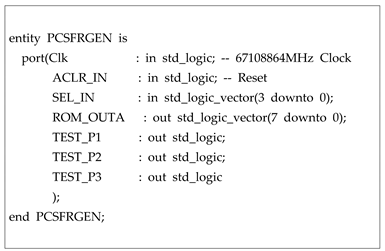
The input/output port has an oscillator clock, a reset, and a frequency selection switch input as input units, and an output unit has an 8-bit digital frequency and three test terminals.
Electronics 12 04918 i001
B. Component configuration
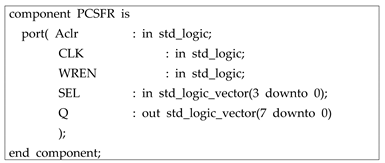
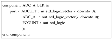
The components of the internal logic consist of PCSFR, Value_filter, ADC_A and clock buffer, and the components except for the clock buffer are configured as follows:
Electronics 12 04918 i002
Electronics 12 04918 i003
Electronics 12 04918 i004
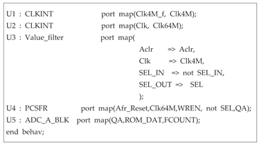
The connection process of the component is as follows:
Electronics 12 04918 i005
C. Configuration logic compilation
Compiled blocks of the entire FPGA internal use are captured and shown in the figure below.
Figure 11. Block diagram of compilation.
Electronics 12 04918 g011
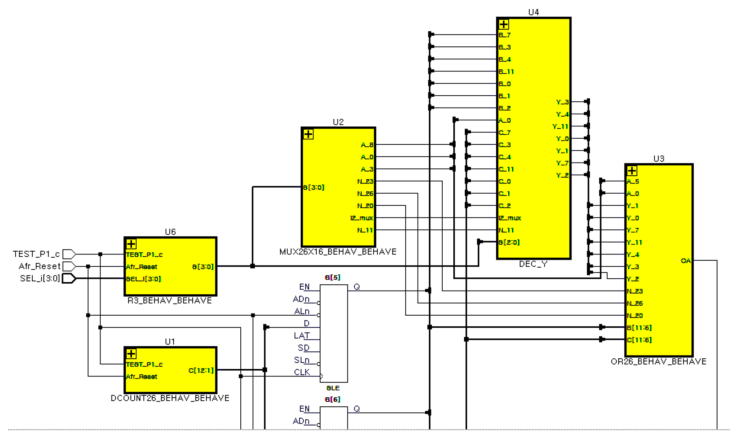
In the entire compile block of Figure 11, terminals for input and output are connected to the PCSFRGEN block. The inside of the PCSFRGEN block is configured as shown in Figure 12 below.
Figure 13 is composed of the value filter logic block created for chattering, protecting the switch input of the input unit, and the frequency generator, Figure 14 and Figure 15 show the FRGEN logic block and the ADC A OUT logic block having an 8-bit look-up table for the sine wave output. Each of the configured compile blocks is shown below.
Figure 15 is a detailed compiled block of this block, and the details are divided into Figure 16 and Figure 17.
Figure 15. ADC_A_OUT (look-up table) compilation block diagram.
Electronics 12 04918 g015
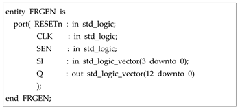
The FRGEN block may be referred to as a set of initial logic for frequency generation (Figure 14). The logic configuration and the compiled capture circuit of each part thereof are as follows:
Electronics 12 04918 i006
The split block diagram of Figure 16 is shown in Figure 17 and Figure 18.
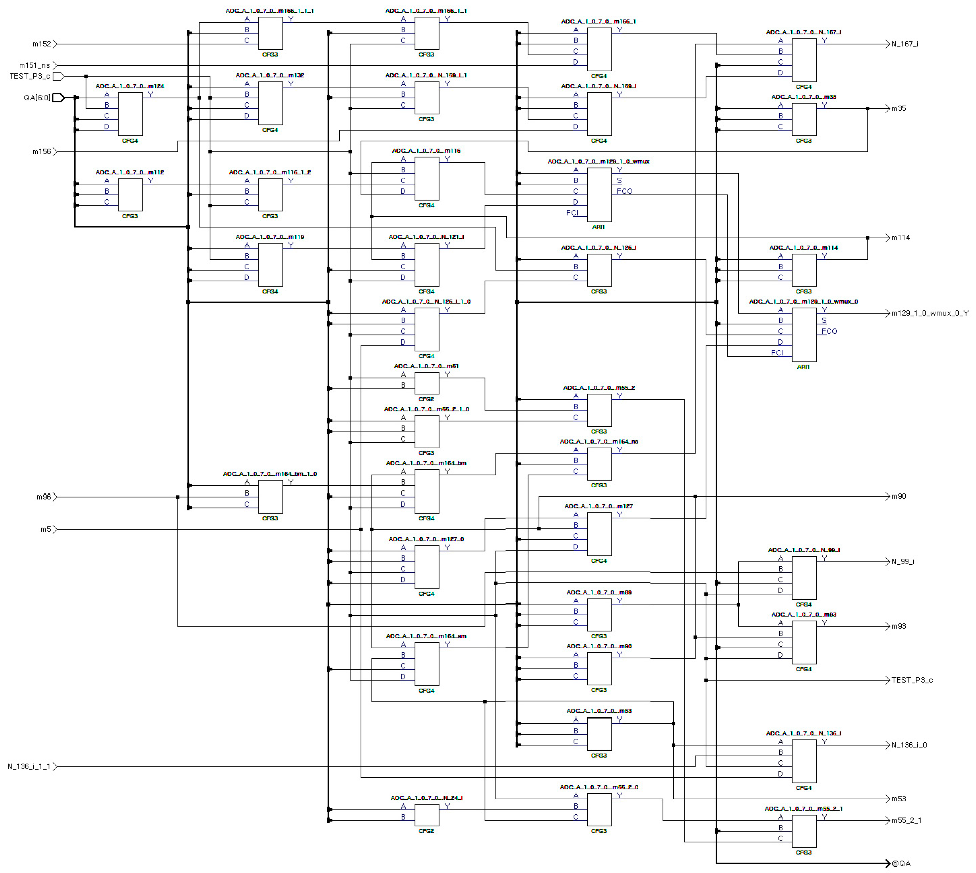
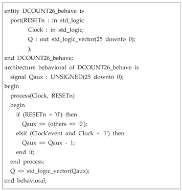
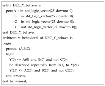
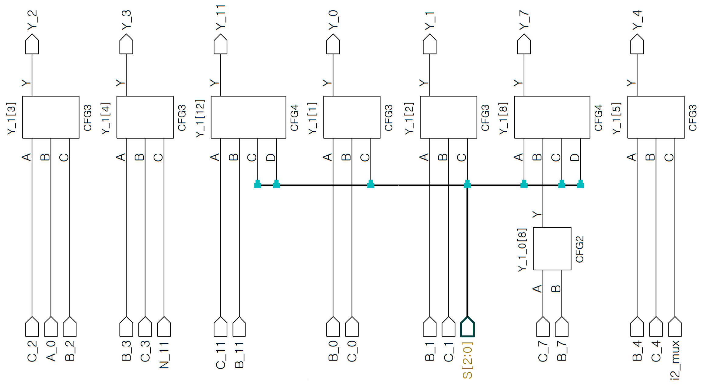
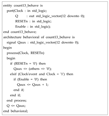
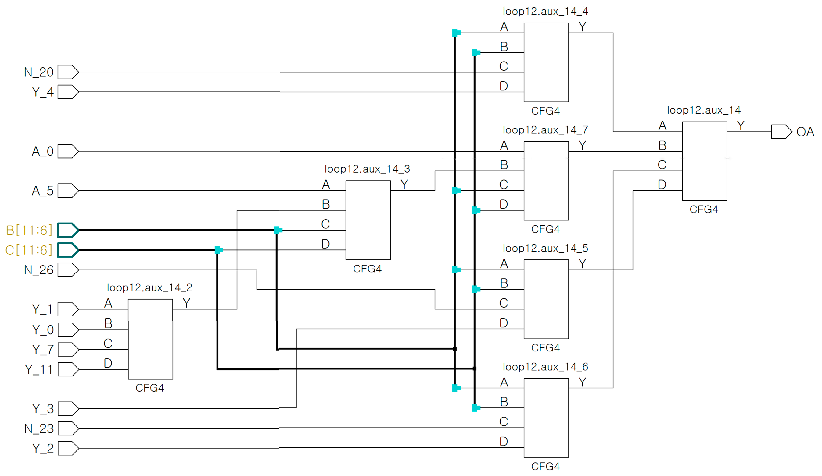
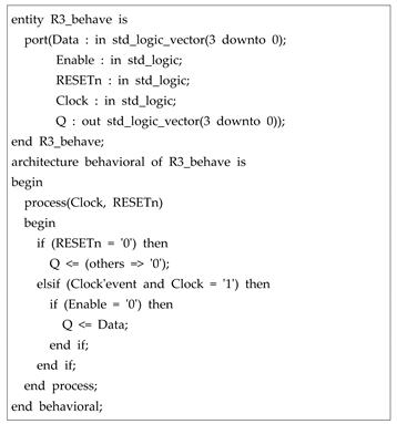
The detailed composition of Figure 16 FRGEN consists DCOUNT26 in Figure 19, DEC_Y in Figure 20, MuX26x8 in Figure 21, COUNT13 in Figure 22, OR2 in Figure 23 and R3 in Figure 24, logic blocks and each picture and compilation source is shown below.
Figure 16. FRGEN compilation detail block diagram.
Electronics 12 04918 g016
Figure 17. FRGEN compilation partial block Diagram 1.
Electronics 12 04918 g017
Figure 18. FRGEN compilation partial block Diagram 2.
Electronics 12 04918 g018
The composition of the internal components is as follows:
Electronics 12 04918 i007
Figure 19. DCOUNT26 compilation block.
Electronics 12 04918 g019
Electronics 12 04918 i008
Figure 20. DEC_Y compilation block diagram.
Electronics 12 04918 g020
Figure 21. MUX26x8 compilation block diagram.
Electronics 12 04918 g021
Electronics 12 04918 i009
Electronics 12 04918 i010
Figure 22. COUNT13 compilation block diagram.
Electronics 12 04918 g022
(3)
Track circuit use frequency generation
The 13 bits used to generate the target frequency are generated more accurately toward the MSB (Most Significant Bit) of the up counter treated with the FPGA of Figure 23, so the upper 8 bits are used and the duty ratio is designed to be 50:50 using the LSB (Least Significant Bit) 5 bits. Thus, the generated frequency follows the following equation:
LC Frequency(FLCF) = k/25
  • LC: Track circuit as a line circuit
  • k: Bits extracted with the target frequency
Electronics 12 04918 i011
Figure 23. OR26 compilation block diagram.
Electronics 12 04918 g023
Electronics 12 04918 i012
Figure 24. R3 compiles internal block diagram.
Electronics 12 04918 g024
The output upper 8 bits are input to a DAC circuit (AD7541) and converted into an analog sine wave output, and the converted signal is generated as an audio frequency output to output a complete sinusoidal frequency.
The FPGA chip of the proposed system uses the Smart -Fusion2 SoC M2S010 [19] of Microchip Co., Ltd. The maximum usable logic device of this chip is composed of 12,084 highly integrated system chip ICs.
The M2S010 is designed for low power consumption and is a chip device that provides excellent reliability and security for multipurpose applications such as video image processing, I/O expansion and conversion, and Gigabit Ethernet. The ARM series MPU is also built-in, but this proposed system is not used because of its high reliability. Figure 25. Shows the internal block diagram of the M2S010.
It shows a product composed of circuits designed in Figure 26.
Refer to the description of the main part in the right clockwise direction of the used substrate, FPGA chip, test terminal, JTAG interface terminal, and X-tal oscillator. From the upper left, the description is the power input terminal, the frequency change SW, the reset SW, the output terminal, and the analog waveform output IC. The 10-pin JTAG Interface Terminal on the lower right is used to input the program to the FPGA.
In implementing the frequency accuracy, we show that the circuit used in this simulation works very well, as shown in the results of the following Section 4. The circuit configuration is very simple, but the result shows that the method of verifying the envisioned algorithm is suitable. Therefore, it can be seen from the related picture that the desired precise frequency is output by this configuration. The results of the experiment were measured and recorded by selecting the frequency with the octal frequency change switch, and the output frequency was described in detail in the experimental results.

4. Experimental Results

After repeated trials and errors in the method of optimally generating the target frequency processed by the FPGA logic block, the results of the following equations were verified.
Y = 1 C L O C K × 2 13 × 2 26 × F r e q u e n c y
By implementing the practical structure and algorithm that precisely creates the AF band DDFS used in railway track circuits with FPGA, we show that 16 frequencies currently used in Europe and Korea are implemented with a precision of 99.9980%~99.9996%, and this is shown as a simulation result.
As a result of the simulation, it was confirmed that a stable and accurate frequency output with a frequency deviation superior to the target error range was made. Compared to the results of previous studies using FPGAs with a deviation of 5 Hz in the range of [8] 0–160 kHz, it shows that it is much better than the deviation of 1~2 Hz, which is [20] of the Bombardia product specification. The results can be seen in Table 2 and Table 3.

Simulation

As shown in Figure 27, the board was connected and operated.
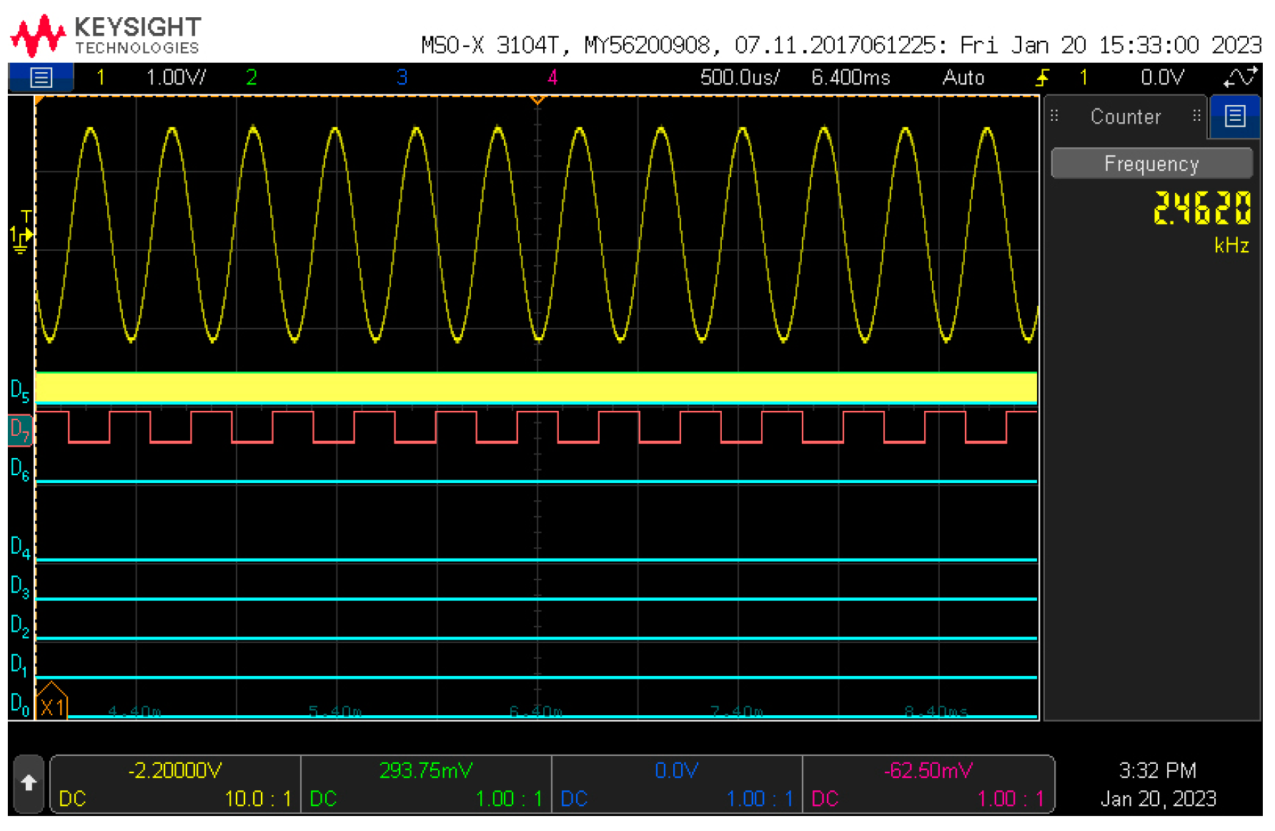
The output results observed while turning the TWS for frequency change on the right side of the test board are shown in Figure 28 and Figure 29:
(1)
Track frequency A test results and waveforms
Figure 27. Simulation.
Electronics 12 04918 g027
Figure 28. Lower frequency 1682 Hz generated waveform.
Electronics 12 04918 g028
Figure 29. Upper frequency 1716 Hz generated waveform.
Electronics 12 04918 g029
The signal waveform of the ADC7541 A/D converter output is 100 − (100 × (1682.0007 − 1682)/1682) = 99.9999%, and the upper frequency accuracy is shown in Table 2.
The simulation results and waveforms from the track circuit generation frequency B to H can be confirmed in the attached Appendix A.

5. Conclusions

In this paper, we propose a method to implement AF for railway track circuits in DDS using a microchip FPGA. This frequency generator is composed of pure logic circuits without using a general CPU, minimizing the factors of malfunction and suggesting the possibility of increasing safety in key industries. By proposing a practical structure and algorithm that precisely creates DDFS in the AF band, 16 frequencies currently used in railway track circuits are implemented with a precision of 99.9980–99.9996%, and these are shown as simulation results. This proves that the performance is superior to the 5 Hz deviation of the previous study [8].
It was able to generate very stable and accurate frequency output, and it is judged that it will be possible to make a precise frequency generator with high reliability in the field of key industries such as railways. These results are expected to enhance the safety and user convenience of the control system in key industries such as railways. In the future, it is expected that the research on multiple AF DDFS that generate multiple frequencies at the same time by developing this study will be practically useful in various industries.

Author Contributions

Conceptualization, C.P. and E.H.; methodology, E.H.; software, E.H.; validation, C.P. and E.H.; formal analysis, C.P.; investigation, C.P.; resources, C.P.; data curation, C.P.; writing—original draft preparation, C.P.; writing—review and editing, I.K.; visualization, D.S.; supervision, D.S.; project administration, D.S. All authors have read and agreed to the published version of the manuscript.

Funding

This work was supported by the National Research Foundation of Korea (NRF) grant funded by the Korea government (MSIT) (No. 2022R1F1A1074773).

Data Availability Statement

Data are contained within the article.

Conflicts of Interest

The authors declare no conflict of interest. The companies had no role in the design of the study; in the collection, analyses, or interpretation of data; in the writing of the manuscript; or in the decision to publish the results.

Appendix A

In this section, measurement results from Group B to Group H among the simulation results in Table 2 are described.
(1)
Track frequency B test results and waveforms
Figure A1. Lower frequency 2279 Hz generated waveform.
Electronics 12 04918 g0a1
Figure A2. Upper frequency 2313 Hz generated waveform.
Electronics 12 04918 g0a2
The signal waveform shown in the ADC7541 A/D conversion circuit output is 100 − (100 × (2279.0043 − 2279)/2279) = 99.9998% compared with the lower frequency value designed with the frequency of 2279 Hz when the TWS (thumb-wheel switch) is located at 1, and the upper frequency accuracy is shown in Table 2.
(2)
Track frequency C test results and waveforms
Figure A3. Lower frequency 1979 Hz generated waveform.
Electronics 12 04918 g0a3
Figure A4. Upper frequency 2013 Hz generated waveform.
Electronics 12 04918 g0a4
The signal waveform shown in the ADC7541 A/D conversion circuit output is 100 − {100 × (1979.0036 − 1979)/1979} = 99.9998% compared with the lower frequency value designed with the frequency of 2279 Hz when the TWS (thumb-wheel switch) is located at 1, and the upper frequency accuracy is shown in Table 2.
(3)
Track frequency D test results and waveforms
Figure A5. Lower frequency 2576 Hz generated waveform.
Electronics 12 04918 g0a5
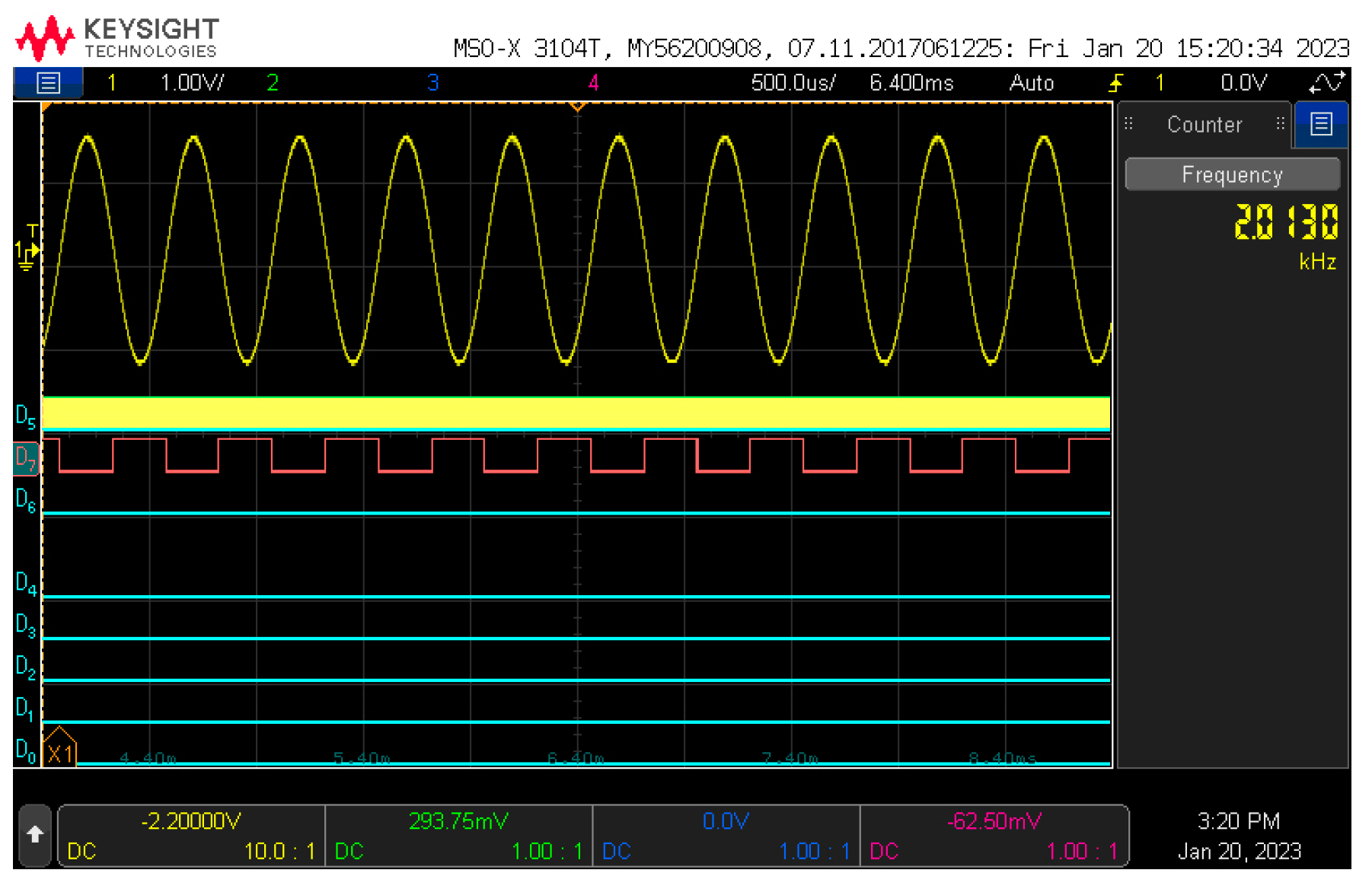
Figure A6. Upper frequency 2610 Hz generated waveform.
Electronics 12 04918 g0a6
The signal waveform shown in the ADC7541 A/D conversion circuit output is 100 − {100 × (2576.0030 − 2576)/2576} = 99.9998% compared with the lower frequency value designed with the frequency of 2279 Hz when the TWS (thumb-wheel switch) is located at 1, and the upper frequency accuracy is shown in Table 2.
(4)
Track frequency E test results and waveforms
Figure A7. Lower frequency 1532 Hz generated waveform.
Electronics 12 04918 g0a7
Figure A8. Upper frequency 1566 Hz generated waveform.
Electronics 12 04918 g0a8
The signal waveform shown in the ADC7541 A/D conversion circuit output is 100 − {100 × (1532.0026 − 1532)/1532} = 99.9998% compared with the lower frequency value designed with the frequency of 2279 Hz when the TWS (thumb-wheel switch) is located at 1, and the upper frequency accuracy is shown in Table 2.
(5)
Track frequency F test results and waveform
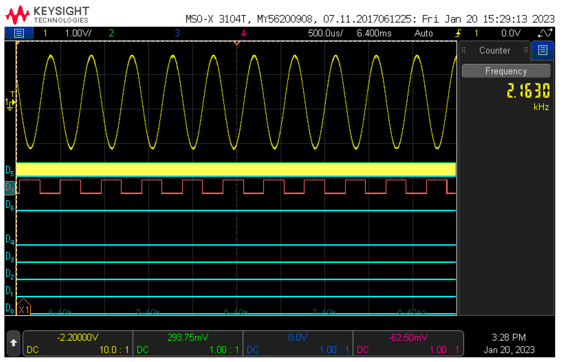
Figure A9. Lower frequency 2129 Hz generated waveform.
Electronics 12 04918 g0a9
Figure A10. Upper frequency 2163 Hz generated waveform.
Electronics 12 04918 g0a10
The signal waveform shown in the ADC7541 A/D conversion circuit output is 100 − {100 × (2129.0021 − 2129)/2129} = 99.9999% compared with the lower frequency value designed with the frequency of 2279 Hz when the TWS (thumb-wheel switch) is located at 1, and the upper frequency accuracy is shown in Table 2.
(6)
Track frequency G test results and waveforms
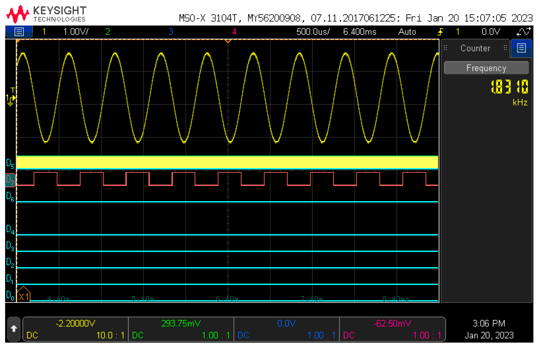
Figure A11. Lower frequency 1831 Hz generated waveform.
Electronics 12 04918 g0a11
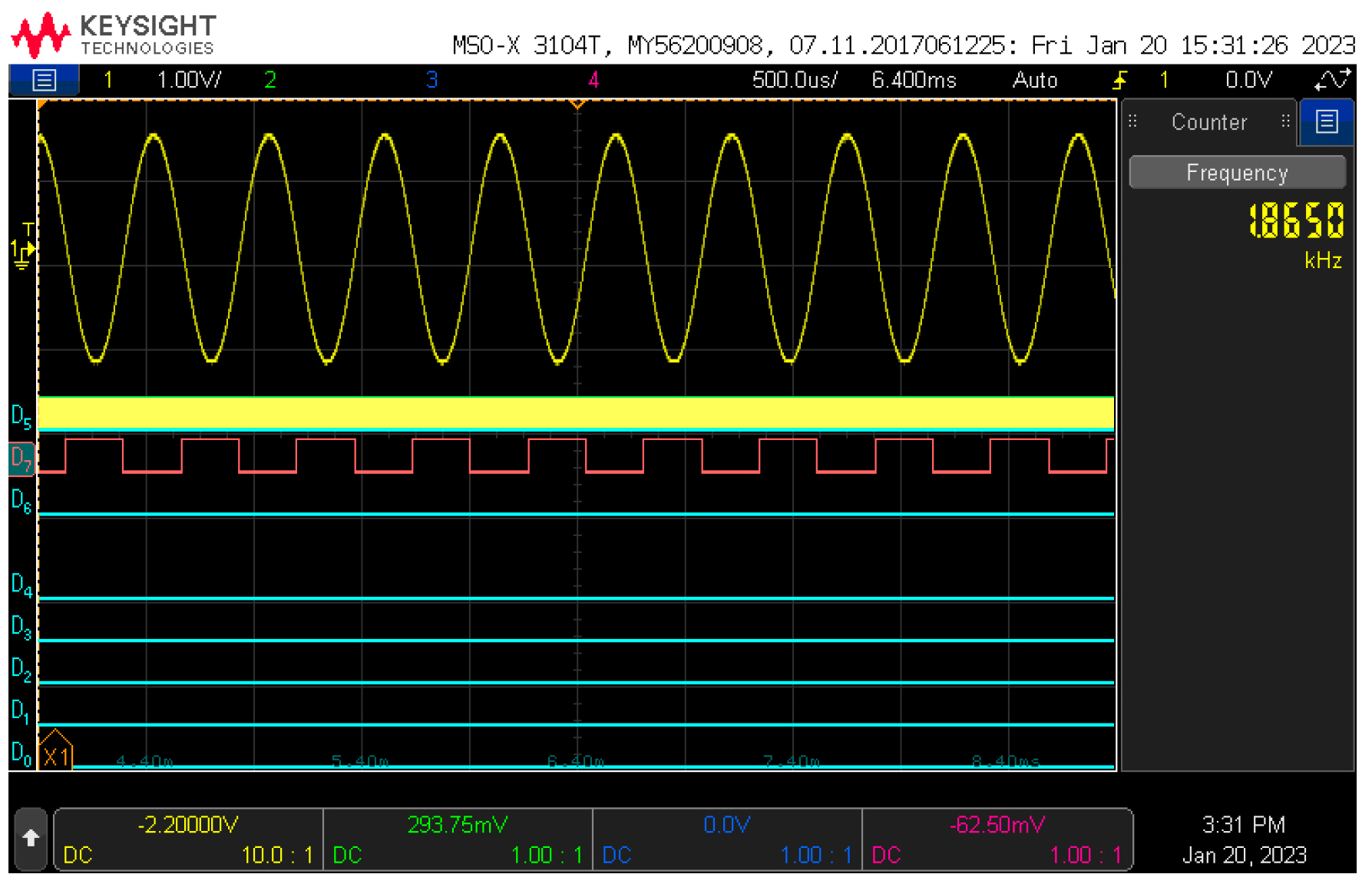
Figure A12. Upper frequency 1865 Hz generated waveform.
Electronics 12 04918 g0a12
The signal waveform shown in the ADC7541 A/D conversion circuit output is 100 − {100 × (1831.0037 − 1831)/1831} = 99.9998% compared with the lower frequency value designed with the frequency of 2279 Hz when the TWS (thumb-wheel switch) is located at 1, and the upper frequency accuracy is shown in Table 2.
(7)
Track frequency H test results and waveforms
Figure A13. Lower frequency 2428 Hz generated waveform.
Electronics 12 04918 g0a13
Figure A14. Upper frequency 2462 Hz generated waveform.
Electronics 12 04918 g0a14
The signal waveform shown in the ADC7541 A/D conversion circuit output is 100 − {100 × (2428.0057 − 2428)/2428} = 99.9997% compared with the lower frequency value designed with the frequency of 2279 Hz when the TWS (thumb-wheel switch) is located at 1, and the upper frequency accuracy is shown in Table 2.

References

  1. Yoon, K.; Song, M.; Noh, J.; Lee, K. Design of Data Converters and PLL; Hongneung Science Publishing House: Daejeon, Republic of Korea, 2013; pp. 299–324. [Google Scholar] [CrossRef]
  2. Tierney, J.; Radre, C.M.; Gold, B. A Digital Frequency Synthesizer. IEEE Trans. Audio Electro Acoust. 1971, AU-19, 49–50. Available online: https://ieeexplore.ieee.org/abstract/document/1162151 (accessed on 27 November 2023).
  3. Ryu, H.G.; Lee, H.S. Analysis and Minimization of Phase Noise of The Digital Hybrid PLL Frequency Synthesizer. IEEE Trans. Consum. Electron. 2002, 48, 305–306. Available online: https://ieeexplore.ieee.org/abstract/document/1010136 (accessed on 27 November 2023).
  4. Kim, D.C.; Chi, Y.E.; Park, J. High-Resolution Digital Beamforming Receiver Using DDS–PLL Signal Generator for 5G Mobile Communication. IEEE Trans. Antennas Propag. 2022, 70, 1429–1430. Available online: https://ieeexplore.ieee.org/abstract/document/9539071 (accessed on 27 November 2023). [CrossRef]
  5. Queiroz, E.D.; Ota, J.I.Y.; Pomilio, J.A. State-Space Representation Model of Phase-Lock Loop Systems for Stability Analysis of Grid-connected Converters. In Proceedings of the 14th IEEE International Conference on Industry Applications 2021, São Paulo, Brazil, 15–18 August 2021; pp. 388–389. Available online: https://ieeexplore.ieee.org/abstract/document/9529609 (accessed on 27 November 2023).
  6. Akurwy, S.H. A Novel ROM Design for High Speed Direct Digital Frequency Synthesizer; Lap Lambert Academic Publishing: Saarbrücken, Germany, 2014; pp. 6–15. [Google Scholar]
  7. Gao, S.; Barnes, M. Phase-locked loops for grid-tied inverters: Comparison and testing. In Proceedings of the 8th IET International Conference on Power Electronics, Machines and Drives (PEMD 2016), Glasgow, UK, 19–21 April 2016; Available online: https://digital-library.theiet.org/content/conferences/10.1049/cp.2016.0304 (accessed on 27 November 2023).
  8. Shan, C.; Chen, Z.; Yuab, H.; Hu, W. Design and Implementation of a FPGA-based Direct Digital Synthesizer. In Proceedings of the 2011 International Conference on Electrical and Control Engineering, Yichang, China, 16–18 September 2011; pp. 614–615. Available online: https://ieeexplore.ieee.org/abstract/document/6057152 (accessed on 27 November 2023).
  9. Rokita, A. Direct Analog Synthesis Modules for an X-Band Frequency Source; Telecommunications Research Institute: Daejeon, Republic of Korea, 1997; pp. 63–64. Available online: https://ieeexplore.ieee.org/abstract/document/737920 (accessed on 27 November 2023).
  10. Wang, Y.; Bao, X.; Hua, W. Implementation of Embedded Magnetic Encoder for Rotor Position Detection Based on Arbitrary Phase Shift Phase Lock Loop. IEEE Trans. Ind. Electron. 2002, 69, 2035–2037. Available online: https://ieeexplore.ieee.org/abstract/document/9369043 (accessed on 27 November 2023). [CrossRef]
  11. Kim, S.; Kim, J.; Oh, H.; Cheon, J.; Park, G.; Go, S.; Lee, K. Design of Low Power Frequency Synthesizer for GPS Receiver. Korea Inst. Intell. Transp. Syst. 2008, 11a, 165–168. [Google Scholar]
  12. Alssharef, A.A.; Ali, M.A.M.; Sanusi, H. Direct Digital Frequency Synthesizer Design and Implementation on FPGA. Res. J. Appl. Sci. 2012, 7, 387–390. [Google Scholar] [CrossRef]
  13. Bergeron, M.; Willson, A.N. A 1-GHz Direct Digital Frequency Synthesizer in an FPGA. In Proceedings of the 2014 IEEE International Symposium on Circuits and Systems (ISCAS), Melbourne, VIC, Australia, 1–5 June 2014; pp. 329–332. Available online: https://ieeexplore.ieee.org/abstract/document/6865132 (accessed on 27 November 2023).
  14. Saber, M.S.; Elmasry, M.; Abo-Elsoud, M.E. Quadrature Direct Digital Frequency Synthesizer Using FPGA. In Proceedings of the 2006 International Conference on Computer Engineering and Systems, Cairo, Egypt, 5–7 November 2006; pp. 14–15. Available online: https://ieeexplore.ieee.org/abstract/document/4115478 (accessed on 27 November 2023).
  15. Chen, W.; Wu, T.; Tang, W.; Jin, K.; Huang, G. Implementation Method of CORDIC Algorithm to Improve DDFS Performance. In Proceedings of the IEEE 3rd International Conference on Electronics Technology 2020, Chengdu, China, 8–12 May 2020; pp. 58–61. Available online: https://ieeexplore.ieee.org/abstract/document/9119621 (accessed on 27 November 2023).
  16. Yang, Y.; Wang, Z.; Yang, P.; Chang, M.F.; Ho, M.S.; Yang, H.; Liu, Y. A 2-GHz Direct Digital Frequency Synthesizer Based on LUT and Rotation. In Proceedings of the 2018 IEEE International Symposium on Circuits and Systems (ISCAS), Florence, Italy, 27–30 May 2018; pp. 1–3. Available online: https://ieeexplore.ieee.org/abstract/document/8351207 (accessed on 27 November 2023).
  17. Kim, D.; Lee, H.; Kim, J.; Kim, S. Design and Modeling of a DDS Driven Offset PLL with DAC. Korea Internet Broadcast. Commun. Soc. 2012, 12, 1–9. [Google Scholar] [CrossRef]
  18. Gothandaraman, A.; Islam, K.S. An All-Digital Frequency Locked Loop (ADFLL) with a Pulse Output Direct Digital Frequency Synthesizer (DDFS) and an Adaptive Phase Estimator. In Proceedings of the IEEE Radio Frequency Integrated Circuits Symposium 2003, Philadelphia, PA, USA, 9–10 June 2023; pp. 303–305. Available online: https://ieeexplore.ieee.org/abstract/document/1213949 (accessed on 27 November 2023).
  19. Bombardier. EBI Track 200 TI21 Audio Frequency Track Circuit Technical Manual; Bombardier: Montreal, QC, Canada, 2019; Available online: https://docplayer.net/28867426-Ebi-track-200-ti21-audio-frequency-track-circuit.html (accessed on 27 November 2023).
  20. Microchip. FPGA and SoC Product Families; Microchip Technology Inc.: Chandler, AZ, USA, 2019; pp. 3–5. Available online: http://ww1.microchip.com/downloads/en/DeviceDoc/00002871B.pdf (accessed on 27 November 2023).
  21. Transport RailCorp. TI21 Track Circuit Test and Investigation Guideline; Transport RailCorp: Sydney, NSW, Australia, 2016; pp. 13–14. Available online: https://www.transport.nsw.gov.au/industry/asset-standards-authority/find-a-standard/ti21-track-circuit-test-and-investigation (accessed on 27 November 2023).
Figure 1. Block diagram of analog direct frequency synthesizer.
Electronics 12 04918 g001
Figure 2. Basic structure of PLL frequency synthesizer.
Electronics 12 04918 g002
Figure 3. Application structure of PLL frequency synthesizer.
Electronics 12 04918 g003
Figure 4. Frequency synthesizer block diagram based on DLL.
Electronics 12 04918 g004
Figure 5. Direct digital frequency synthesizer basic diagram.
Electronics 12 04918 g005
Figure 6. Conceptual diagram of DAFS with DDS added.
Electronics 12 04918 g006
Figure 7. DDS-PLL block diagram.
Electronics 12 04918 g007
Figure 8. Basic structure of the proposed system.
Electronics 12 04918 g008
Figure 9. Track circuit frequency composition used in railways.
Electronics 12 04918 g009
Figure 10. Circuit diagram required to implement the algorithm.
Electronics 12 04918 g010
Figure 12. PCSFRGEN compilation block diagram.
Electronics 12 04918 g012
Figure 13. Value_filter compilation block diagram.
Electronics 12 04918 g013
Figure 14. FRGEN compilation block diagram.
Electronics 12 04918 g014
Figure 25. Internal block diagram of M2S010.
Electronics 12 04918 g025
Figure 26. Circuit board used for testing.
Electronics 12 04918 g026
Table 1. Bombardier track circuit frequency array.
Frequency NameCenter
Frequency (Hz)
Frequency
Separation
Frequency (Hz) ±5%Note
A1699Lower Freq.(FL)16821699 − 17
Upper Freq.(FH)17161699 + 17
B2296Lower Freq.(FL)22792296 − 17
Upper Freq.(FH)23132296 + 17
C1996Lower Freq.(FL)19791996 − 17
Upper Freq.(FH)20131996 + 17
D2593Lower Freq.(FL)25762593 − 17
Upper Freq.(FH)26102593 + 17
E1549Lower Freq.(FL)15321549 − 17
Upper Freq.(FH)15661549 + 17
F2146Lower Freq.(FL)21292146 − 17
Upper Freq.(FH)21632146 + 17
G1848Lower Freq.(FL)18311848 − 17
Upper Freq.(FH)18651848 + 17
H2445Lower Freq.(FL)24282445 − 17
Upper Freq.(FH)24622445 + 17
Table 2. Simulation result.
ItemTarget Design
Frequency (Hz) (±0.05%)
Test Result
Frequency (Hz)
Accuracy (%)Note
016821682.000799.99995838A
117161716.000999.99994755
222792279.004399.99981132B
323132313.006999.99970169
419791979.003699.99981809C
520132013.000999.99995529
625762576.003099.99986025D
726102610.005299.99980077
815321532.002699.99983029E
915661566.004799.99969987
A21292129.002199.99990136F
B21632163.003799.99982894
C18311831.003799.99979792G
D18651865.003899.99979625
E23282428.005799.99976904H
F24622462.005699.99977254
Table 3. Simulation result comparison.
Comparison With Existing Research and ProductsFrequency
Deviation
AccuracyNote
A Study on the High Reliability Audio Target Frequency
Generator
0.001~0.006 Hz0.001%This Research Paper
Design and Implementation of a FPGA-based Direct Digital
Synthesizer
+5 Hz~−5 Hz0.30%Reference [11]
Bombardier TI21 Track Circuit Test and Investigation
Guideline
1 Hz~2 Hz0.06~0.12%Reference [21]
Disclaimer/Publisher’s Note: The statements, opinions and data contained in all publications are solely those of the individual author(s) and contributor(s) and not of MDPI and/or the editor(s). MDPI and/or the editor(s) disclaim responsibility for any injury to people or property resulting from any ideas, methods, instructions or products referred to in the content.