
Segment Reduction-Based Space Vector Pulse Width Modulation for a Three-Phase F-Type Multilevel Inverter with Reduced Harmonics and Switching States


Abstract
:1. Introduction
- (a)
- Nine- and three-segment SVPWM algorithms different from conventional CBPWM are developed for an FT2LI.
- (b)
- The array of switching state transitions and profiles is broadly studied in detail for various SVPWM algorithms and compared with CBPWM.
- (c)
- An analysis and comparison of the magnitude of harmonic concentration around the switching frequency in CBPWM and segment reduction-based SVPWM in FT2LI are discussed.
2. Implementation of SVPWM for FT2LI
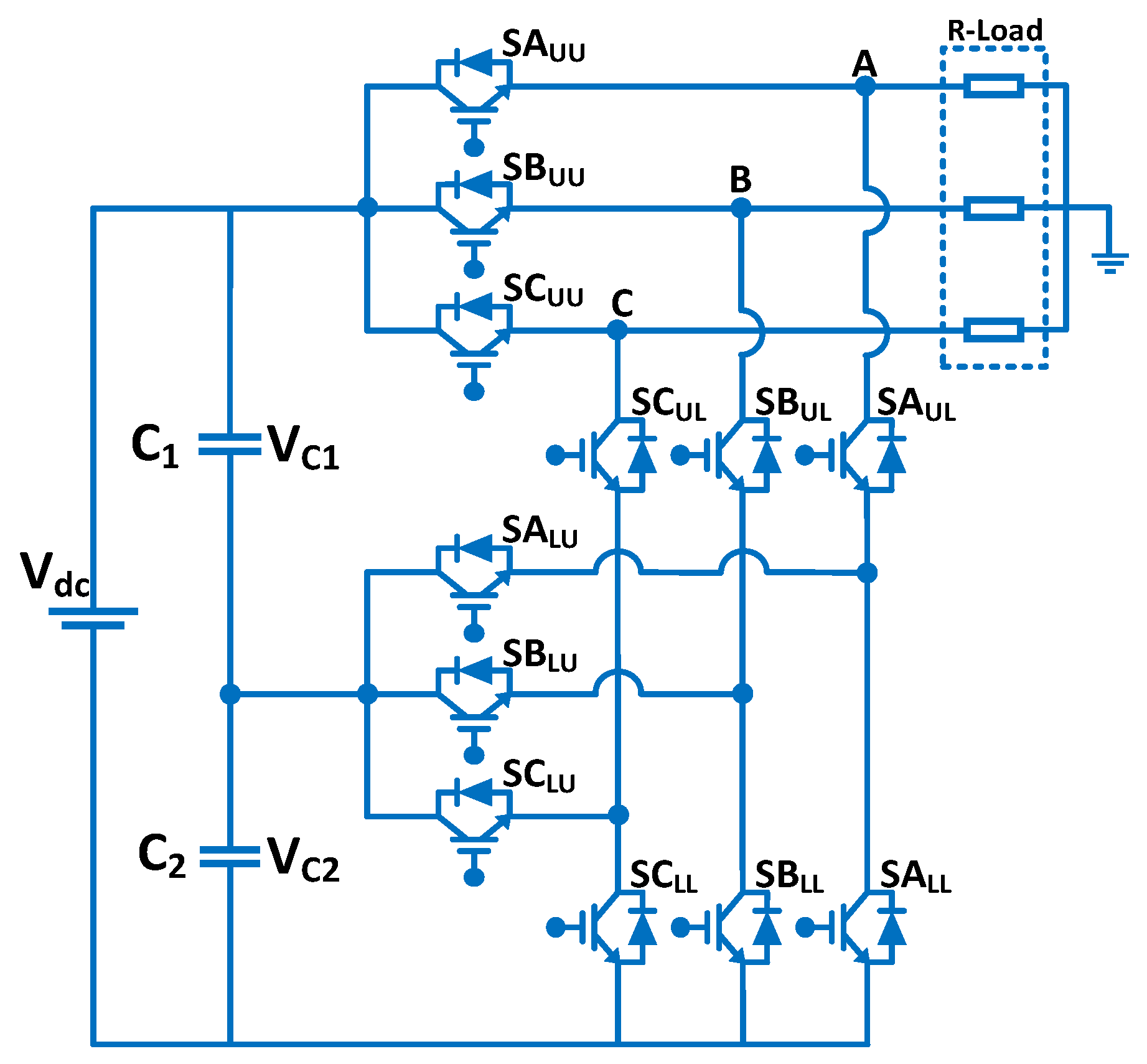
2.1. Diode-Free FT2LI Topology
2.2. Development of the SVPWM Algorithm
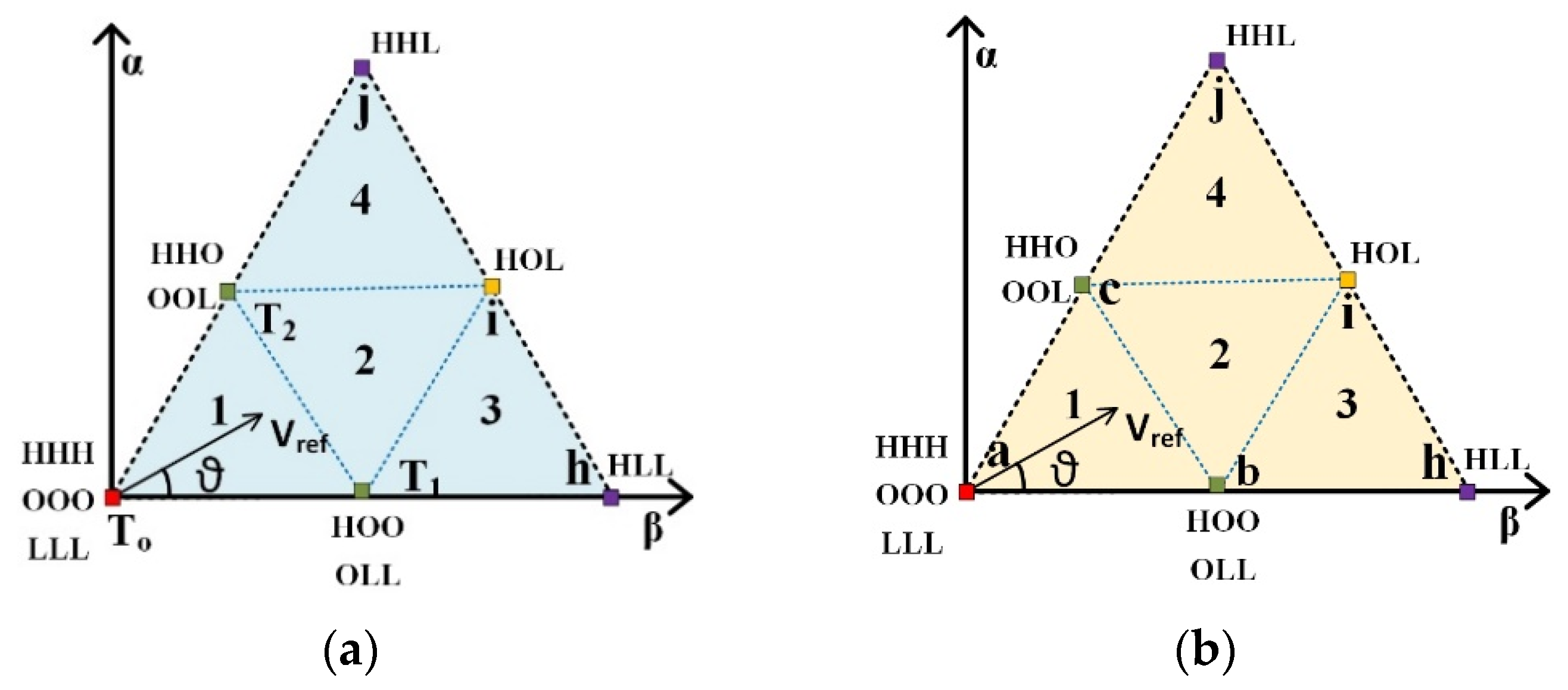
2.2.1. Sector Identification
2.2.2. Determination of Adjacent Vectors for Vref
2.2.3. Dwell Time Calculation of Each Vector
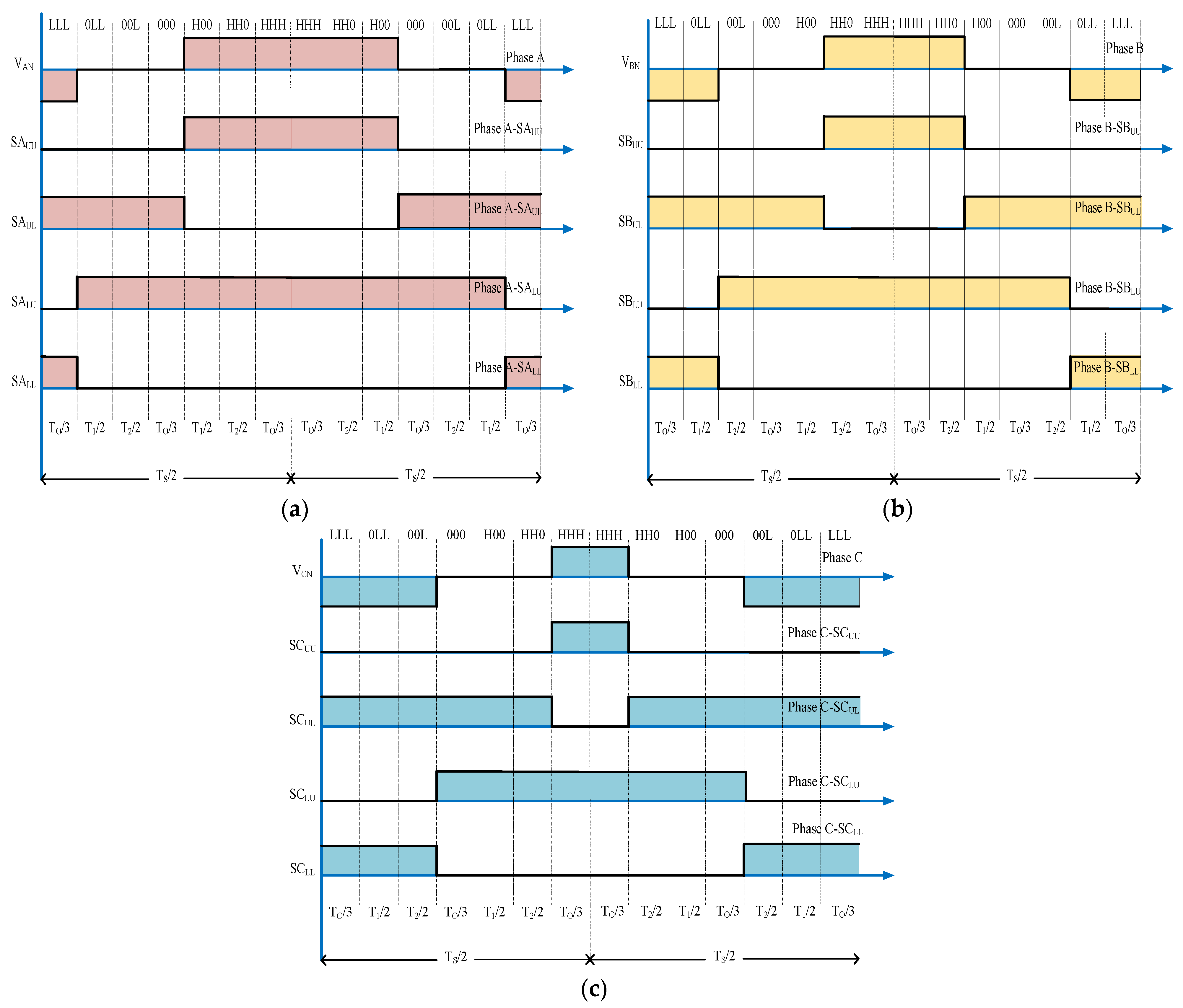
2.2.4. Selection of Redundant Vector Arrangement for a Suitable Pattern
3. Segment Reduction in SVPWM
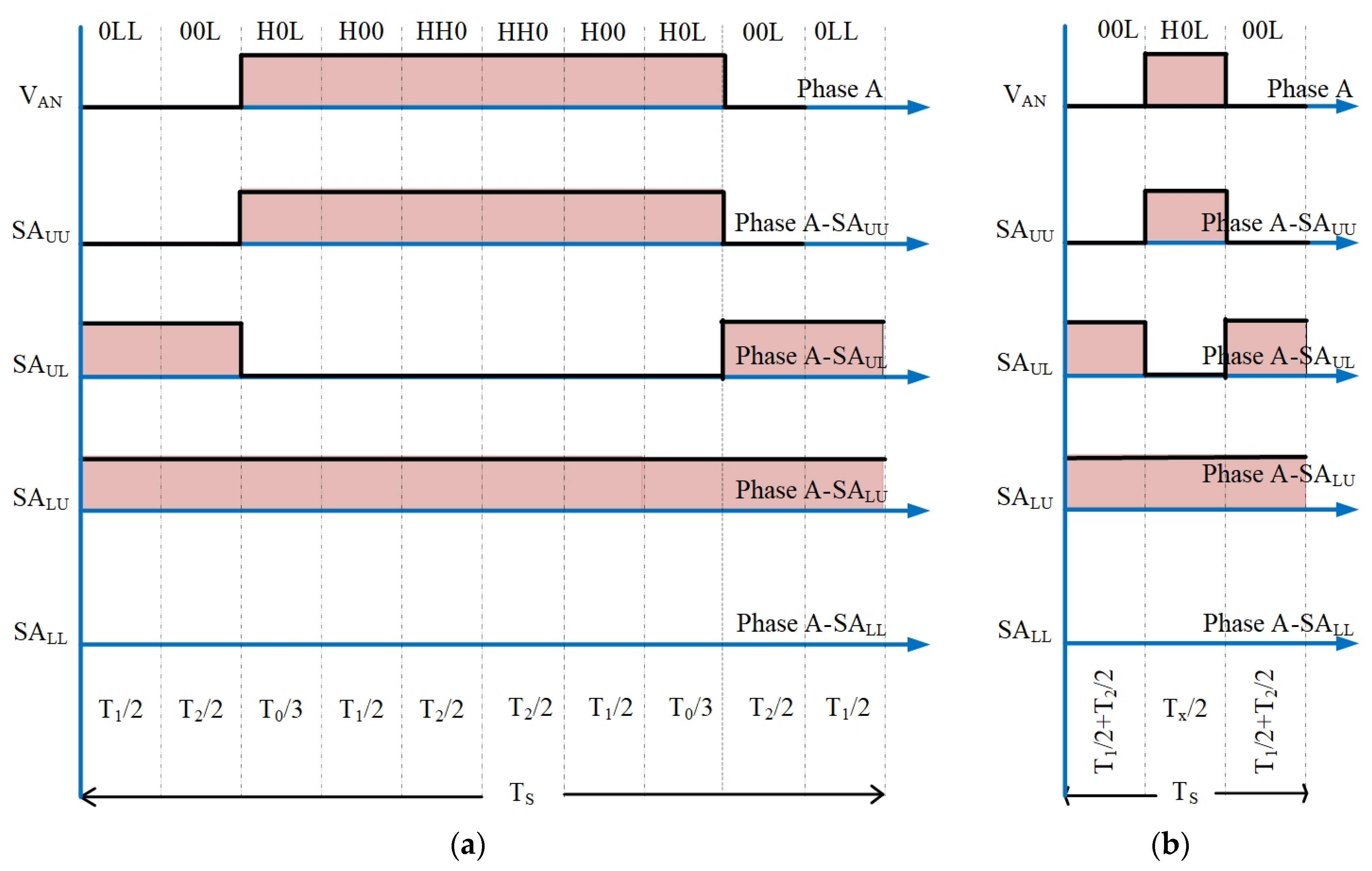
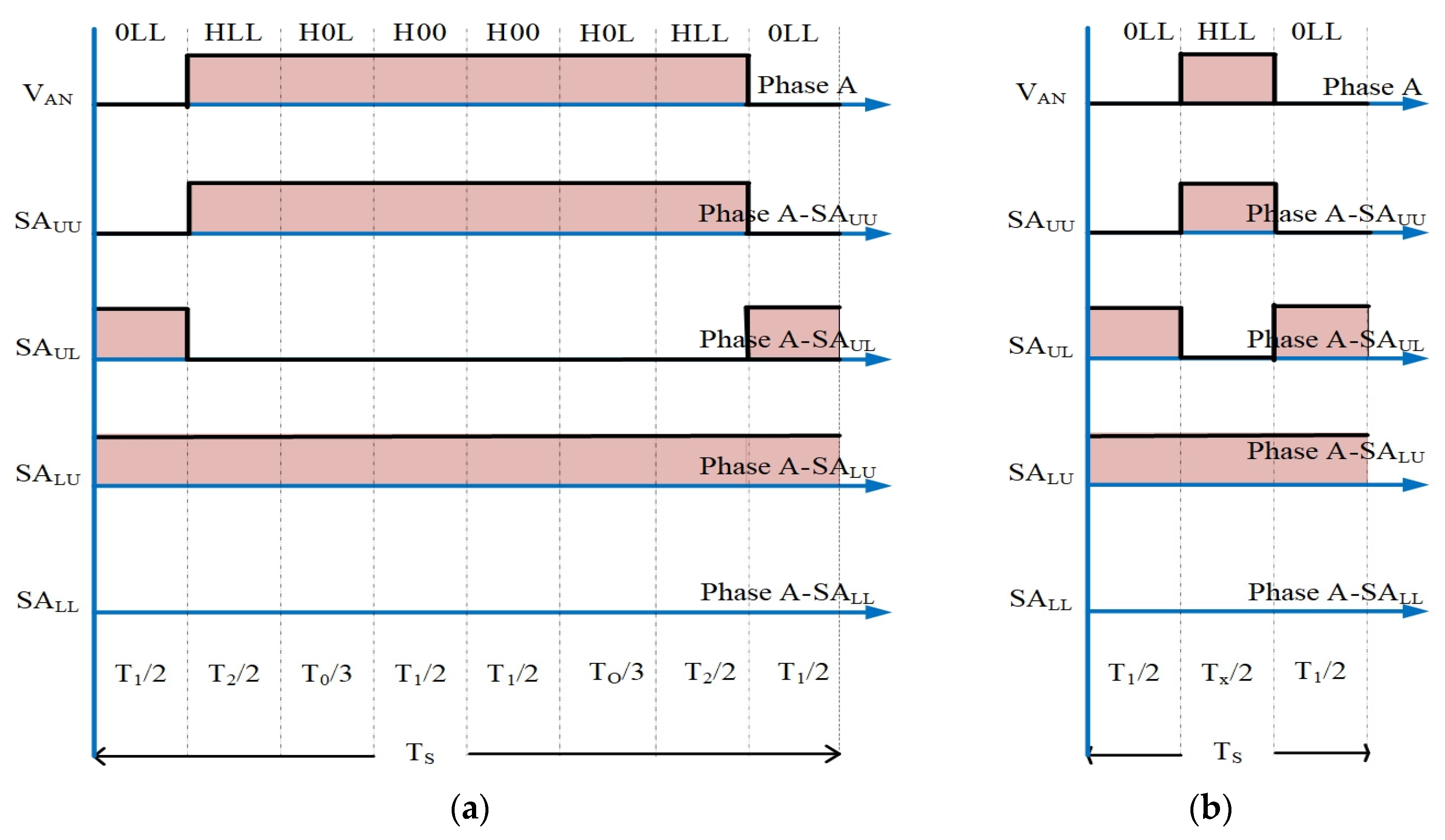
3.1. Segment Reduction in Sub-Sector 1 (Class 1)
3.2. Segment Reduction in Sub-Sector 2 (Class 2)
3.3. Segment Reduction in Sub-Sector 3 (Class 3)
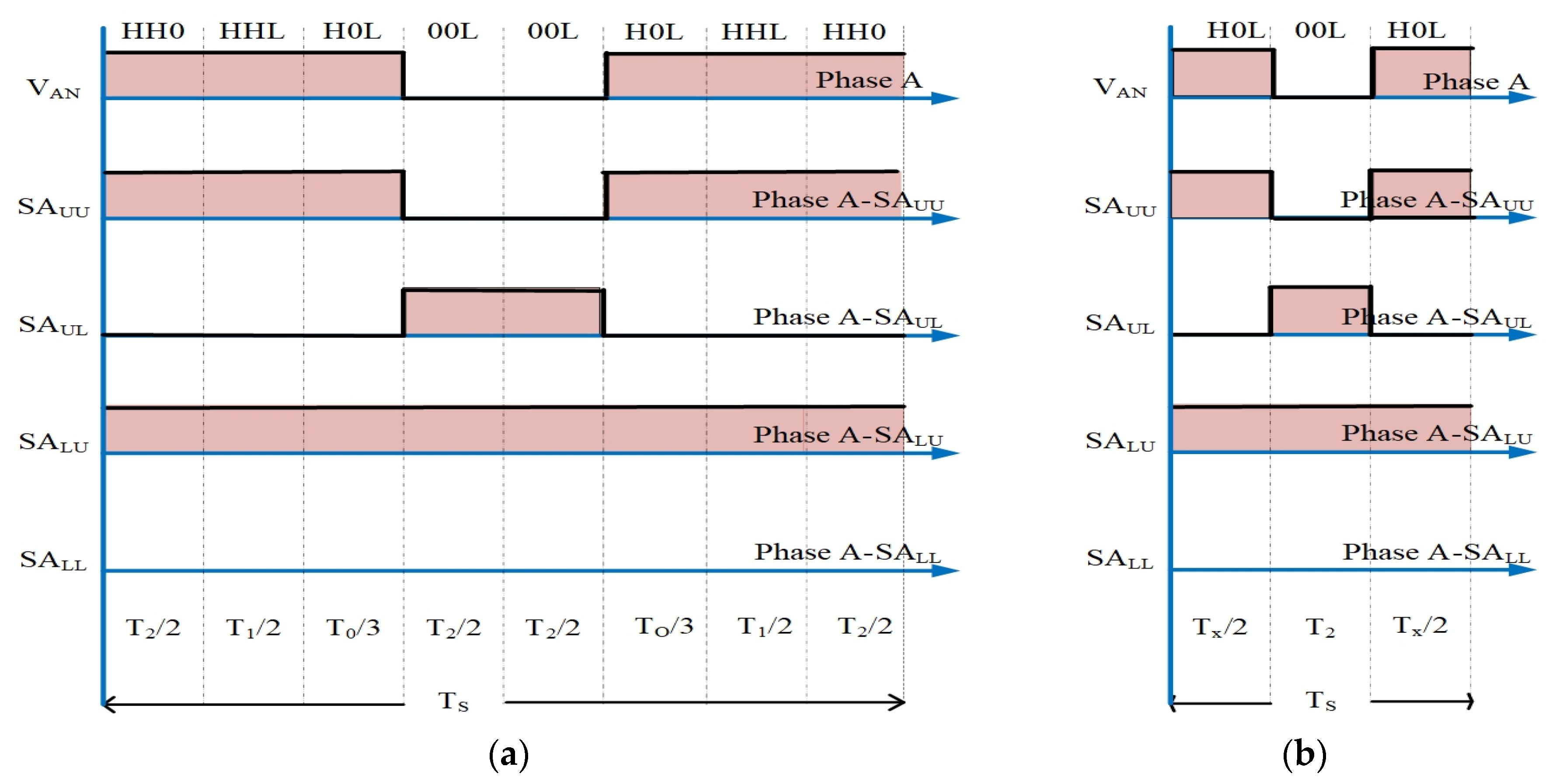
3.4. Segment Reduction in Sub-Sector 4 (Class 3)
4. Result Analysis and Discussion
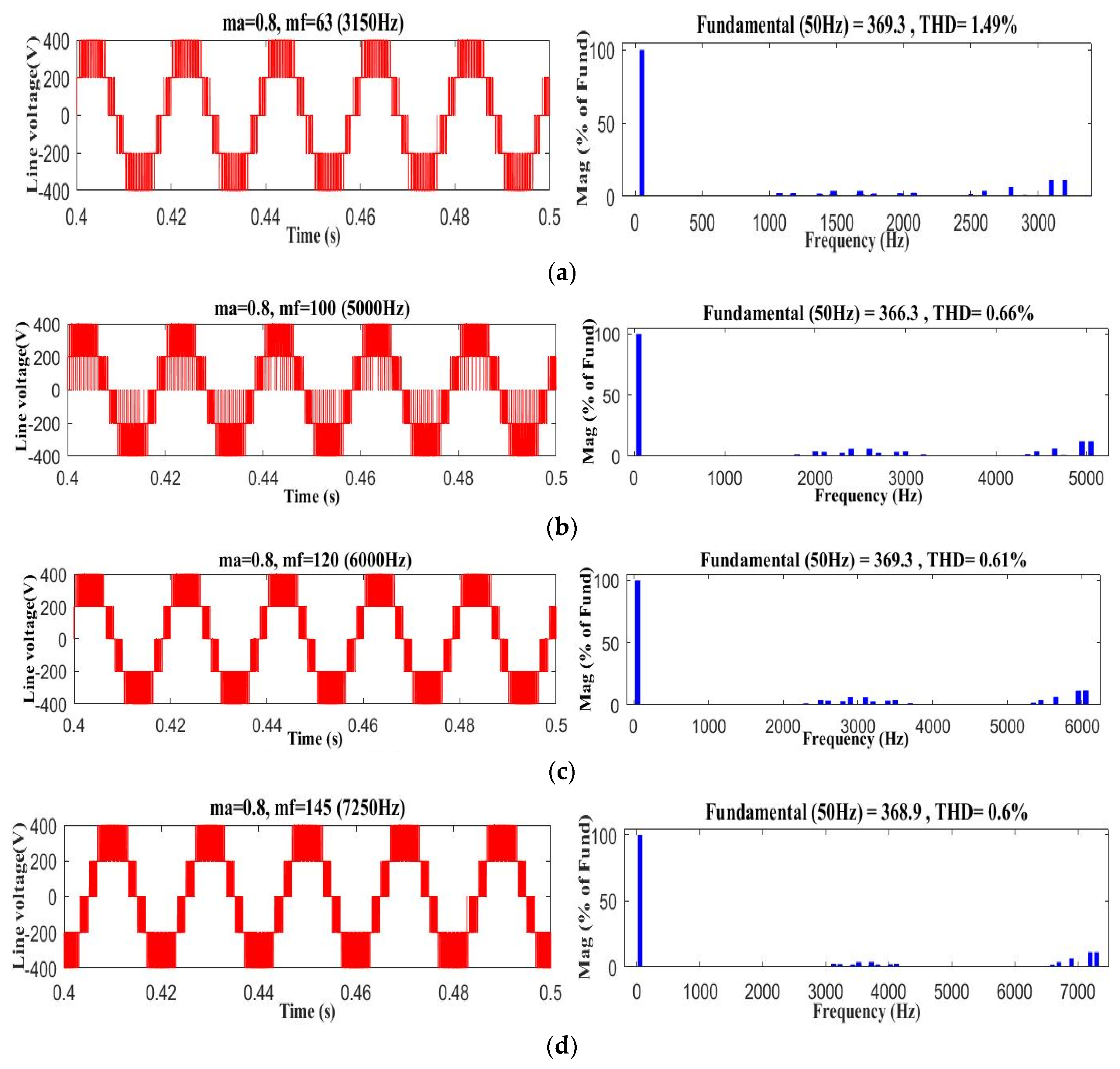
4.1. Simulation Results
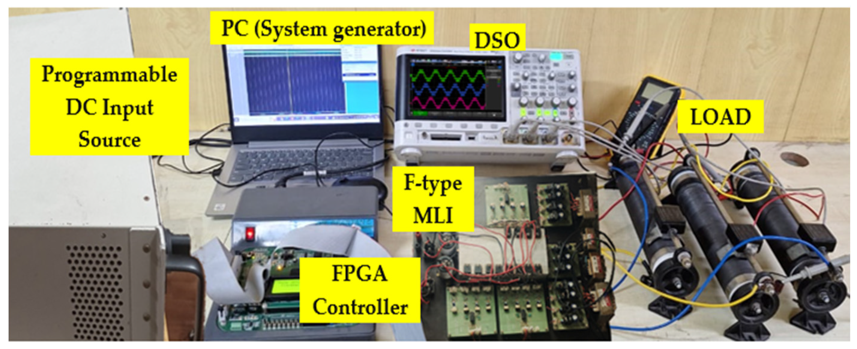
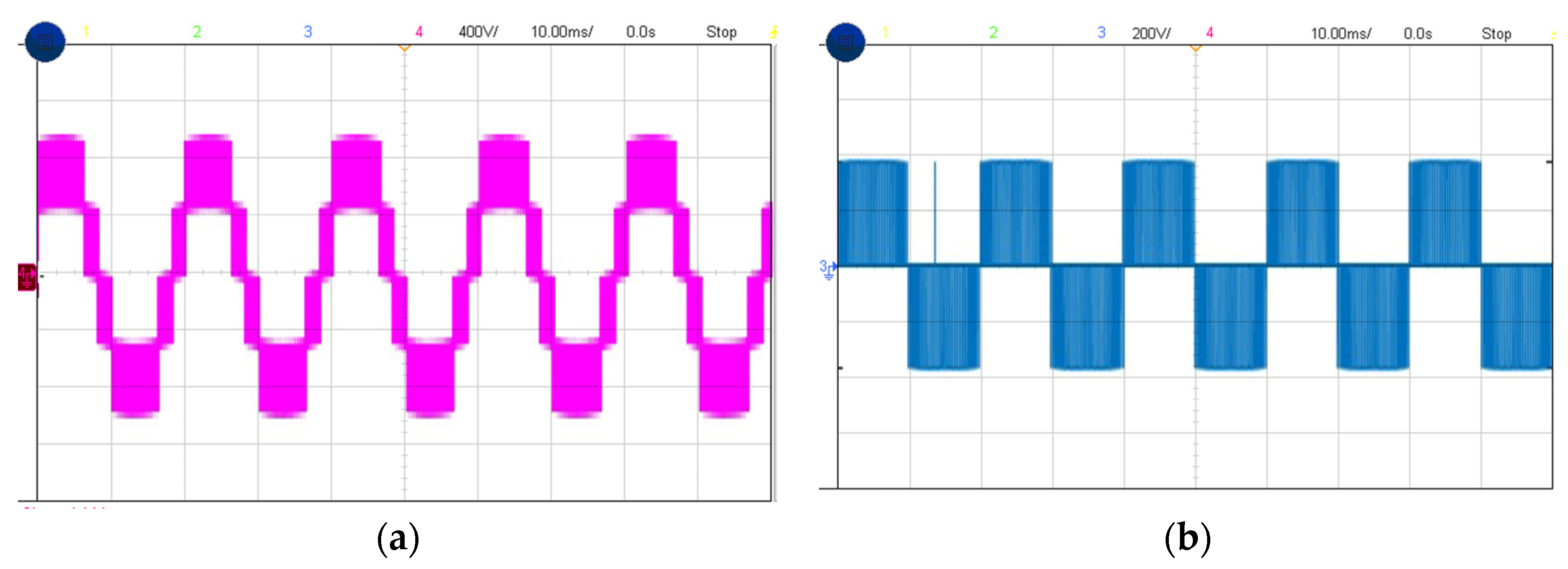
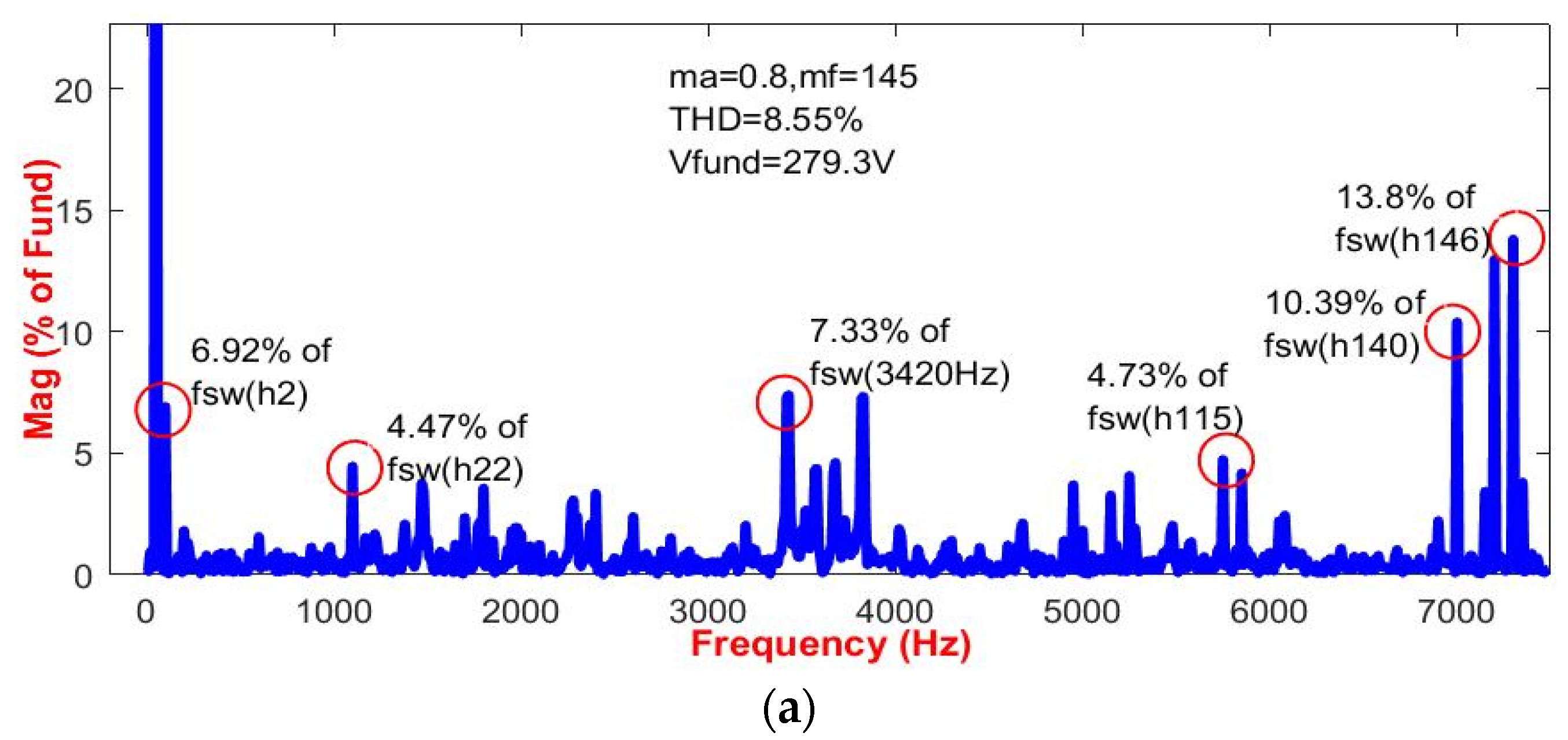
4.2. Experimental Results
5. Conclusions
Author Contributions
Funding
Data Availability Statement
Conflicts of Interest
Abbreviations
| FT2LI | F-type three-level inverter |
| SVPWM | space vector pulse width modulation |
| CBPWM | carrier-based PWM |
| MC-SPWM | multi-carrier sine PWM |
| 60° PWM | sixty-degree PWM |
| SFO PWM | switching frequency optimal PWM |
| MLIs | multilevel inverters |
References
- Rodríguez, J.; Lai, J. Multilevel Inverters: A Survey of Topologies, Controls, and Applications. IEEE Trans. Ind. Electron. 2002, 49, 724–738. [Google Scholar] [CrossRef]
- Yuan, X.; Barbi, I. Fundamentals of a New Diode Clamping Multilevel. IEEE Trans. Power Electron. 2000, 15, 711–718. [Google Scholar] [CrossRef]
- Rodriguez, J.; Bernet, S.; Steimer, P.K.; Lizama, I.E. A Survey on Neutral-Point-Clamped Inverters. IEEE Trans. Ind. Electron. 2010, 57, 2219–2230. [Google Scholar] [CrossRef]
- Cho, Y.; Labella, T.; Lai, J.; Senesky, M.K. A Carrier-Based Neutral Voltage Modulation Strategy for Multilevel Cascaded Inverters Under Unbalanced DC Sources. IEEE Trans. Ind. Electron. 2014, 61, 625–636. [Google Scholar] [CrossRef]
- Lee, T.; Li, B.; Yang, M.; Tsai, Y. A Carrier-Based PWM for Three-Level T-Type Inverter to Tolerate Open-Circuit Fault. IEEE Trans. Power Electron. 2018, 33, 8787–8796. [Google Scholar] [CrossRef]
- Pwm, C.P.; Lim, Z.; Maswood, A.I.; Ooi, G.H.P. Modular-Cell Inverter Employing Reduced Flying Capacitors with Hybrid Phase-Shifted. IEEE Trans. Ind. Electron. 2015, 62, 4086–4095. [Google Scholar] [CrossRef]
- Ghias, A.M.Y.M.; Pou, J.; Capella, G.J.; Agelidis, V.G.; Aguilera, R.P.; Meynard, T. Single-Carrier Phase-Disposition PWM Implementation for Multilevel Flying Capacitor Converters. IEEE Trans. Power Electron. 2015, 30, 5376–5380. [Google Scholar] [CrossRef]
- Li, C.; Yang, T.; Kulsangcharoen, P.; Calzo, G.L.; Bozhko, S.; Gerada, C.; Wheeler, P. A Modified Neutral-Point Balancing Space Vector Modulation for Three-Level Neutral Point Clamped Converters in High Speed Drives. IEEE Trans. Ind. Electron. 2018, 66, 910–921. [Google Scholar] [CrossRef]
- Orfanoudakis, G.I.; Yuratich, M.A.; Sharkh, S.M. Nearest-Vector Modulation Strategies with Minimum Amplitude of Low-Frequency Neutral-Point Voltage Oscillations for the Neutral-Point-Clamped Converter. IEEE Trans. Power Electron. 2013, 28, 4485–4499. [Google Scholar] [CrossRef]
- Attique, Q.M.; Li, Y.; Wang, K. A Survey on Space-Vector Pulse Width Modulation for Multilevel Inverters. CPSS Trans. Power Electron. Appl. 2017, 2, 226–236. [Google Scholar] [CrossRef]
- Deng, Y.; Teo, K.H.; Duan, C.; Habetler, T.G.; Harley, R.G. A Fast and Generalized Space Vector Modulation Scheme for Multilevel Inverters. IEEE Trans. Power Electron. 2014, 29, 5204–5217. [Google Scholar] [CrossRef]
- Al-hitmi, M.A.; Moinoddin, S.; Iqbal, A.; Rahman, K.; Meraj, M. Space Vector vs. Sinusoidal Carrier-Based Pulse Width Modulation for a Seven-Phase Voltage Source Inverter. CPSS Trans. Power Electron. Appl. 2019, 4, 230–243. [Google Scholar] [CrossRef]
- Hota, A.; Jain, S.; Agarwal, V. A Modified T-Structured Three-Level Inverter Configuration Optimized with Respect to PWM Strategy Used for Common-Mode. IEEE Trans. Ind. Appl. 2017, 53, 4779–4787. [Google Scholar] [CrossRef]
- Yao, W.; Hu, H.; Lu, Z. Comparisons of Space-Vector Modulation and Carrier-Based Modulation of Multilevel Inverter. IEEE Trans. Power Electron. 2008, 23, 45–51. [Google Scholar] [CrossRef]
- Das, S.; Narayanan, G.; Pandey, M. Space-Vector-Based Hybrid Pulsewidth Modulation Techniques for a Three-Level Inverter. IEEE Trans. Power Electron. 2014, 29, 4580–4591. [Google Scholar] [CrossRef]
- Ye, Z.; Xu, Y.; Wu, X.; Tan, G.; Deng, X.; Wang, Z. A Simplified PWM Strategy for a Converter with Unbalanced DC Links. IEEE Trans. Power Electron. 2016, 31, 3227–3238. [Google Scholar] [CrossRef]
- Inverter, M.T. An Improved Multimode Synchronized Space Vector Modulation Strategy for High-Power. IEEE Trans. Power Electron. 2021, 36, 4686–4696. [Google Scholar] [CrossRef]
- Zhang, G.; Peng, S.; Geng, Q.; Shi, T.; Xia, C. Hybrid Discontinuous Space Vector PWM Strategy. IEEE Trans. Power Electron. 2022, 37, 1711–1721. [Google Scholar] [CrossRef]
- Inverter, T.N.P.C.; Chen, F.; Qiao, W.; Wang, H.; Qu, L. A Simple Zero-Sequence Voltage Injection Method for Carrier-Based Pulsewidth Modulation of the Three-Level NPC Inverter. IEEE J. Emerg. Sel. Top. Power Electron. 2021, 9, 4687–4699. [Google Scholar] [CrossRef]
- Liu, C.; Xing, X.; Du, C.; Zhang, B.; Zhang, C.; Blaabjerg, F. An Improved Model Predictive Control Method Using Optimized Voltage Vectors for Vienna Rectifier with Fixed Switching Frequency. IEEE Trans. Power Electron. 2023, 38, 358–371. [Google Scholar] [CrossRef]
- Xiao, L.; Li, J.; Xiong, Y.; Chen, J.; Gao, H. Strategy and Implementation of Harmonic-Reduced Synchronized SVPWM for High-Power Traction Machine Drives. IEEE Trans. Power Electron. 2020, 35, 12457–12471. [Google Scholar] [CrossRef]
- Chen, Y.T.; Lin, H.T. Analysis and Implementation of a Novel Space Vector Modulation Strategy for Multilevel Inverter about the Operations in the Overmodulation Region. In Proceedings of the 2nd International Symposium on Power Electronics for Distributed Generation Systems, Hefei, China, 16–18 June 2010; pp. 417–422. [Google Scholar] [CrossRef]
- Prieto, J.; Barrero, F.; Durán, M.J.; Marín, S.T.; Perales, M.A. SVM Procedure for n -Phase VSI With Low Harmonic Distortion in the Overmodulation Region. IEEE Trans. Ind. Electron. 2014, 61, 92–97. [Google Scholar] [CrossRef]
- Song, W.; Wang, S.; Xiong, C.; Ge, X.; Feng, X. Single-phase three-level space vector pulse width modulation algorithm for grid-side railway traction converter and its relationship of carrier-based pulse width modulation. IET Electr. Syst. Transp. 2014, 4, 78–87. [Google Scholar] [CrossRef]
- Roberto, C.; Kennel, R.; Clare, J.C. A Simplified Space-Vector Modulation Algorithm for Four-Leg NPC Converters. IEEE Trans. Power Electron. 2017, 32, 8371–8380. [Google Scholar] [CrossRef]
- Inverter, S.T. Novel Switching Sequences for a Space-Vector-Modulated Three-Level Inverter. IEEE Trans. Ind. Electron. 2012, 59, 1477–1487. [Google Scholar]
- Sharma, V.; Hossain, M.J.; Mukhopadhyay, S. Fault-Tolerant Operation of Bidirectional-Fed Induction Motor Drive for Vehicular Applications. Energies 2022, 15, 6976. [Google Scholar] [CrossRef]
- Tsai, M.-F.; Tseng, C.-S.; Cheng, P.-J. Implementation of an FPGA-Based Current Control and SVPWM ASIC with Asymmetric Five-segment Switch Scheme for AC Motor Drives. Energies 2021, 14, 1462. [Google Scholar] [CrossRef]
- Odeh, C.I.; Kondratenko, D.; Lewicki, A.; Morawiec, M.; Jąderko, A.; Baran, J. Pulse-Width Modulation Template for Five-Level Switch-Clamped H-Bridge-Based Cascaded Multilevel Inverter. Energies 2021, 14, 7726. [Google Scholar] [CrossRef]
- Li, G.; Wang, L.; Li, F. Single-Phase Voltage Source Multi-Level Inverter Hysteresis SVPWM Reconfigurable Fault-Tolerant Control Method. Energies 2022, 15, 2557. [Google Scholar] [CrossRef]
- Chudzik, P.; Steczek, M.; Tatar, K. Reduction in selected Torque Harmonics in a Three level NPC Inverter fed Induction Motor Drive. Energies 2022, 15, 4078. [Google Scholar] [CrossRef]
- Tawfiq, K.B.; Ibrahim, M.N.; Sergeant, P. Power loss analysis of a Five-phase Drive system using a synchronous reluctance motor and an indirect matrix converter with reduced switching losses. Machines 2022, 10, 738. [Google Scholar] [CrossRef]
- Odeh, C.; Lewicki, A.; Morawiec, M.; Kondratenko, D. Three-Level F-Type Inverter. IEEE Trans. Power Electron. 2021, 36, 11265–11275. [Google Scholar] [CrossRef]
- Schweizer, M.; Kolar, J.W. Design and implementation of a highly efficient three-level T-type converter for low-voltage applications. IEEE Trans. Power Electron. 2013, 28, 899–907. [Google Scholar] [CrossRef]
- Zhang, L.; Sun, K.; Feng, L.; Wu, H.; Xing, Y. A family of neutral point clamped full-bridge topologies for transformerless photovoltaic grid-tied inverters. IEEE Trans. Power Electron. 2013, 28, 730–739. [Google Scholar] [CrossRef]
- Madasamy, P.; Kumar, V.S.; Sanjeevikumar, P.; Holm-Nielsen, J.B.; Hosain, E.; Bharatiraja, C. A three-phase transformerless T-Type-NPC-MLI for grid connected PV systems with common-mode leakage current mitigation. Energies 2019, 12, 2434. [Google Scholar] [CrossRef]
- Li, J.J.; Liu, J.; Boroyevich, D.; Mattavelli, P.; Xue, Y. Three-level active neutral-point-clamped zero-current-transition converter for sustainable energy systems. IEEE Trans. Power Electron. 2011, 26, 3680–3693. [Google Scholar] [CrossRef]
- Celanovic, N.; Boroyevich, D. A fast space-vector modulation algorithm for multilevel three-phase converters. IEEE Trans. Ind. Appl. 2001, 37, 637–641. [Google Scholar] [CrossRef]
- Kaarthik, R.S.; Gopakumar, K.; Cecati, C.; Nagy, I. Timing Calculations for a General N-Level Dodecagonal Space Vector Structure Using only Reference Phase Voltages. IEEE Trans. Ind. Electron. 2016, 63, 1395–1403. [Google Scholar] [CrossRef]


| On Devices/A Phase | Off Devices/A Phase | Switching States | Terminal Voltage |
|---|---|---|---|
| SAUU, SALU | SAUL, SALL | H | +Vdc/2 |
| SAUL, SALU | SAUU, SALL | O | 0 |
| SAUL, SALL | SAUU, SALU | L | −Vdc/2 |
| Parameters/Phase | PN-NPC [35] | T-Type MLI [36] | 3L-ANPC ZCT [37] | FT2LI | |
|---|---|---|---|---|---|
| Total no of switches/phase | 8 | 4 | 8 | 4 | |
| Voltage rating of switches/phase | Vdc | 2 | 2 | 6 | 1 |
| Vdc/2 | 6 | 2 | 2 | 3 | |
| No. of clamping diodes | 0 | 2 | 2 | - | |
| Auxiliary inductors | 2 | - | 1 | - | |
| Auxiliary capacitors | 1 | - | 1 | - | |
| Sector | Sub-Sector | Switching Sequence |
|---|---|---|
| 1 | I | LLL-OLL-OOL-OOO-HOO-HHO-HHH-HHH-HHO-HOO-OOO-OOL-OLL-LLL |
| II | OLL-OOL-HOL-HOO-HHO-HHO-HOO-HOL-OOL-OLL | |
| III | OLL-HLL-HOL-HOO-HOO-HOL-HLL-OLL | |
| IV | HHO-HHL-HOL-OOL-OOL-HOL-HHL-HHO | |
| 2 | I | HHH-HHO-OHO-OOO-OOL-LOL-LLL-LLL-LOL-OOL-OOO-OHO-HHO-HHH |
| II | LOL-OOL-OHL-OHO-HHO-HHO-OHO-OHL-OOL-LOL | |
| III | OOL-OHL-HHL-HHO-HHO-HHL-OHL-OOL | |
| IV | LOL-LHL-OHL-OHO-OHO-OHL-LHL-LOL | |
| 3 | I | HHH-OHH-OHO-OOO-LOO-LOL-LLL-LOL-LOO-OOO-OHO-OHH-HHH |
| II | OHH-OHO-LHO-LOO-LOL-LOL-LOO-LHO-OHO-OHH | |
| III | LOL-LHL-LHO-OHO-OHO-LHO-LHL-LOL | |
| IV | OOH-LOH-LLH-LLO-LLO-LLH-LOH-OOH | |
| 4 | I | HHH-OHH-OOH-OOO-LOO-LLO-LLL-LLL-LLO-LOO-OOO-OOH-OHH-HHH |
| II | LLO-LOO-LOH-OOH-OHH-OHH-OOH-LOH-LOO-LLO | |
| III | OHH-LHH-LOH-LOO-LOO-LOH-LHH-OHH | |
| IV | OOH-LOH-LLH-LLO-LLO-LLH-LOH-OOH | |
| 5 | I | HHH-HOH-OOH-OOO-OLO-LLO-LLL-LLL-LLO-OLO-OOO-OOH-HOH-HHH |
| II | HOH-OOH-OLH-OLO-LLO-LLO-OLO-OLH-OOH-HOH | |
| III | OOH-OLH-LLH-LLO-LLO-LLH-OLH-OOH | |
| IV | HOH-HLH-OLH-OLO-OLO-OLH-HLH-HOH | |
| 6 | I | HHH-HOH-HOO-OOO-OLO-OLL-LLL-LLL-OLL-OLO-OOO-HOO-HOH-HHH |
| II | HOH-HOO-HLO-OLO-OLL-OLL-OLO-HLO-HOO-HOH | |
| III | HOH-HLH-HLO-OLO-OLO-HLO-HLH-HOH | |
| IV | HOO-HLO-HLL-OLL-OLL-HLL-HLO-HOO |
| Switching States | Period | On Switches in Leg A | On Switches in Leg B | On Switches in Leg C | VAN | VBN | VCN | VAB | VBC | VCA | Voltage Vectors |
|---|---|---|---|---|---|---|---|---|---|---|---|
| LLL | TO/3 | SAUL SALL | SBUL SBLL | SCUL SCLL | −Vdc/2 | −Vdc/2 | −Vdc/2 | 0 | 0 | 0 | V01 = 0 |
| OLL | T1/2 | SAUL SALU | SBUL SBLL | SCUL SCLL | 0 | −Vdc/2 | −Vdc/2 | +Vdc/2 | 0 | −Vdc/2 | |
| OOL | T2/2 | SAUL SALU | SBUL SBLU | SCUL SCLL | 0 | 0 | −Vdc/2 | 0 | +Vdc/2 | −Vdc/2 | |
| OOO | TO/3 | SAUL SALU | SBUL SBLU | SCUL SCLU | 0 | 0 | 0 | 0 | 0 | 0 | V02 = 0 |
| HOO | T1/2 | SAUU SALU | SBUL SBLU | SCUL SCLU | +Vdc/2 | 0 | 0 | +Vdc/2 | 0 | −Vdc/2 | |
| HHO | T2/2 | SAUU SALU | SBUU SBLU | SCUL SCLU | +Vdc/2 | +Vdc/2 | 0 | 0 | +Vdc/2 | −Vdc/2 | |
| HHH | TO/3 | SAUU SALU | SBUU SBLU | SCUU SCLU | +Vdc/2 | +Vdc/2 | +Vdc/2 | 0 | 0 | 0 | V03 = 0 |
| Sub-Sector | To | T1 | T2 |
|---|---|---|---|
| 1 | |||
| 2 | |||
| 3 | |||
| 4 |
| Sub-Sector | Possible Switching Sequence | |
|---|---|---|
| 1 | (i) | HHH-HHO-HOO-OOO |
| (ii) | LLL-OLL-OOL-OOO | |
| (iii) | HHO-HOO-OOO-OOL | |
| (iv) | HOO-OOO-OOL-OLL | |
| 2 | (i) | HHO-HOO-HOL-OOL |
| (ii) | HOO-HOL-OOL-OLL | |
| 3 | (i) | HOO-HOL-HLL-OLL |
| 4 | (i) | HHO-HHL-HOL-OOL |
| Frequency Modulating Index (mf) | Performance Parameters | Amplitude Modulation Index (ma) | |||||
|---|---|---|---|---|---|---|---|
| Conventional SVPWM | Proposed SVPWM | ||||||
| 0.7 | 0.8 | 0.9 | 0.7 | 0.8 | 0.9 | ||
| ODD and TRIPLEN mf = 3150/50 = 63 | THD | 4.55 | 4.81 | 6.32 | 1.11 | 1.49 | 2.66 |
| VFund | 302.55 | 344.1 | 379.33 | 323.2 | 369.3 | 410 | |
| VRMS | 213.9 | 243.3 | 268.2 | 228.5 | 261.2 | 289.9 | |
| EVEN and NON TRIPLEN mf = 5000/50 = 100 | THD | 3.42 | 3.05 | 2.82 | 0.79 | 0.66 | 1.96 |
| VFund | 301.9 | 349.8 | 394.5 | 321.9 | 366.3 | 406.8 | |
| VRMS | 213.5 | 247.38 | 278.99 | 227.6 | 259 | 287.6 | |
| EVEN and TRIPLEN mf = 6000/50 = 120 | THD | 3.57 | 1.08 | 0.75 | 0.67 | 0.61 | 1.58 |
| VFund | 318.8 | 365.57 | 401.37 | 323.4 | 369.3 | 410 | |
| VRMS | 225.45 | 258.53 | 283.59 | 228.7 | 261.3 | 289.9 | |
| ODD and NON TRIPLEN mf = 7250/50 = 145 | THD | 3.93 | 0.95 | 0.73 | 0.79 | 0.6 | 1.59 |
| VFund | 310.6 | 341.57 | 399.43 | 323.1 | 368.9 | 410.1 | |
| VRMS | 219.66 | 241.56 | 282.48 | 228.5 | 260.1 | 290 | |
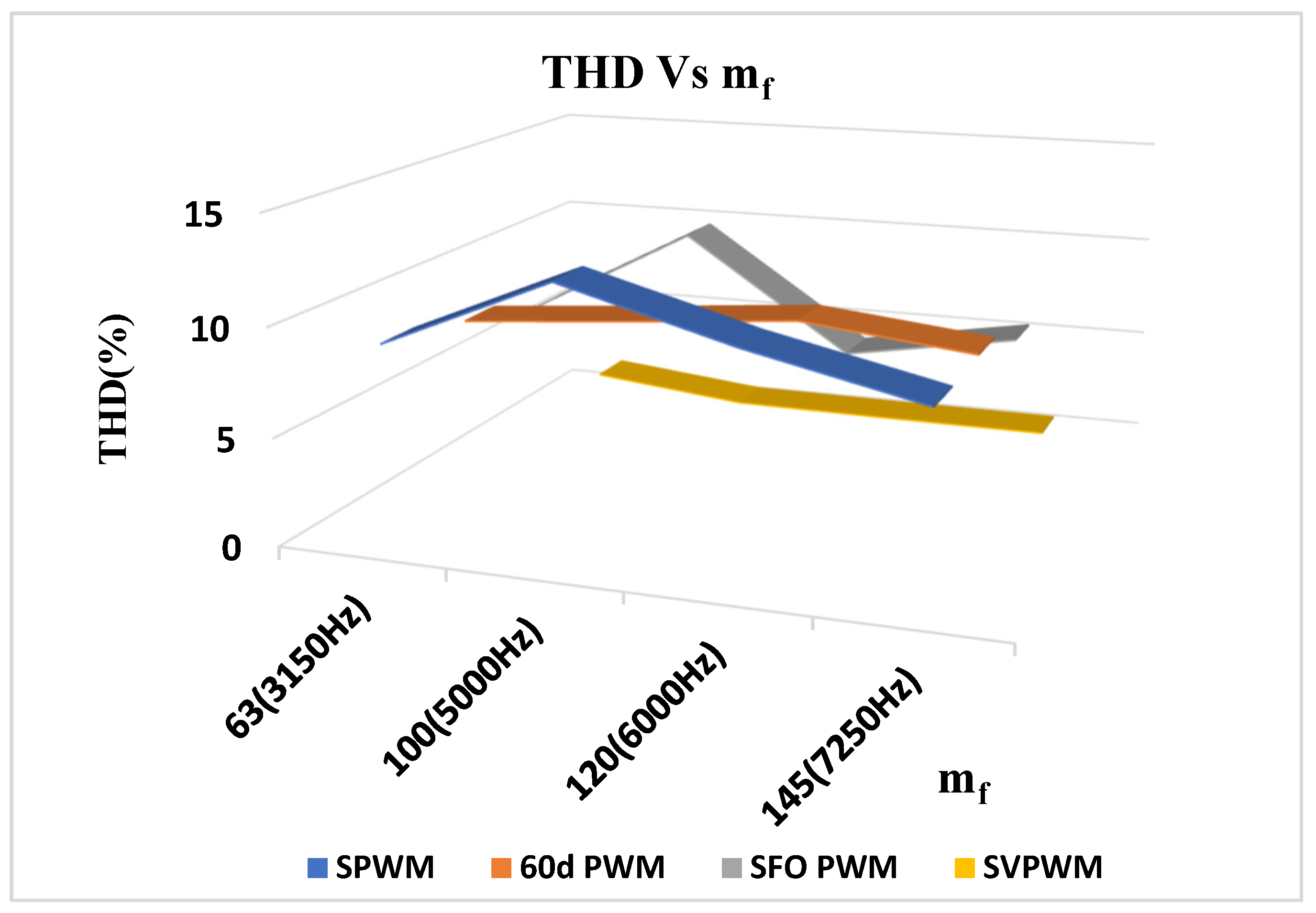
| Frequency Modulation Index (mf) | Performance Parameters | Amplitude Modulation Index (ma) | |||||||||||
|---|---|---|---|---|---|---|---|---|---|---|---|---|---|
| MC-SPWM | MC-60° PWM | MC-SFO PWM | Proposed SVPWM | ||||||||||
| 0.7 | 0.8 | 0.9 | 0.7 | 0.8 | 0.9 | 0.7 | 0.8 | 0.9 | 0.7 | 0.8 | 0.9 | ||
| Odd and Triplen mf = 3150/50 = 63 | THD | 9.41 | 9.02 | 8.36 | 8.67 | 8.21 | 8.59 | 7.66 | 7.12 | 6.04 | 1.11 | 1.49 | 2.66 |
| VFund | 235 | 276.4 | 311.2 | 266.4 | 297.7 | 340.9 | 279.6 | 318.5 | 360.6 | 323.2 | 369.3 | 410 | |
| VRMS | 166.2 | 195.4 | 220 | 188.3 | 210.5 | 241.1 | 197.7 | 225.2 | 255 | 228.5 | 261.2 | 289.9 | |
| Even and Non Triplen mf = 5000/50 = 100 | THD | 11.52 | 12.41 | 9.12 | 11.03 | 8.86 | 6.49 | 7.08 | 11.37 | 6.01 | 0.79 | 0.66 | 1.96 |
| VFund | 235 | 284.1 | 310.4 | 245.2 | 318.7 | 336.6 | 263.2 | 332 | 362.1 | 321.9 | 366.3 | 406.8 | |
| VRMS | 166.2 | 200.9 | 219.5 | 173.4 | 225.3 | 238 | 186.1 | 234.8 | 256 | 227.6 | 259 | 287.6 | |
| Even and Triplen mf = 6000/50 = 120 | THD | 9.86 | 10.28 | 8.75 | 9.27 | 9.56 | 8.31 | 6.88 | 6.09 | 6.48 | 0.67 | 0.61 | 1.58 |
| VFund | 242.2 | 276.7 | 311.3 | 262.4 | 299 | 339.3 | 280.6 | 320.6 | 360.5 | 323.4 | 369.3 | 410 | |
| VRMS | 171.5 | 195.6 | 220.1 | 185.5 | 211.5 | 239.9 | 198.4 | 226.7 | 254.9 | 228.7 | 261.3 | 289.9 | |
| Odd and Non Triplen mf = 7250/50 = 145 | THD | 8.84 | 8.55 | 8.03 | 9.36 | 8.72 | 8.35 | 8.15 | 7.46 | 6.83 | 0.79 | 0.6 | 1.59 |
| VFund | 240.4 | 279.3 | 311.4 | 262.3 | 301.3 | 338.6 | 281.2 | 319.5 | 360.5 | 323.1 | 368.9 | 410.1 | |
| VRMS | 170 | 197.5 | 220.2 | 185.5 | 213.1 | 239.4 | 198.2 | 225.9 | 254.9 | 228.5 | 260.1 | 290 | |
| Inverter Specification | [3] | [13] | [15] | [25] | [29] | SVPWM-Based FT2LI |
|---|---|---|---|---|---|---|
| Voltage rating required for switches | Vdc | Vdc | Vdc | Vdc | Vdc | Vdc(SUU) Vdc/2(SUL,SLU,SLL) |
| Active switches/switching period | 6 | 5 | 4 | 4 | 4 | 4 |
| No of clamping diodes/leg | - | - | 2 | 2 | 2 | - |
| No of DC voltage sources | Vdc | 4 Vdc | Vdc | Vdc | Vdc | Vdc |
| No of capacitors | 2 | 4 | 2 | 2 | 2 | 2 |
| Switching method applied | Basic modulation method | Zero common mode voltage SV method | Space vector-based hybrid PWM | Minimum switching transition principle | Double switching clamping sequence | Segment reduction Technique |
| Filter requirement | Medium | Low | Medium | Low | Medium | Low |
| Even harmonic elimination | Not applied | Not applied | Not applied | Applied | Not applied | Applied |
Disclaimer/Publisher’s Note: The statements, opinions and data contained in all publications are solely those of the individual author(s) and contributor(s) and not of MDPI and/or the editor(s). MDPI and/or the editor(s) disclaim responsibility for any injury to people or property resulting from any ideas, methods, instructions or products referred to in the content. |
© 2023 by the authors. Licensee MDPI, Basel, Switzerland. This article is an open access article distributed under the terms and conditions of the Creative Commons Attribution (CC BY) license (https://creativecommons.org/licenses/by/4.0/).
Share and Cite
Madhavan, M.; Nallaperumal, C.; Hossain, M.J. Segment Reduction-Based Space Vector Pulse Width Modulation for a Three-Phase F-Type Multilevel Inverter with Reduced Harmonics and Switching States. Electronics 2023, 12, 4035. https://doi.org/10.3390/electronics12194035
Madhavan M, Nallaperumal C, Hossain MJ. Segment Reduction-Based Space Vector Pulse Width Modulation for a Three-Phase F-Type Multilevel Inverter with Reduced Harmonics and Switching States. Electronics. 2023; 12(19):4035. https://doi.org/10.3390/electronics12194035
Chicago/Turabian StyleMadhavan, Meenakshi, Chellammal Nallaperumal, and Md. Jahangir Hossain. 2023. "Segment Reduction-Based Space Vector Pulse Width Modulation for a Three-Phase F-Type Multilevel Inverter with Reduced Harmonics and Switching States" Electronics 12, no. 19: 4035. https://doi.org/10.3390/electronics12194035
APA StyleMadhavan, M., Nallaperumal, C., & Hossain, M. J. (2023). Segment Reduction-Based Space Vector Pulse Width Modulation for a Three-Phase F-Type Multilevel Inverter with Reduced Harmonics and Switching States. Electronics, 12(19), 4035. https://doi.org/10.3390/electronics12194035