Article

A Family of Five-Level Pseudo-Totem Pole Dual Boost Converters

1
School of Electrical Engineering, China Shenyang University of Technology, Shenyang 110870, China
2
State Gird Henan Anyang Power Supply Co., Ltd., Anyang 455000, China
3
College of Electrical Engineering and New Energy, China Three Gorges University, Yichang 443002, China
*
Authors to whom correspondence should be addressed.
Electronics 2023, 12(17), 3722; https://doi.org/10.3390/electronics12173722
Submission received: 25 May 2023 / Revised: 30 August 2023 / Accepted: 31 August 2023 / Published: 3 September 2023

Abstract

:
In this paper, based on the pseudo-totem pole (PTP) circuit, a family of five-level PTP dual boost converters (PDBC) is proposed. A dual boost converter has some unique advantages, such as having no risk of bridge arm shoot-through and no problems related to switch body diode reverse recovery; thus, it has a good potential for applications. First, the derivation process, working principle, modulation and strategy of the topology are analyzed. Further, the number of power devices, switch voltages and current stress of the proposed topology is analyzed. Finally, a representative five-level PDBC experimental prototype is designed with AC input 220 V/50 Hz, DC output 400 V/1 kW, and peak efficiency of 98.27%. The experimental results show that the five-level PDBC proposed in this paper has higher efficiency and the correctness of its topology is verified.

1. Introduction

With the development of power electronics technology, the neutral point clamped (NPC) multi-level converter has attracted more and more scholars’ attention [1,2]. Multi-level NPC converters have the advantages of high efficiency, high power density, low total harmonic distortion (THD) and low voltage and current stress [3,4,5]. Therefore, multi-level NPC converters are widely used in medium and high power, medium voltage applications [6,7,8,9], such as electric vehicles (EVs), motor drives, electrical railway traction, and DC-bus microgrids [10,11,12,13].
Compared to an IGBT, a power MOSFET has some excellent characteristics, such as high frequency operation andlow switching and conduction losses. Therefore, power MOSFETs are widely used in low-power converters to improve efficiency and reduce volume. However, due to the poor reverse recovery characteristics of the body diode, those that are MOSFET-based have a risk of device failure, which is related to the phase-leg shoot, and this may cause false triggering of the gate voltage. Therefore, conventional H-bridge converters often use IGBTs [14,15,16,17]. The dual boost/buck converter can avoid the shoot-through problem effectively, and the freewheeling current flows through the independent diode to resolve the MOSFET body diode reverse recovery problem [14,15,16,17,18,19,20,21]. However, due to the two inductance structures of the dual boost/buck converter, the volume and weight of the converter will increase. With this in mind, the multi-level dual boost/buck converter has been proposed in [16,17,22], to reduce the size and weight of this type of topology.
The bridgeless converter has a high power factor (PF), low THD and high efficiency. This type includes the basic bridgeless converters, bidirectional-switch bridgeless converters, totem pole bridgeless converters and PTP bridgeless converters [22,23,24]. Among these, the PTP bridgeless converter has a simple structure, few semiconductor devices conducting in the series loop and a natural dual-boost structure. In order to increase the power density and reduce the THD, the PTP bridgeless converter must work at a higher frequency. Moreover, all the active devices in the circuit carry a DC voltage, which causes high voltage stress [3].
Figure 1 shows two common five-level converter topologies. Figure 1a is conventional five-level converter (CFLC), which is widely used in bidirectional power flow scenarios such as vehicle to grid (V2G) technologies. However, the number of switches is large; thus, this can be further optimized to reduce the number of switches. Figure 1b is a unidirectional five-level converter proposed in [25], which uses only one NPC bridge arm in the CFLC to reduce the number of switches. However, there is no topology derivation process. In [4], a new five-level converter with high power density is proposed and the current stress is analyzed; however, the number of active devices is large, and the cost is high. In [14,16], the PTP bridgeless structure is adopted to achieve a five-level, dual-buck, grid-connected inverter, and these papers summarize a topology structure method to expand the circuit. However, the utilization of these two input inductors is low.
Based on the above analysis, the bridge arm of the topology proposed in [25] is used as the prototype to obtain new five-level bridge arms. By cascading the five-level bridge arms with the three-level PTP circuit, a family of five-level PDBCs is proposed. The proposed PDBC optimizes the three-level PTP converter to address the large volume and large switching losses and to retain the dual boost structure; thus, it has high reliability.
The structure of this paper is as follows. Section 2 derives the PDBC in detail and analyzes the working principle. Section 3 designs the control and modulation strategy of PDBC. In Section 4, the voltage and current stress are analyzed. Section 5 conducts experimental verification on PDBC. Finally, Section 6 concludes the paper.

2. Topological Derivation and Operating Principle

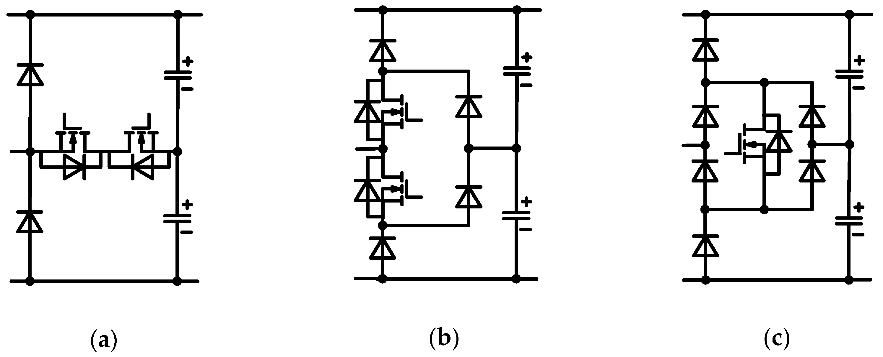
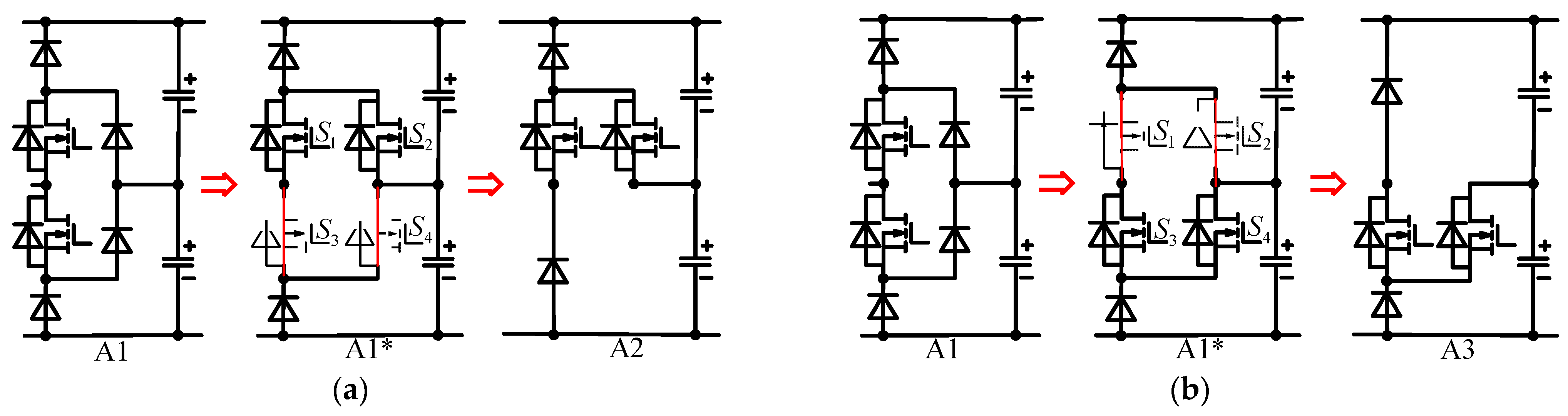
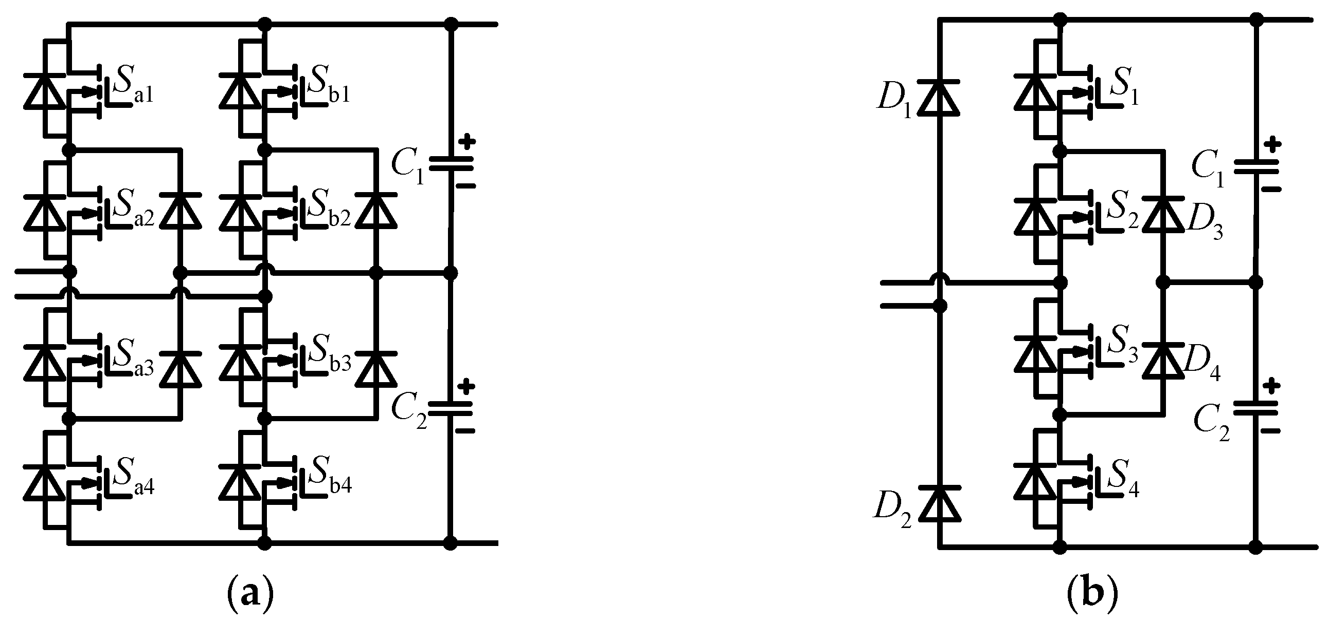
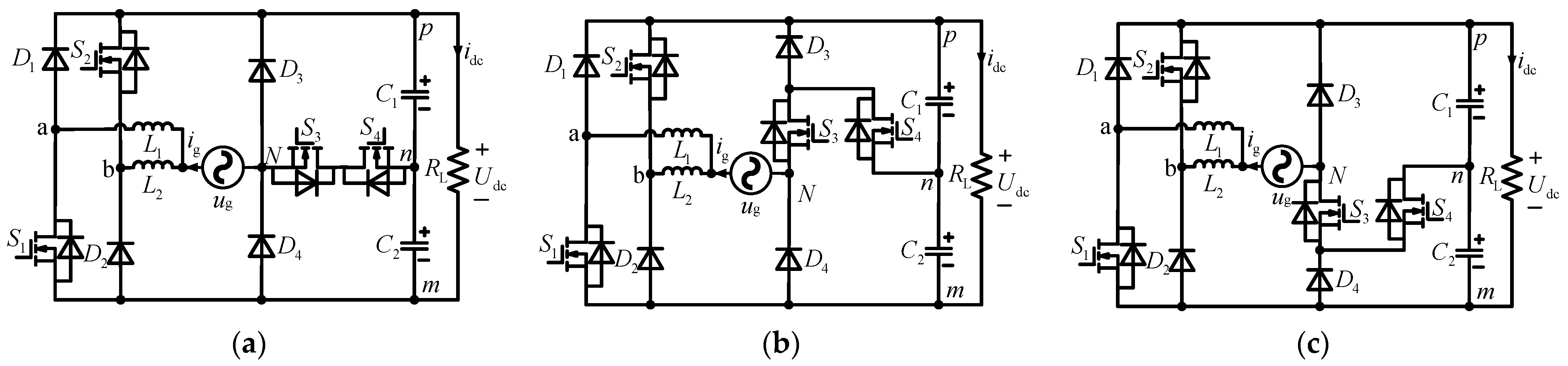
2.1. Topological Derivation

Figure 2 shows the three most commonly used clamping bridge arm structures in five-level converters. A new five-level converter can be obtained by cascading these three clamping bridge arm structures with a three-level circuit.
In this paper, the bridge arm shown in Figure 2b is used to generate a new bridge arm, as shown in Figure 3. For ease of description, the bridge arms are numbered below each bridge arms, i.e., A1, A2. Firstly, the two diodes on the right side of A4 are replaced with MOSFETs to get A1*. Then, S2 and S4 of A1* are removed and reconnected to get a new bridge arm A2, as shown in Figure 3a. In the same way, S1 and S3 of A1* are removed and reconnected to obtain a new bridge arm, A3, as shown in Figure 3b.
Through the bridge arm transformation in Figure 3, new bridge arms A2 and A3 are derived. Figure 4 shows a family of five-level PTP dual boost converters, which are named as PDBC-I, PDBC-II and PDBC-III. It can be seen in Figure 4 that the PTP dual boost converter is cascaded with Figure 2a, A2, and A3 to generate the PDBCs.
Compared to the traditional five-level converter, a family of PDBCs proposed in this paper reduces the number of MOSFETs by four, so it can effectively reduce the converter loss. It is worth mentioning that the three power flow converters proposed in this paper can all achieve bidirectional power flow after a slight circuit modification.

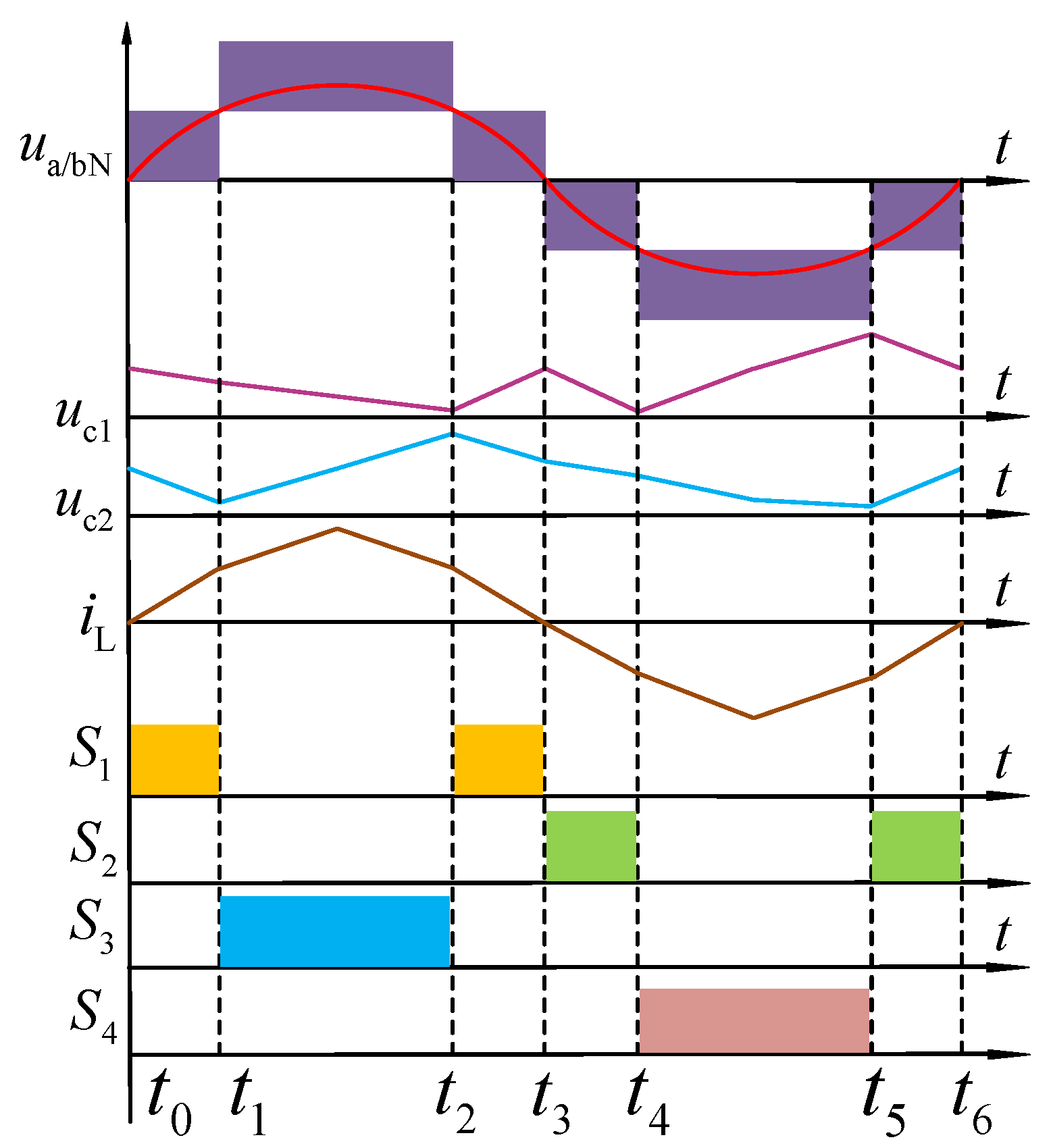
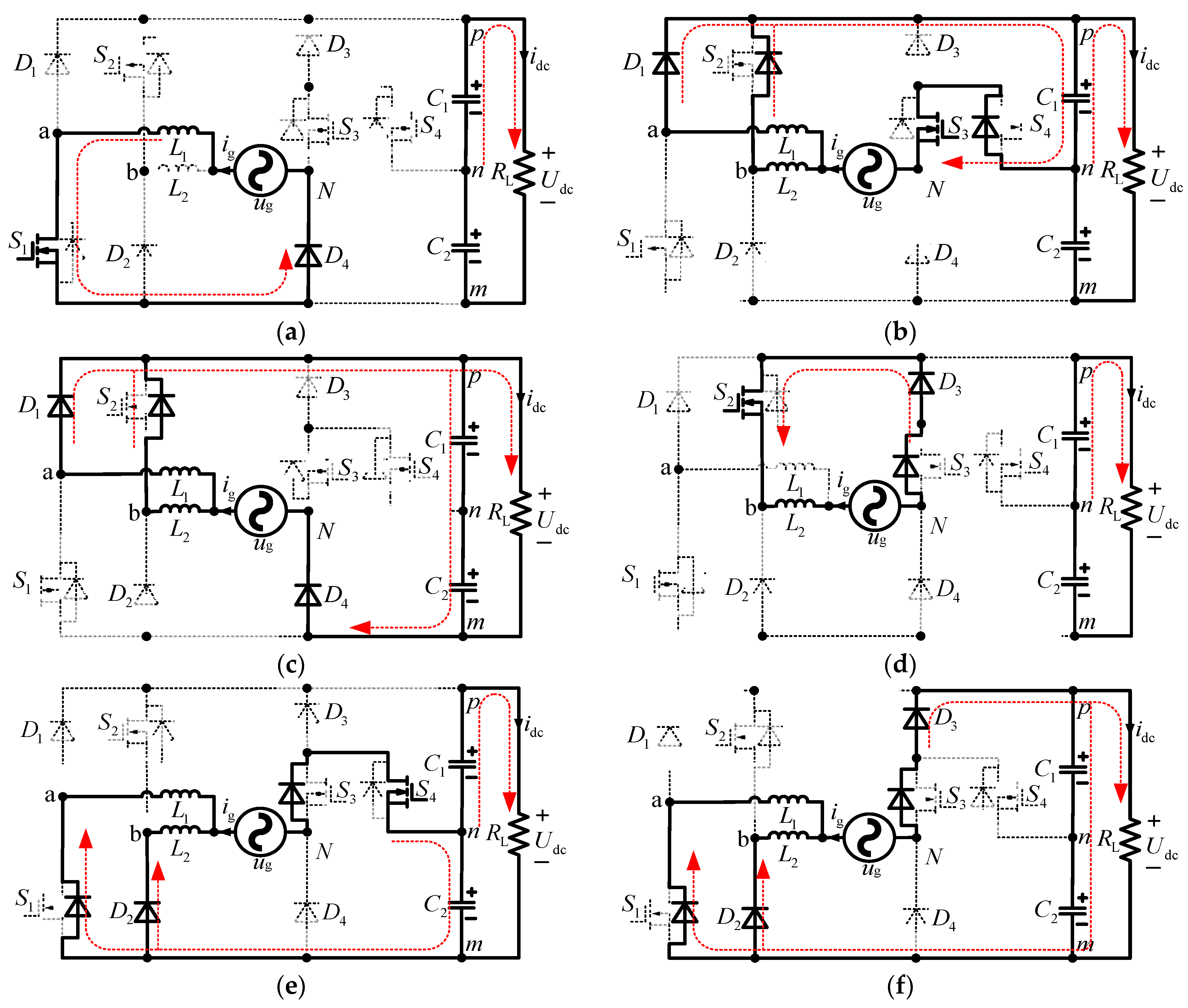
2.2. Operating Principle

Based on the above analysis, this paper uses the PDBC-II as an example for the working mode analysis. Figure 5 shows the key waveforms of one power cycle, which are corresponding to the six working modes in Figure 6. For ease of analysis, it is assumed that the circuit works in continuous conduction mode (CCM), the inductances and capacitors are large enough, the capacitor voltage UC1 = UC2 = Udc/2 and the DC voltage, Udc, remains constant. Figure 6 shows the six working modes of PDBC-II, which correspond to 0, ±0.5Udc and ±Udc. The six working modes are analyzed as follows.
In Working mode 1, during [t0, t1] shown in Figure 5, the grid voltages are ug > 0, uaN = 0 and ubN = ug. In this mode, the current path is shown in Figure 6a. As shown in Figure 6a, the switch S1 is ON, the diode D4 is ON and the other active components are OFF. The capacitors C1 and C2 are discharging to the load RL.
In Working mode 2, during [t1, t2] shown in Figure 5, the grid voltages are ug > 0 and uaN = ubN = Udc/2. In this mode, the current path is shown in Figure 6b. As shown in Figure 6b, the switch S3 is ON, the body diodes of S2 and S4 are ON, the diode D1 is ON and the other active components are OFF. The capacitor C1 is charging and C2 is discharging to the load RL.
In Working mode 3, during [t2, t3] shown in Figure 5, the grid voltages are ug > 0 and uaN = ubN = Udc. In this mode, the current path is shown in Figure 6c. As shown in Figure 6c, the body diode of S2 is ON, the diodes D1 and D4 are ON and the other active components are OFF. The capacitors C1 and C2 are charging, and the AC power supplies to the load RL.
In Working mode 4, during [t3, t4] shown in Figure 5, the grid voltages are ug < 0, ubN = ug and ubN = 0. In this mode, the current path is shown in Figure 6d. As shown in Figure 6d, the switch S2 is ON, the body diode of S3 is ON, the diode D3 is ON and the other active components are OFF. The capacitors C1 and C2 are discharging to the load RL.
In Working mode 5, during [t4, t5] shown in Figure 5, the grid voltage ug < 0 and uaN = ubN = −Udc/2. In this mode, the current path is shown in Figure 6e. As shown in Figure 6e, the switch S4 is ON, the body diodes of S1 and S3 are ON, the diode D2 is ON and the other active components are OFF. The capacitor C2 is charging and C1 is discharging to the load RL.
In Working mode 6, during [t5, t6] shown in Figure 5, the grid voltages are ug < 0 and uaN = ubN = −Udc. In this mode, the current path is shown in Figure 6f. As shown in Figure 6f, the body diodes of S1 and S3 are ON, the diodes D2 and D3 are ON, and the other active components are OFF. The capacitors C1 and C2 are charging, and the AC power supplies to the load RL.
Based on the six working mode analyses above, the switching pulse distribution of the PDBC-II is summarized in Table 1. Where “0” and “1” represent switching off and on, “↑” and “↓” represent capacitor charging and discharging, respectively. It can be seen from Table 1 that the PDBC-II has at most one switch ON in each mode, so the PDBC-II has a lower conduction loss.

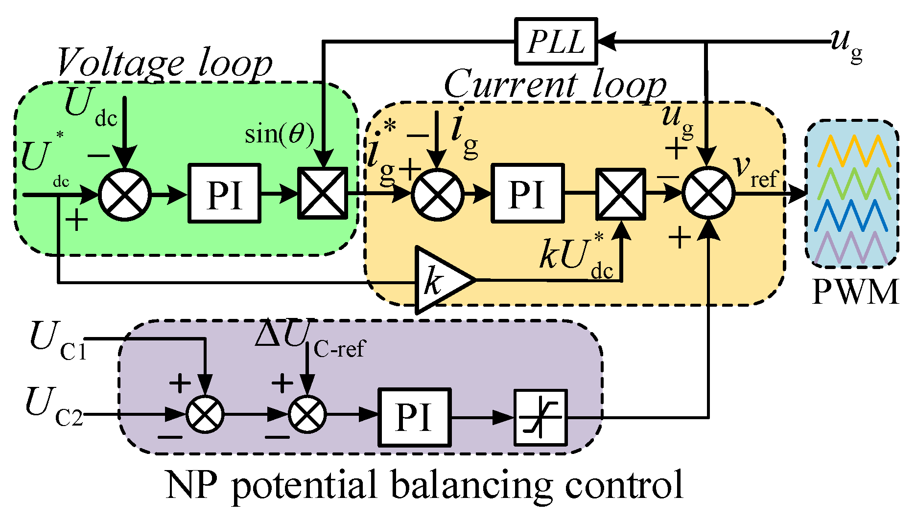
3. Control and Modulation Strategy

3.1. Control Strategy

In this paper, a double closed-loop control system suited for PDBCs is designed; both the voltage outer loop and the current inner loop adopt the PI controller. The control block diagram of the PDBCs is shown in Figure 7. The transfer function of the PI link in Figure 7 can be expressed as Equation (1),
G pi = ( k p s + k i ) / s ,
where kp and ki are the proportional and integral coefficients, respectively.
The voltage outer loop is used to keep the output voltage Udc stable; this output is the reference value of the current inner loop. Firstly, the difference between the DC side voltage, Udc, and its reference value, Udc*, is sent into the PI controller to obtain an error signal. Then, the error signal is multiplied by the phase information of the grid voltage ug. As a result, the input reference signal, ig*, of the current inner loop is obtained.
The current inner loop is used to ensure that the waveform of ig is sinusoidal and controls the power factor close to 1. Firstly, the difference between the AC side current, ig, and the reference signal, ig*, (the output of the voltage outer loop) is sent to the PI controller. Then, the output of the PI controller is multiplied by kUdc*. Finally, its output is the difference between this product and the grid voltage, ug, to get the PWM reference signal, vref.
The neutral point (NP) balance of the DC side capacitor is attained by the phase delay control method in this paper. Firstly, the difference between the voltage signals of the capacitors C1 and C2 is compared to the reference value. Then, the result is sent to the PI controller to obtain the correction signal, which is added to the modulation wave after limiting the amplitude. Therefore, the NP voltage balance is achieved by adjusting the capacitor charging and discharging time.

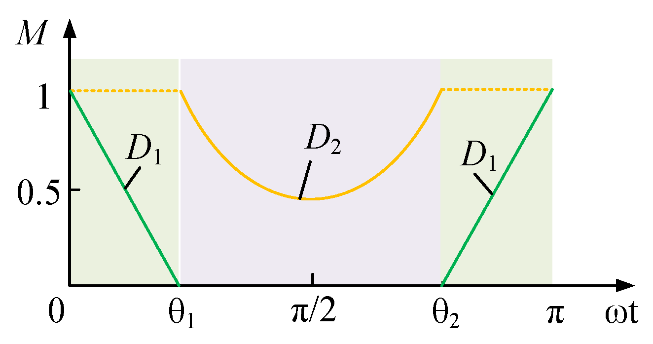
3.2. Modulation Strategy

In this paper, the multi-carrier PWM modulation strategy is used to generate a switching pulse distribution for the proposed PDBCs. The PDBC-II is used as an example to illustrate the switching pulse distribution and bridge arm voltages uaN, ubN of the multi-carrier PWM modulation strategy, as shown in Figure 8, where vc1(t), vc2(t), vc3(t), vc4(t) and vref(t) represent four carrier signals and the reference signal, respectively. The reference signal, vref(t), is compared to vc1(t), vc2(t), vc3(t) and vc4(t) to obtain the switching pulse waveform of the switches S1, S2, S3 and S4, respectively.
In the positive half-cycle of the PWM modulation strategy, the duty cycle can be derived from Equations (2)–(6), below. For these Equations, Ug,max, Ton and Toff are the amplitude of AC voltage and the turn on and off times of the switch, respectively. The modulation ratio M and duty ratio D can be defined as follows:
M = U g , max / U dc
and
D = T on / ( T on + T off ) .
When 0 < vref(t) < 0.5, the PDBCs operate alternately in Working modes 1 and 2. At this time, the inductance volt-second balance has the following relationship:
( u g 0.5 U dc ) T on = ( U dc u g ) T off .
The duty cycle D1 is derived from Equations (2)–(4):
D 1 = 1 2 M sin ( w t ) .
Similarly, when 0.5 < vref(t) < 1, the PDBCs operate alternately in Working modes 2 and 3. The duty cycle D2 can be obtained as follows:
D 2 = 2 2 M sin ( w t ) .
When the PDBCs operate in the positive half-cycle, the resulting duty cycle change curve, based on Equations (5) and (6), is shown in Figure 9,where the green curve represents the duty cycle D1, the yellow curve represents the duty cycle D2 and θ1 and θ2 are the angles of alternation between vc1(t) and vc2(t), respectively.
It is assumed that, the amplitude of vref(t) is 1 (after normalization) and the θ1 and θ2 can be calculated as follows:
θ 1 = arcsin 0.5 = π 6
D 2 = 2 2 M sin ( w t ) .

4. Performance Analysis

4.1. Voltage Stress Analysis

Based on the working mode analysis of Figure 6, the switch and diode voltage stresses of the three PDBCs are summarized, as shown in Table 2. It can be seen from Table 2 that part of the components voltage stress on the three-level bridge is reduced by half. In addition, the PDBC-II and PDBC-III have three components with voltage stresses of reduced by half, while the PDBC-I has only two components with voltage stresses reduced by half. Therefore, in terms of cost, PDBC-II and PDBC-III have lower costs compared to PDBC-I.

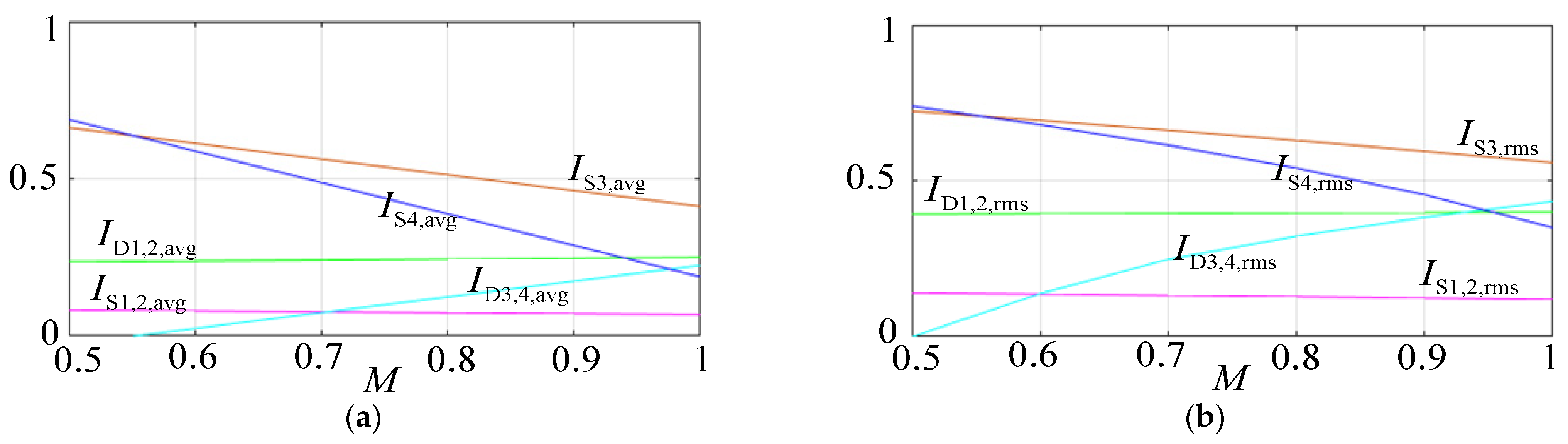
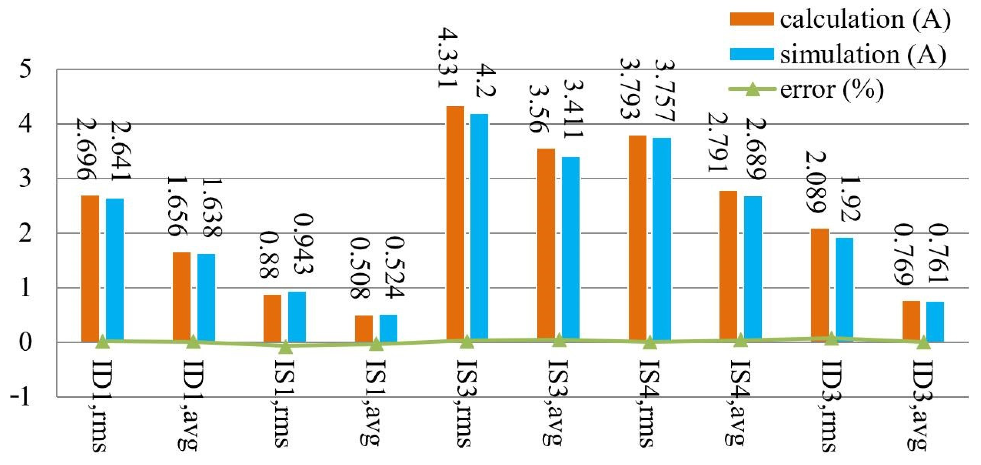
4.2. Current Stress Analysis

To estimate the conduction loss of the switches and diodes, it is necessary to calculate the average and the root mean square (RMS) of the current flowing through the switches and diodes. In this section, the PDBC-II is used as the example in which the current stress analysis is conducted. Figure 10 shows the current stress simulation waveform of PDBC-II in the Matlab/Simulink environment. It is clear, from Figure 9 and Figure 10, that the switching times of the duty cycles D1 and D2 are Tg/12 and 5Tg/12 (Tg is one power frequency cycle), respectively. Based on Figure 10, the theoretical derivation of the average value and RMS value of the current flowing through the semiconductor device can be calculated using Equation (9) through (18). For the following calculations, it is assumed that the AC side current is a sine wave, the DC side voltage remains unchanged, and the switching frequency fs is much greater than the grid frequency fg.
The current RMS and average of the diodes D1 and D2 are calculated using Equation (9):
{ I D 1 , 2 , rms 2 = 2 T g [ 0 T g 12 ( 1 D 1 ) i g 2 d t + T g 12 T g 4 ( i g + 0 . 5 I g , max 2 ) 2 d t ] I D 1 , 2 , avg = 2 T g [ 0 T g 12 ( 1 D 1 ) i g d t + T g 12 T g 4 ( i g + 0 . 5 I g , max 2 ) d t ] .
Substituting Equation (5) into Equation (9), the current RMS and average of diodes D1 and D2 can be obtained:
{ I D 1 , 2 , rms = 6 I g , max 24 π 6 π + 15 3 + ( 128 72 3 ) M I D 1 , 2 , avg = I g , max 12 π [ π + 3 3 + ( 2 π 3 3 ) M ] .
The current RMS and average of the MOSFET S1 and S2 are calculated using Equation (11):
{ I S 1 , 2 , rms 2 = 2 T g [ 0 T g 12 D 1 i g 2 d t + 7 T g 12 3 T g 4 ( i g + 0.5 I g , max 2 ) 2 d t ] I S 1 , 2 , a v g = 2 T g [ 0 T g 12 D 1 i g d t + 7 T g 12 3 T g 4 | i g + I g , max 2 | d t ] .
Substituting Equation (5) into Equation (11), the current RMS and average of the MOSFET S1 and S2 can be obtained:
{ I S 1 , 2 , rms = 6 I g , max 24 π 14 π 21 3 + ( 72 3 128 ) M I S 1 , 2 avg = I g , max 12 π [ 12 π 3 3 + ( 3 3 2 π ) M ] .
The current RMS and average of MOSFET S3 is calculated using Equation (13):
{ I S 3 , rms 2 = 4 T g [ 0 T g 12 D 1 i g 2 d t + T g 12 T g 4 D 2 i g 2 d t + T g 2 3 T g 4 i g 2 d t ] I S 3 , avg = 2 T g [ 0 T g 12 D 1 i g d t + T g 12 T g 4 D 2 i g d t + T g 2 3 T g 4 | i g | d t ] .
Substituting Equations (5) and (6) into Equation (13), the current RMS and average of MOSFET S3 can be obtained:
{ I S 3 , rms = I g , max 2 3 π 3 3 + 10 π 32 M I S 3 , avg = I g , max π ( 3 + 2 π M ) .
The current RMS and average of MOSFET S4 is calculated using Equation (15):
{ I S 4 , rms 2 = 4 T g [ 0 T g 12 D 1 i g 2 d t + T g 12 T g 4 D 2 i g 2 d t ] I S 4 , avg = 4 T g [ 0 T g 12 D 1 i g d t + T g 12 T g 4 D 2 i g d t ] .
Substituting Equations (5) and (6) into Equation (15), the current RMS and average of MOSFET S4 can be obtained:
{ I S 4 , rms = I g , max 2 3 π 3 3 + 10 π 32 M I S 4 , avg = I g , max π ( 3 + 2 π M ) .
The current RMS and average of diodes D3 and D4 current is calculated using Equation (17):
{ I D 3 , 4 , rms 2 = 2 T g [ 0 T g 12 ( 1 D 1 ) i g 2 d t + T g 12 T g 4 ( 1 D 2 ) i g 2 d t ] I D 3 , 4 , avg = 4 T g [ 0 T g 12 ( 1 D 1 ) i g d t + T g 12 T g 4 ( 1 D 2 ) i g d t ] .
Substituting Equations (5) and (6) into Equation (17), the current RMS and average of diodes D3 and D4 can be obtained:
{ I D 3 , 4 , rms = I g , max 2 6 π 32 M 3 3 4 π I D 3 , 4 , avg = I g , max 2 π ( π M 3 ) .
Figure 11 shows the change curve of the current average and RMS of the switches and diodes with the modulation ratio, M, after normalization of Ig,max. It can be seen from Figure 11 that the current RMS value and average for each of the components have the same trend. Since Ig,max are normalized, the trend shown in Figure 11 is also applicable under different power levels, which is of great significance for studying the working principle of the rectifier.
To verify the correctness of the current stress formula developed in this paper, the current stress value of the switches and diodes is measured in the Matlab/Simulink environment under a 1 kW power rate. Figure 12 shows the comparison between the calculated value and the simulated value of the current stress. It can be seen from Figure 12, the calculated current stress in this paper is consistent with the simulated value, which verifies the correctness of the current stress formula.

4.3. Loss Analysis

Based on the above current stress analysis, this section analyzes the loss and efficiency of the proposed PDBCs. The losses of the MOSFET mainly include conduction losses and switching losses. When the MOSFET is on-state, the on-state resistance, rds, results in the conduction losses. The conduction losses Pcon can be calculated as (19), where IS,rms is the RMS value of the current flowing through the MOSFET, which can be obtained from the current stress analysis:
P con = I S , rms 2 r ds .
During the drain current and voltage conversion processes of the MOSFET, the switching losses are generated. These can be calculated using Equation (20), where Uin, Io, ton, toff, and fs are the RMS value of the input voltage, the output current, the switching process drain current and voltage conversion crossover time and the switching frequency, respectively:
P sw = 0.5 U in I o ( t on + t o f f ) f s .
Similarly, the power losses of the diode in a cycle consists mainly of static losses and dynamic losses. For the static losses, since the fast recovery diode is employed in this paper, there are only on-state losses considered. The dynamic losses of the diode can be calculated with Equation (21), where Uf is the forward conduction voltage, ID,avg is the average value of the diode:
P Son = 0 T g u i d t / T g = U f I D , avg .
Compared to the reverse recovery time, tr, the forward recovery time, tf, is negligible; therefore, the turn-on losses can be ignored. The turn-off losses can be calculated using Equation (22), where Urp and Irp are the reverse peak voltage and current, tb is the reverse current fall time:
P Doff = t 0 t 2 u F ( t ) i F ( t ) d t / T S = 0.5 U rp I rp t b f s
In this paper, the MOSFETs and diodes employ IRFP450 and RHRP3060, respectively. According to the data sheets, the parameters for IRFP450 and RHRP3060 are shown in Table 3. The switching frequency is fs = 20 kHz.
Based on Equation (9) through (22), the losses of the proposed three PDBCs and the CFLC at different output powers are calculated. According to the results of the loss calculations, the efficiency diagrams at different output power rates are generated, as shown in Figure 13. From this, it can be seen that the four circuits reach peak efficiency at approximately 300 W. However, when the output power is over 300 W, the efficiency declines slowly as the output power increases. The peak efficiency of the PDBC-I is 98.27%, which is the highest in the four circuits. In addition, as the output power level increases, the efficiency of the PDBC-I reaches the highest of the four circuits. Therefore, the PDBC-I is more suitable at a higher power rate. Figure 13b shows the experimental efficiency and theoretical efficiency of the PDBC-II circuit, and the efficiency analysis is expressed in the Figure 13b. The maximum experimental efficiency is approx. 96.5%, which is lower than the theoretical efficiency. Since there are actual circuits that exist as auxiliary circuits (drive circuit, sampling circuit, et al.), the actual loss is higher than those in the theoretical analysis results. Nevertheless, in the theoretical calculation and practical experimental results, the trend of overall efficiency distribution is consistent.

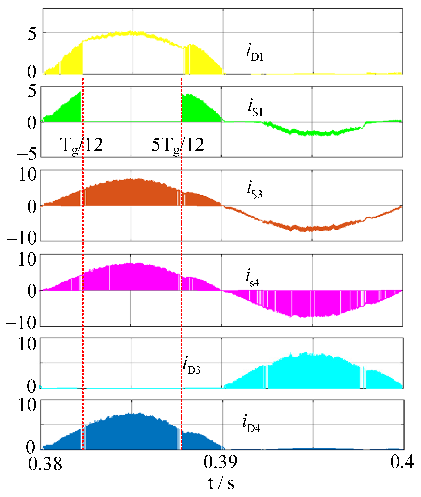
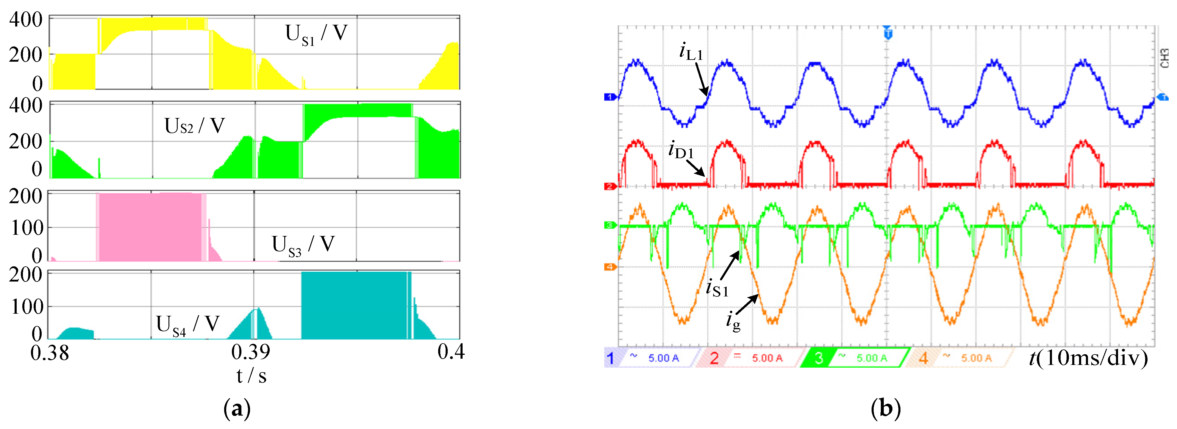
5. Experimental Verification

In order to verify the feasibility of the PDBC proposed in this paper and the correctness of the theoretical analysis, PDBC-II [shown in Figure 4b] is selected for corresponding experimental verification, as shown in Figure 14. The experimental circuit design includes an EMI circuit, auxiliary power supply, main power circuit, signal sampling circuit, MOSFET drive circuit and protection control circuit. The controller employs DSP28335 and the MOSFETs and diodes employ IRFP450 and RHRP3060, respectively; the experimental circuit parameters are shown in Table 4.
Figure 15 shows the PDBC-II steady-state experimental waveforms of the input and output sides at 1 kW rated power. Figure 15a shows the voltage waveforms of the single-phase AC power supply voltage, ug, the input side current, ig, the DC side voltage, Udc, and UC1 and UC2. As seen from Figure 15a, the input power supply voltage, ug, is in phase with the input side current, ig, and it is sufficiently consistent to achieve power factor correction. The DC side voltage, Udc, is stable at 400 V, and the capacitor voltages UC1 and UC2 remain dynamically balanced at 200 V. Figure 15b shows the bridge arm voltage uaN, ubN waveform and the input inductor current iL1, iL2 waveform. As can be seen from Figure 15b, the waveform of inductor current iL1 phase is ahead 180° of the inductor current iL2. Similarly, the bridge arm voltage uaN, ubN waveform changes in positive and negative half-cycles alternately, which is consistent with Figure 6 and Table 1.
Figure 16 shows the PDBC-II switching pulse distribution experimental waveform. As can be seen from Figure 16, the switches S1–S4 have a short, high-frequency switching time. As a result, the switching losses of PDBC-II are relatively low. In addition, the switches S3 and S4 symmetrically action in positive and negative half-cycles, which is consistent with the switching pulse distribution of Table 1.
Figure 17 shows the PDBC-II voltage and current stress experimental waveforms of the switches at 1 kW rated power. Figure 17a shows the voltage stress waveforms of the switches S1–S4. It can be seen from Figure 17a that the maximum voltage stress of the four switches is US1 = US2 ≈ 400 V and US3 = US4 ≈ 200 V; i.e., the partial voltage stress is halved, which is consistent with the voltage stress analysis in Table 2. Figure 17b shows the waveform of the inductor current, diode D1 current, iD1 and the switch S1 current, iS1. As can be seen here, the waveform of the switch current iS1 is enveloped by the waveform of the current iL1 of the inductor L1 in the positive half cycle. In addition, the currents iD1 and iS1 change at high frequencies during the [0, Tg/12] and [5Tg/12, Tg/2] (where Tg is the grid period), which is the same as the simulation waveforms in Figure 10.
Figure 18 shows the THD test results of PDBC-II at 1 kW rated power. As can be seen here, at the switching frequency of 20 kHz, the THD of PDBC-II is 3.2%, which meets the IEC 6100-3-2 standard.

6. Conclusions

In this paper, combining the three-level PTP circuit and the five-level NPC bridge arm, a family of PDBCs is proposed by transforming the NPC bridge arm. The proposed circuit reduces the volume of the filter inductor to increase the power density of the circuit and improves the working efficiency of the circuit. Through comparative analyses of voltage and current stress and loss, the following conclusions are drawn.
(1)
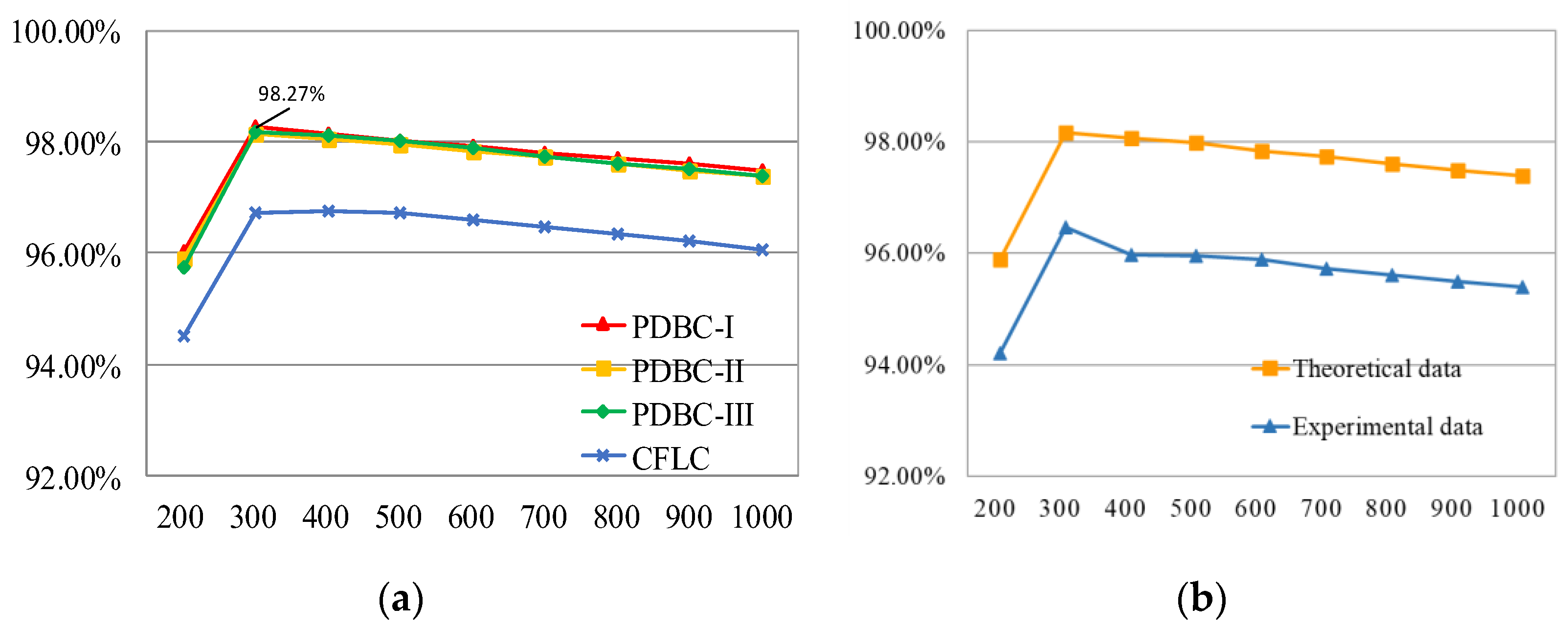
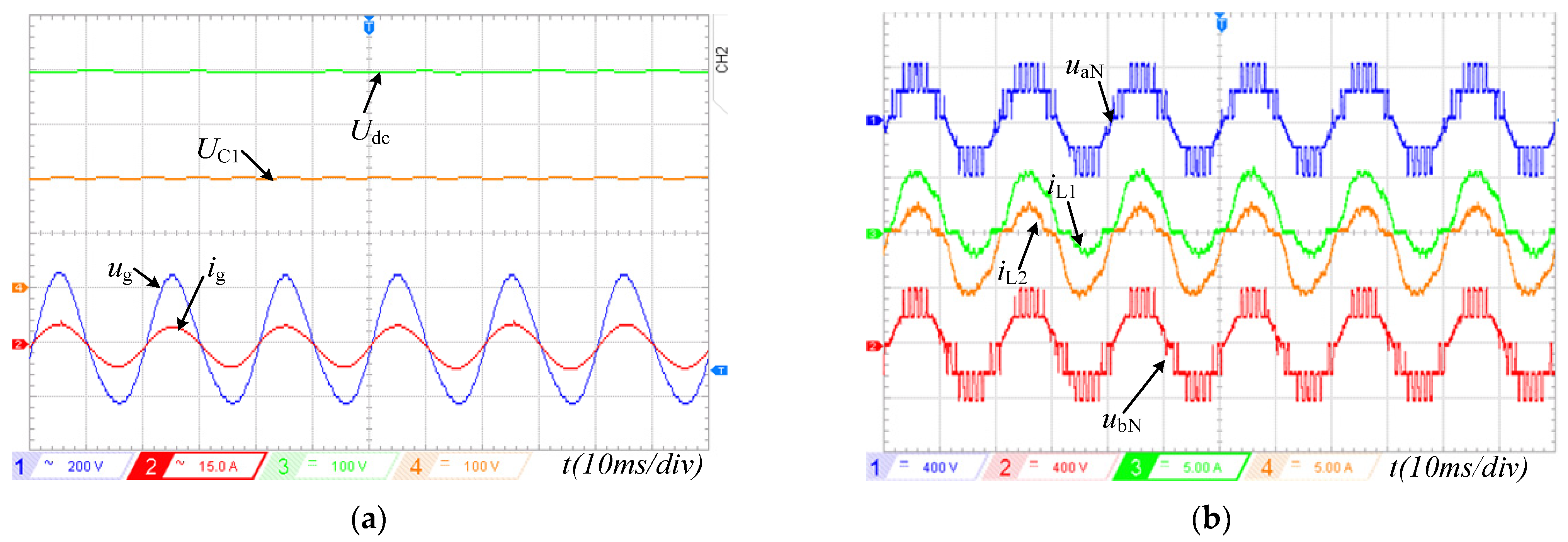
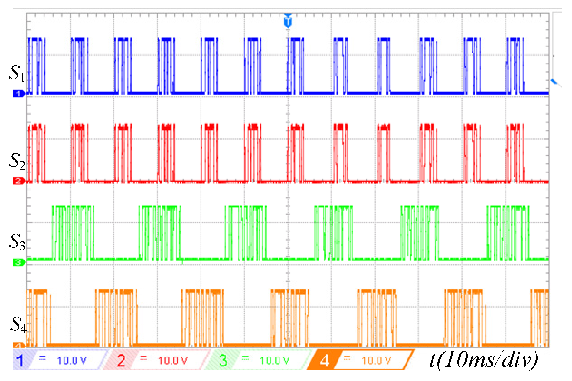
The experimental results show that the PDBCs proposed in this paper have good input and output waveforms at low switching frequency. Therefore, the PDBCs can improve overall efficiency by reducing switching losses.
(2)
The efficiency of the five PDBCs proposed in this paper is higher than that of a CFLC. The PDBC-I has the smallest loss and the highest efficiency, with a peak efficiency of 98.27%, and its overall performance is the best.
(3)
Compared with the conventional three-level PTP circuit, the five PDBCs proposed in this paper have higher power density, and the voltage stress of some devices is reduced by half. In addition, the PDBC-II and PDBC-III have more devices with voltage stresses halved; thus, their cost is lower.

Author Contributions

Conceptualization, C.J.; Methodology, G.M.; Validation, Q.Z.; Resources, W.L.; Data curation, H.D.; Writing—original draft, Q.Z.; Writing—review & editing, J.X.; Supervision, H.M. All authors have read and agreed to the published version of the manuscript.

Funding

This research was funded by the Hubei Provincial Key Laboratory for Operation and Control of Cascaded Hydropower Station (China Three Gorges University), China grant number [2022KJX05].

Data Availability Statement

Not applicable.

Conflicts of Interest

The authors declare no conflict of interest.

References

  1. Shah, M.T.; Chauhan, S.K.; Tekwani, P.N. Analysis of multiaxis current controller for power system friendly front-end converter employing two-level and three-level topologies. IEEE Trans. Ind. Electron. 2021, 68, 586–597. [Google Scholar] [CrossRef]
  2. Li, K.; Formentini, A.; Dewar, D.; Zanchetta, P. Controller design of an active front-end converter keeping in consideration grid dynamic interaction. IEEE Trans. Ind. Electron. 2022, 69, 5195–5206. [Google Scholar] [CrossRef]
  3. Gendrin, M.; Gauthier, J.; Lin-Shi, X. A predictive hybrid pulse-width-modulation technique for active-front-end rectifiers. IEEE Trans. Power Electron. 2017, 32, 5487–5496. [Google Scholar] [CrossRef]
  4. Kang, C.; Wang, W.; Li, W.; Du, H.; Diao, L. Balance midpoint potential control of three-level boost converter for rail transit application. IEEE Access 2019, 7, 47737–47746. [Google Scholar] [CrossRef]
  5. Ebrahimi, J.; Karshenas, H.; Bakhshai, A. A five-level nested diode-clamped converter for medium-voltage applications. IEEE Trans. Ind. Electron. 2022, 69, 6471–6483. [Google Scholar] [CrossRef]
  6. Zhang, Y.; Bai, Y.; Yang, H.; Zhang, B. Low switching frequency model predictive control of three-level inverter-fed IM drives with speed-sensorless and field-weakening operations. IEEE Trans. Ind. Electron. 2019, 66, 4262–4272. [Google Scholar] [CrossRef]
  7. Zhang, G.; Peng, S.; Geng, Q.; Shi, T.; Xia, C. Hybrid discontinuous space vector PWM strategy for three-level inverters under two-phase loads condition. IEEE Trans. Power Electron. 2022, 37, 1711–1721. [Google Scholar] [CrossRef]
  8. Montero-Robina, P.; Umbría, F.; Salas, F.; Gordillo, F. Integrated control of five-level diode-clamped rectifiers. IEEE Trans. Ind. Electron. 2019, 66, 6628–6636. [Google Scholar] [CrossRef]
  9. Sebaaly, F.; Vahedi, H.; Kanaan, H.Y.; Al-Haddad, K. Experimental design of fixed switching frequency model predictive control for sensorless five-level packed U-cell inverter. IEEE Trans. Ind. Electron. 2019, 66, 3427–3434. [Google Scholar] [CrossRef]
  10. Siwakoti, Y.P.; Palanisamy, A.; Mahajan, A.; Liese, S.; Long, T.; Blaabjerg, F. Analysis and design of a novel six-switch five-level active boost neutral point clamped inverter. IEEE Trans. Ind. Electron. 2020, 67, 10485–10496. [Google Scholar] [CrossRef]
  11. He, L.; Cheng, C. A flying-capacitor-clamped five-level inverter based on bridge modular switched-capacitor topology. IEEE Trans. Ind. Electron. 2016, 63, 7814–7822. [Google Scholar] [CrossRef]
  12. Gautam, S.P.; Kumar, L.; Gupta, S.; Agrawal, N. A single-phase five-level inverter topology with switch fault-tolerance capabilities. IEEE Trans. Ind. Electron. 2017, 64, 2004–2014. [Google Scholar] [CrossRef]
  13. Alsofyani, I.M.; Lee, K.-B. Simple capacitor voltage balancing for three-level NPC inverter using discontinuous PWM method with hysteresis neutral-point error band. IEEE Trans. Power Electron. 2021, 36, 12490–12503. [Google Scholar] [CrossRef]
  14. Zhang, Y.; Li, C.; Li, C.; Xin, Z.; Chen, R.; Li, W.; He, X.; Ma, H. A SiC and Si hybrid five-level unidirectional rectifier for medium voltage applications. IEEE Trans. Ind. Electron. 2022, 69, 7537–7548. [Google Scholar] [CrossRef]
  15. Chen, W.; Bazzi, A.M. Model-based voltage quality analysis and optimization in post-fault Reconfigured N-level NPC inverter. IEEE Trans. Power Electron. 2021, 36, 13706–13715. [Google Scholar] [CrossRef]
  16. He, Z.; Ding, H.; Chen, Z.; Zhao, Q.; Xun, Z.; Zhang, D.; Shao, J. A hybrid DPWM for vienna rectifiers based on the three-level to two-level conversion. IEEE Trans. Ind. Electron. 2022, 69, 9429–9439. [Google Scholar] [CrossRef]
  17. Wang, S.; Ma, J.; Liu, B.; Jiao, N.; Liu, T.; Wang, Y. Unified SVPWM algorithm and optimization for single-phase three-level NPC converters. IEEE Trans. Power Electron. 2020, 35, 7702–7712. [Google Scholar] [CrossRef]
  18. Ma, J.; Song, W.; Wang, S.; Feng, X. Model predictive direct power control for single phase three-level rectifier at low switching frequency. IEEE Trans. Power Electron. 2018, 33, 1050–1062. [Google Scholar] [CrossRef]
  19. Kim, J.; Lee, S.; Cha, W.; Kwon, B. High-efficiency bridgeless three-level power factor correction rectifier. IEEE Trans. Ind. Electron. 2017, 64, 1130–1136. [Google Scholar] [CrossRef]
  20. Liu, Z.; Xia, Z.; Li, F.; Wang, G.; Li, C. A capacitor voltage precharge method for back-to-back five-level active neutral-point-clamped converter. IEEE Trans. Ind. Electron. 2021, 68, 9277–9286. [Google Scholar] [CrossRef]
  21. Zhang, L.; Sun, K.; Xing, Y.; Zhao, J. A family of five-level dual-buck full-bridge inverters for grid-tied applications. IEEE Trans. Power Electron. 2016, 31, 7029–7042. [Google Scholar] [CrossRef]
  22. Rech, C.; Castiblanco, W.A.P. Five-level switched-capacitor ANPC inverter with output voltage boosting capability. IEEE Trans. Ind. Electron. 2022, 70, 29–38. [Google Scholar] [CrossRef]
  23. Monteiro, V.; Ferreira, J.C.; Meléndez, A.A.N.; Afonso, J.L. Model predictive control applied to an improved five-level bidirectional converter. IEEE Trans. Ind. Electron. 2016, 63, 5879–5890. [Google Scholar] [CrossRef]
  24. Ma, H.; Zheng, K.; Jiang, H.; Yin, H. A family of dual-boost bridgeless five-level rectifiers with common-core inductors. IEEE Trans. Power Electron. 2021, 36, 12565–12578. [Google Scholar] [CrossRef]
  25. Vahedi, H.; Shojaei, A.A.; Chandra, A.; Al-Haddad, K. Five-level reduced-switch-count boost PFC rectifier with multicarrier PWM. IEEE Trans. Ind. Appl. 2016, 52, 4201–4207. [Google Scholar] [CrossRef]
Figure 1. The common five-level converter topologies. (a) Conventional five-level converter; (b) Converter proposed in [25].
Electronics 12 03722 g001
Figure 2. Three most commonly used clamping bridge arm structures. (a) T-type three-level bridge arm structure; (b) Diode Neutral Point Clamping (DNPC) three-level bridge arm structure; (c) Single switch three-level bridge arm structure.
Electronics 12 03722 g002
Figure 3. Topology derivation. (a) Topology derivation of A2; (b) Topology derivation of A3.
Electronics 12 03722 g003
Figure 4. A family of five-level PTP dual boost converters. (a) PDBC-I; (b) PDBC-II; (c) PDBC-III.
Electronics 12 03722 g004
Figure 5. Key waveforms of six working modes in one cycle.
Electronics 12 03722 g005
Figure 6. The six working mode of PDBC-II. (a) Working mode 1; (b) Working mode 2; (c) Working mode 3; (d) Working mode 4; (e) Working mode 5; (f) Working mode 6.
Electronics 12 03722 g006
Figure 7. Control block diagram of the PDBCs.
Electronics 12 03722 g007
Figure 8. Diagram of modulation strategy.
Electronics 12 03722 g008
Figure 9. Change curve of duty cycle in the positive half-cycle.
Electronics 12 03722 g009
Figure 10. The current stress of PDBC-II.
Electronics 12 03722 g010
Figure 11. Power component average & RMS current stress as functions of the modulation ratio M normalized: Ig,max. (a) Average value; (b) RMS value.
Electronics 12 03722 g011
Figure 12. Current stress comparison of calculated and simulated value.
Electronics 12 03722 g012
Figure 13. Diagram of efficiency analysis. (a) Efficiency analysis of the theoretical calculation; (b) Experimental efficiency analysis of the PDBC-II.
Electronics 12 03722 g013
Figure 14. Experimental platforms.
Electronics 12 03722 g014
Figure 15. Steady-state experimental waveforms. (a) The voltage waveforms of power supply voltage ug, current ig, and the DC side voltage Udc, UC1, UC2; (b) The bridge arm voltage uaN, ubN and the inductor current iL1, iL2.
Electronics 12 03722 g015
Figure 16. Switching pulse distribution experimental waveform.
Electronics 12 03722 g016
Figure 17. Voltage and current stress experimental waveforms. (a) The voltage stress waveform of switches S1–S4; (b) The inductor current iL1, diode D1 current iD1, and the switch S1 current iS1.
Electronics 12 03722 g017
Figure 18. THD test results of PDBC-II.
Electronics 12 03722 g018
Table 1. Switching pulse distribution of PDBC-II.
ModeigS1S2S3S4C1C2uaNubN
1>010000ug
2>00010Udc/2Udc/2
3>00000UdcUdc
4<00100ug0
5<00001−Udc/2−Udc/2
6<00000−Udc−Udc
Table 2. Voltage stress of three PDBCs.
ComponentsPDBC-IPDBC-IIPDBC-III
S1,2UdcUdcUdc
S3,4Udc/2Udc/2Udc/2
D1,2UdcUdcUdc
D3UdcUdc/2Udc
D4UdcUdcUdc/2
Table 3. Component parameters.
ComponentsParametersValues
IRFP450On-state resistance, rds0.4 Ω
On-delay time, td(on)17 ns
Rise time, tr47 ns
Turn-off delay time, td(off)92 ns
Fall time, tf44 ns
RHRP3060Conduction voltage, Uf1.7 V
Reverse peak voltage, Urp600 V
Reverse peak current, Irp250 μA
Reverse current fall time, tb18 ns
Table 4. Main parameters.
ParametersLabelValue
Input filter inductorsL1, L22 mH
DC-side capacitorsC1, C21000 μF
Input voltageugRMS 220 V
Output voltageUdc400 V
Rated output powerPo1000 W
Grid frequencyfg50 Hz
Switching frequencyfs20 kHz
Disclaimer/Publisher’s Note: The statements, opinions and data contained in all publications are solely those of the individual author(s) and contributor(s) and not of MDPI and/or the editor(s). MDPI and/or the editor(s) disclaim responsibility for any injury to people or property resulting from any ideas, methods, instructions or products referred to in the content.

