Article

FPGA-Based Optimization of Industrial Numerical Machine Tool Servo Drives

Department of Intelligent Computer Systems, Czestochowa University of Technology, 42-201 Częstochowa, Poland
Electronics 2023, 12(17), 3585; https://doi.org/10.3390/electronics12173585
Submission received: 13 July 2023 / Revised: 14 August 2023 / Accepted: 22 August 2023 / Published: 24 August 2023
(This article belongs to the Special Issue Design and Development of Digital Embedded Systems)

Abstract

:
This paper presents an analysis of the advantages stemming from the application of field-programmable gate arrays (FPGAs) in servo drives used within the control systems of industrial numerical machine tools. The method of improving the control system that allows for increasing the precision of machining, as well as incorporating new functionalities and streamlining diagnostic processes, is described. As demonstrated, the utilization of digital controllers with robust computational power and high-performance real-time communication interfaces is essential for achieving these objectives. This study underscores the limitations of commonly employed digital controllers in servo drives, which are constructed based on microcontrollers or signal processors collaborating with application-specific integrated circuits (ASICs). In contrast, the proposed FPGA-based solution offers substantial computational power and significantly reduced latencies in the real-time communication interface compared to other examined alternatives. This enables the realization of the planned objectives, specifically the enhancement of technical parameters and diagnostic capabilities of machine tools. Furthermore, the research indicates that FPGA-based digital controllers exhibit relatively low power consumption and a simplified design of the electronic printed circuit board in comparison to other analyzed digital platforms. These features can contribute to heightened reliability and diminished production costs of such controllers. Additional conclusions drawn from the study indicate that FPGA-based controllers provide greater developmental possibilities and their production is marked by potential resilience to challenges associated with the availability of electronic components in the market.

1. Introduction

The significant progress that has been made in recent decades in the area of industrial numerical machine tools results from many factors. First of all, the newly developed technologies for high-speed milling (HSM), high-pressure water jet cutting, or cutting with high-power semiconductor laser light delivered via optical fiber should be mentioned here. Examples of such machines are shown in Figure 1. Improvements to machines in terms of increasing the speed and precision of their work also result from the use of more and more perfect mechanical structures, drive motors with better parameters, more precise sensors, and more perfect electronic and power electronic components. Obtaining high-quality work with industrial machine tools would of course not be possible without a control system with adequate parameters.
The control system that meets the high requirements of modern machine tools is based on complex algorithms implemented in its controllers. These algorithms take into account some phenomena in the field of material processing technology (milling, cutting with a water jet, or fiber laser beam) and motion dynamics. Controllers on which such algorithms are implemented must have sufficiently high computing power and at the same time the ability to work in real time. Such controllers must therefore provide a deterministic response time to the required measurement and reference signals. In other words, they should generate signals that control the actuators and, through them, the machining process quickly enough. In addition, they must be able to work in the harsh industrial conditions that usually prevail in factories, i.e., to work in the presence of electromagnetic interference, vibrations, high temperature, high dust, or moisture. This often requires placing such controllers in hermetic housings, which makes it difficult to dissipate the heat that is a side effect of their work. Therefore, it is advisable to reduce heat losses arising in their components. These losses are proportional to the amount of electricity used.
An important factor influencing the assessment of the machine tool as a whole are also other parameters of the control system, such as dimensions, purchase cost, time of failure-free operation, and the cost of work resulting, among other things, from the amount of electricity consumed.
The second section of the paper presents the specifics of control systems for industrial machine tools. The third section describes experimental research along with a detailed analysis of the results, while the fourth section presents the conclusions.

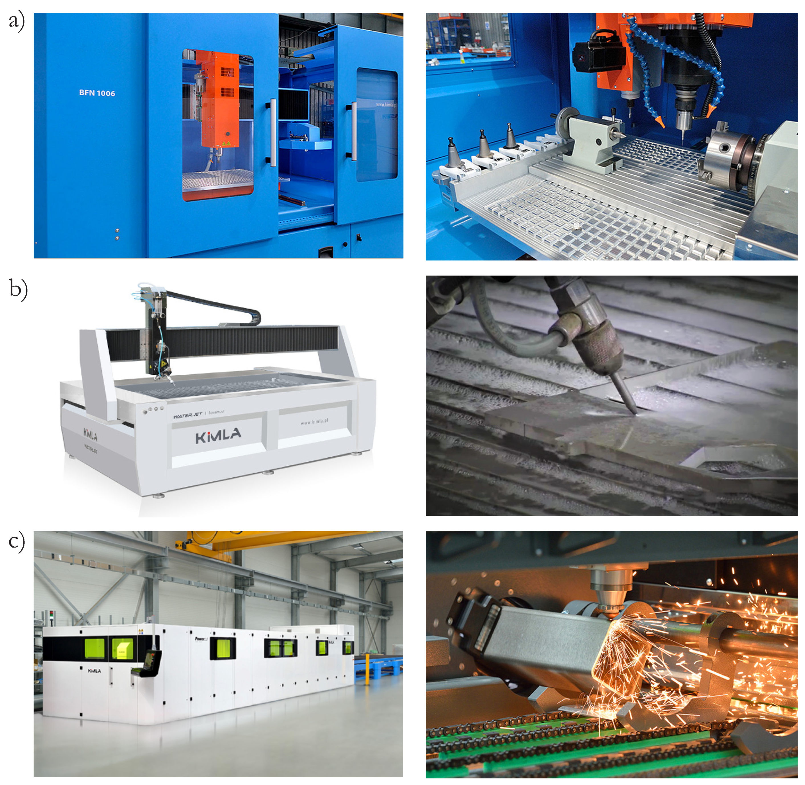
2. Specificity of Control Systems for Industrial Machine Tools

To obtain high reliability, scalability, serviceability, and an acceptable cost of production of a complex control system for industrial machine tools, modern digital solutions based on a modular structure are usually used. In such a construction, the controllers of individual elements of the machine tool are made as separate devices communicating with each other via an appropriately efficient real-time communication interface. Currently, the most commonly used interface is real-time Ethernet (RTE) due to its many advantages [1].
Modular construction, in particular, based on distributed architecture and communication medium in the form of real-time Ethernet, has many advantages. First of all, controllers can be placed close to the devices they control, e.g., electric motors. This allows for a significant reduction in the length of specialist signal and control cables. In addition, if one of the devices fails, it can be easily replaced. The modular system is highly scalable because it can easily adapt to the requirements of different machines by combining various types of controllers. Modernization of a machine tool equipped with a modular control system is also facilitated.
The software that manages the operation of distributed system controllers must also meet several stringent requirements. First of all, due to the specificity of the operation of the machine tool, the algorithms implemented in its controllers must work precisely synchronized with the position of the fast-moving parts of the machine. For example, in currently produced [2] laser cutters, the speed of moving elements reaches several meters per second and acceleration reaches several g, while the control precision is at the level of single micrometers.
To ensure the high precision of the machine tool, the algorithms implemented in its controllers must be performed with the highest possible frequency. Let us use the following example to illustrate the level of these requirements. In the most precise high-speed machine tools, the operating frequency of the electric drive control algorithm is usually around 20 kHz [3]. (As a side note, it should be noted that a further increase in the operating frequency of this algorithm is usually not possible, as the parameters of their power electronic actuators, i.e., insulated-gate bipolar transistors (IGBTs), are the limitation.) The above fact shows that the time available for the controller to perform a full cycle of the control process is in the order of several tens of microseconds. At the same time, within this very short time, the controller must successively: acquire data, process them based on an appropriate algorithm, and finally transfer the calculation results to the actuators. All these stages must be completed before starting the next cycle of the control algorithm.
Data acquisition in this case consists in measuring analog and digital signals connected directly to the controller and receiving control data sent to it via real-time Ethernet. The sender of this data is the central controller that controls the movement of the entire machine, called the interpolator (Figure 2).
At this point, the specificity of control systems should be summarized. As mentioned above, a typical control algorithm requires the shortest possible processing time in most cases. This is because this value determines the total system response time, which is a critical parameter in most control systems. In addition, control systems cannot process further inputs until the current control cycle is complete. For this reason, it is not possible to apply pipelining at the level of control signals.

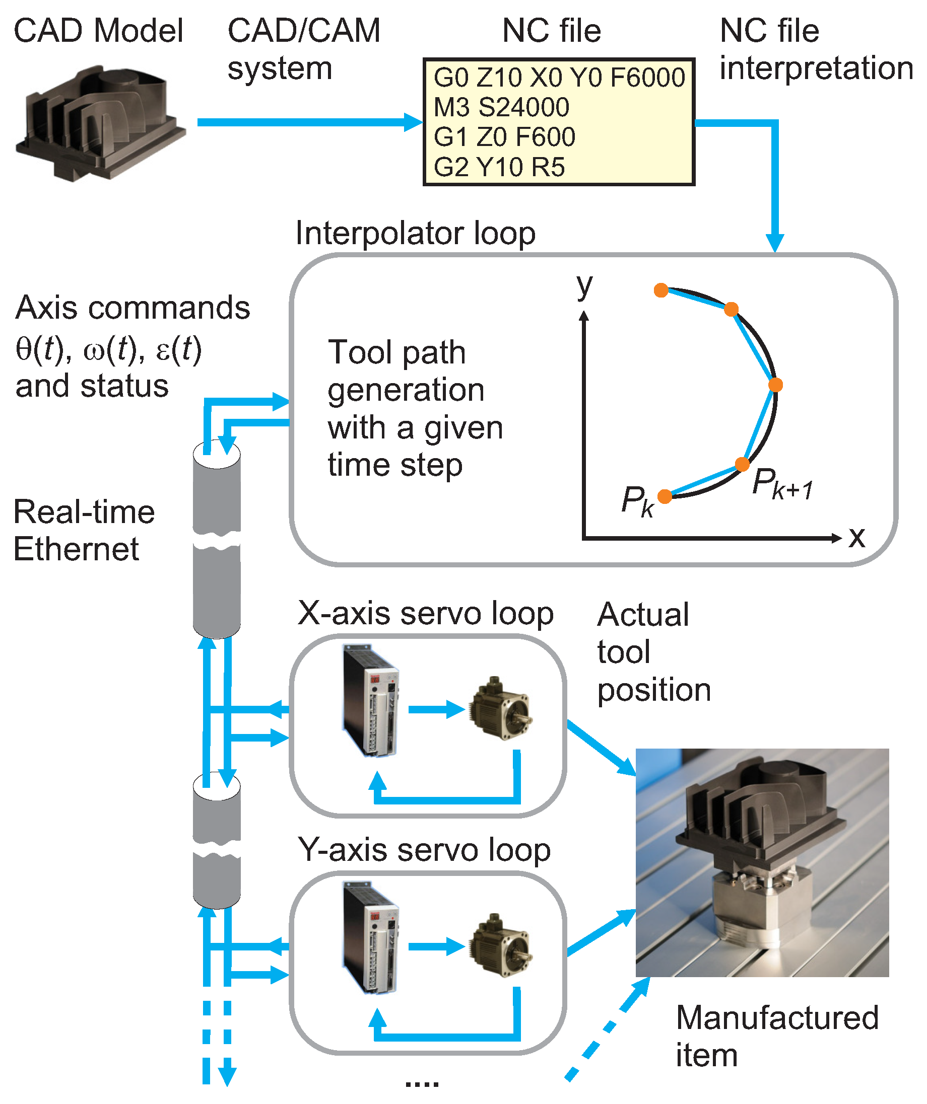
2.1. The Structure of a Distributed Control System

The central controller of the distributed control system (Figure 2), i.e., the interpolator, is primarily responsible for reference trajectory generation and transmitting it via RTE to individual drives of the machine tool and for supervising their operation.
The task of generating a reference trajectory with appropriate parameters is quite a complex process [4]. In addition, as in the case of electric servo drives, this task must be performed in precisely measured and very short interpolation cycles (for example, about 100 ms) to ensure the highest quality of machine tool work. This requirement results from the fact that, in each of these interpolation cycles, successive points of the trajectory are determined. They define set values for the servo drives that control the individual axes of the machine tool. This process is shown in the middle part of Figure 2, where an example path shape is shown as a black semi-circle drawn in the XY coordinate system. Two consecutive points ( P k , P k + 1 ) of the reference trajectory generated by the interpolator are also visible. The greater the time interval between successive interpolation cycles, the curvature of the geometric path describing the movement of the machine tool is reproduced with lower precision.
Of course, the transfer of data between the master controller, i.e., the interpolator, and its subordinate actuators distributed in the machine’s control system must also be carried out in such cycles and must be synchronized with the operation of the interpolator. This is accomplished using a real-time communication interface.

2.2. Real-Time Ethernet

The properties of the communication medium used determine the amount of data that can be sent from the master controller to the slave controllers and in the opposite direction in a deterministic manner in a given time unit. Many of the real-time communication solutions currently available on the market are collectively referred to as real-time Ethernet solutions. These solutions are based on the physical layer compliant with the IEEE802.3 standard, i.e., Fast Ethernet. The theoretical throughput of this medium is 2 × 100 Mbit/s, i.e., 2 × 12.5 MB/s in full-duplex mode. This is a value that more than meets the requirements of numerical control systems for machine tools, in particular, if only the basic functions of such a system are taken into account, i.e., cyclical transmission of reference trajectory parameters for servo drives controlling machine elements in motion. The amount of such data is usually no more than about one hundred bytes in each communication cycle, i.e., about 1 MB per second. Communication interface support for such an amount of data can usually be successfully implemented by software executed on a single-chip microcontroller unit (MCU) or digital signal processor (DSP).
It turns out, however, that in many cases it is necessary to send up to ten times more data than just the basic data describing the reference trajectory of individual machine drives. This additional data may be required to perform advanced machine service functions or to perform a complex control algorithm. It can also be data transmitting the image from the industrial camera supervising the machining process. The total amount of data transmitted by RTE can therefore be as high as ten megabytes every second [1]. At the same time, these data must be transmitted with full-time determinism to be useful in the control system.
The recording and analysis of large amounts of data with a time step of tens of microseconds is extremely useful in the control systems of numerical machine tools. First of all, it significantly improves all service and development work of such a system. However, to achieve this functionality, the controllers must send up to several hundred additional bytes of data in each communication cycle, i.e., several megabytes per second. It should be remembered that this transmission must be performed in a time-deterministic manner. Of course, the transmission of these additional data cannot negatively affect the controller’s performance of its basic functions, i.e., in this case controlling the electric drive motor. Such functionality requires a sufficiently efficient real-time communication medium, for example, RTE. In general, it can be stated that the higher the throughput and the lower the delay of the RTE interface, while maintaining its full-time regime, the better the parameters of the control system that can be obtained.
Typically, the only solution to meet the high real-time communication requirements mentioned earlier is to use hardware-based data processing. One example is the on-the-fly processing mechanism designed by Beckhoff and used in the EtherCAT [5] and Sercos III solutions. The second is the dynamic frame packing mechanism used in the Profinet IRT solution [6]. Various custom solutions are also available, such as E-LINK [1] used by individual manufacturers.
In general, the results of the research presented in the above-mentioned publications lead to the following conclusion. Namely, the hardware processing of the data stream of the RTE interface allows for a significant reduction in delays in real-time communication compared to the implementation of analogous functions by software.
The use of the mechanism of hardware processing of data streams of the real-time communication interface requires the use of one of the four solutions listed below. The first is based on the use of an application-specific integrated circuit (ASIC) that implements the functions of a given RTE solution in hardware. Such a system is connected to a universal central unit (MCU or DSP) necessary to execute the implemented control algorithm. The second solution is to use an MCU or DSP factory equipped with all required hardware modules [7]. The third solution is to use a signal processor with a built-in programmable real-time unit (PRU) that enables quite efficient hardware–software processing of communication interface signals [8]. The last possible solution is to implement the required hardware functions in the programmable logic of the FPGA.
Each solution has its advantages and disadvantages. Namely, the first of the mentioned solutions is characterized by a relatively high degree of complexity of the electronic part. The printed circuit board (PCB) on which many specialized ASICs must be mounted and interconnected is large and complex. This usually results in higher costs and lower reliability compared to devices built in a compact form. In addition, the performance of such a solution may be significantly limited by the limitations of local communication interfaces connecting individual ASICs on the PCB.
The second solution, although the most convenient for the designer and the most efficient, is unfortunately not always possible to use. This is because an integrated circuit is not always available that integrates all the required hardware modules and a central unit (MCU or DSP) with appropriate parameters. In addition, other, non-obvious arguments may also prove against such a solution. Namely, dedicated integrated circuits do not allow any modification of the hardware processing algorithm implemented in them. As it turns out in practice, sometimes the possibility of such a modification is required. The reason may be the need to improve certain system functions or to fix some detected defects. An example of the latter situation can be found in [9], where it is written “US cyber-security researchers have discovered flaws affecting dedicated crypto-authentication chips at the heart of Siemens’ S7-1500 family of industrial controllers, and related products, which could allow attackers to execute malicious code on these devices”. Another sentence is important here, which states that “because the faults are associated with the controller hardware, they cannot be fixed by software updates or patches”.
There is one more reason to use programmable circuits, such as FPGAs, instead of ASICs. As we have seen over the last dozen or so years, there may be long-term shortages in the availability of individual electronic components on the market. The reasons for this may be, for example, natural disasters, pandemics, or wars. The consequences of the lack of availability of components can be very serious. As stated in publication [10] “commodities, materials, software, electronic components, and other replacement components discontinued at short notice or no longer available on the free market for other reasons in Germany cause damage worth billions”. When solutions based on programmable circuits are used, it is usually possible to replace a given integrated circuit with its numerous substitutes, supplied by the same or another manufacturer. This property results primarily from the high universality of FPGAs but also from their long life cycle [11]. As a result, the production of FPGA-based controllers is characterized by potential resilience to challenges related to the availability of electronic components in the market. Moreover, FPGA-based controllers offer greater development possibilities.
The analysis presented above shows that in many respects the most attractive seem to be solutions offering not only adequately high efficiency, but also the highest possible flexibility, compactness, and energy efficiency. Flexibility should be understood as the possibility of any modification of the algorithms implemented in given systems. The greatest possibilities in this area have solutions based on programmable digital circuits of the FPGA type.
Similar conclusions can also be found in other publications. For example, in paper [12], a fiber channel switch based on FPGA is designed and implemented due to its high speed, low latency, and high-performance transmission capacities. As the authors wrote further, its advanced capacity of transmitting and processing big data opens a bright perspective for smart manufacturing. The thesis presented above also seems to be consistent with a slightly more general and increasingly popular approach to design, collectively referred to as software-defined everything (SDx) [13,14]. The methodology is that components that were traditionally implemented in hardware are instead implemented using software in an embedded system, such as an FPGA. Software-defined radio [15] is one example.

3. Experimental Research

In the further part of this manuscript, three solutions built based on the first and last of these methods will be compared. The comparison will concern the results of the implementation of selected control algorithms for numerical machine tools on various digital platforms. The presented results will confirm the above-mentioned thesis regarding the benefits of using FPGA in the control systems of industrial numerical machine tools.

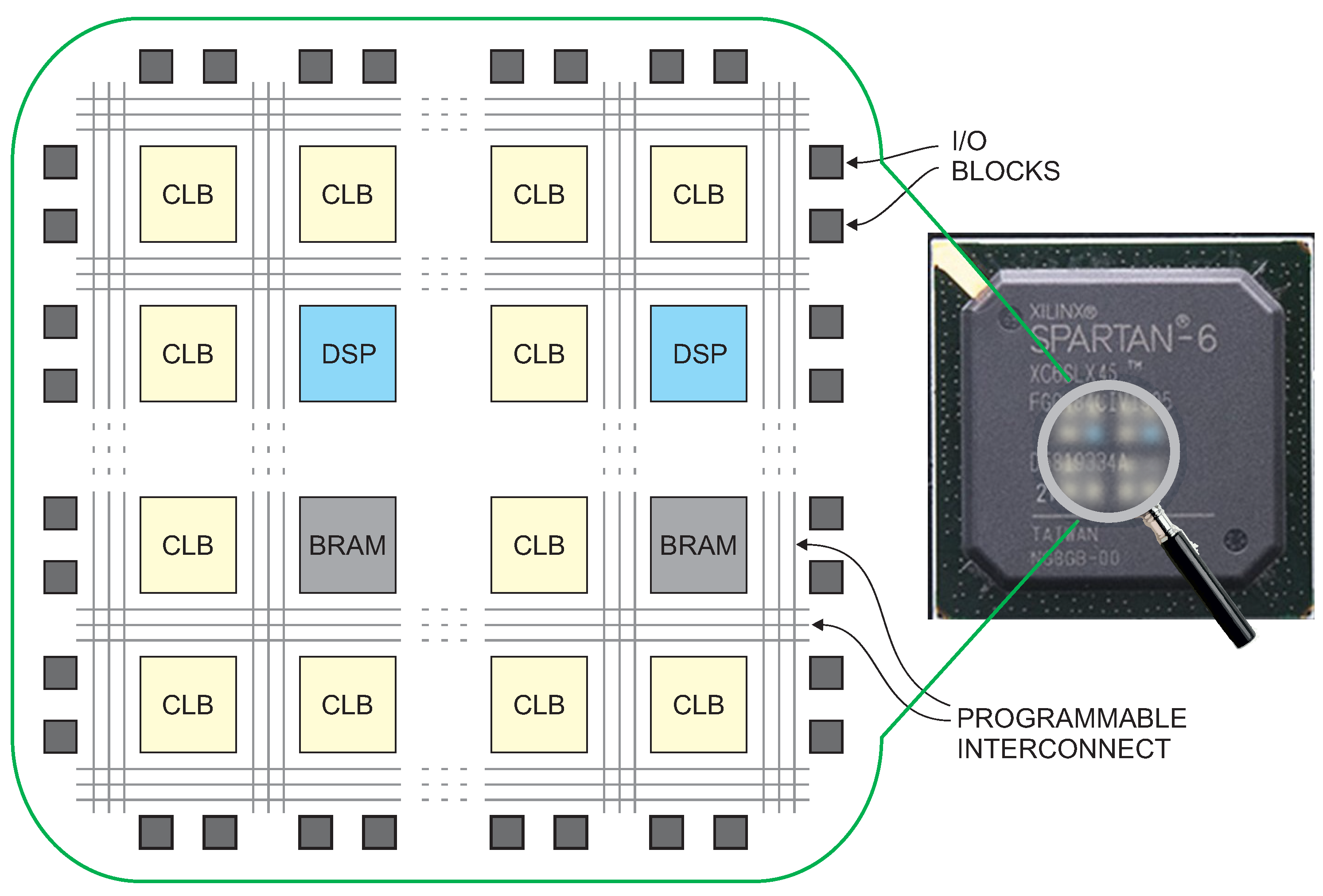
3.1. Architecture and Fundamental Properties of FPGA Devices

A typical FPGA is based on the spatial architecture [16]. Thus, its processing elements such as configurable logic blocks (CLBs) and digital signal processing engines (DSPs) as well as dual-port block RAMs (BRAMs) are arranged in a matrix shape in a silicon structure and are connected by configurable vertical and horizontal lines referred to as programmable interconnects (Figure 3). Such a configurable logic matrix is abbreviated as programmable logic (PL).
In one of the low-end FPGA families available on the market [17] CLB contains logic and look-up tables (LUTs) that can be configured into many different combinations and connected to other components in the PL to create special-purpose functions, processing units, and other entities. Every CLB slice contains four six-input LUTs and eight flip-flops. In addition to the LUTs and flip-flops, the CLB contains arithmetic carry logic and multiplexers to create wider logic functions. The DSP block marked as DSP48A1 consists of, among others, an 18 × 18 two’s-complement multiplier, a 48-bit accumulator, and an adder/subtractor. In turn, each BRAM is a dual-port block RAM, which consists of an 18 Kb memory area and two completely independent access ports. The programmable matrix constructed in this way is surrounded by input–output blocks (I/O blocks), which constitute the PL interface with the FPGA environment.
For clarity, it should be noted that there are also integrated circuits on the market based on FPGA technology, but with heterogeneous architecture, i.e., slightly different from the classical architecture presented in Figure 3. These [18] solutions are referred to as FPGA-system on chip (FPGA-SoC) and are specifically designed to optimize processing performance for dedicated application types. For this purpose, FPGA-SoC solutions include, in addition to the previously described PL part, additional dedicated processing blocks. The FPGA-SoC also includes classic hard-core processors. In particular, the Zynq™ UltraScale+™ FPGA-MPSoC (multi-processor system on chip) family includes several Arm Cortex-A53 64-bit application processors and several Arm Cortex-R5F real-time processors. FPGA-MPSoC devices provide 64-bit processor scalability while combining real-time control with soft and hard engines for graphics, video, waveform, and packet processing. On the other hand, the FPGA-RFSoC family contains, in addition to PL, very fast analog-to-digital (ADC) and digital-to-analog (DAC) converters dedicated to processing radio signals. The area of application of FPGA-RFSoC systems is software-defined radio, including wireless communication and radar systems.
This manuscript applies only to FPGA solutions with classic architecture (Figure 3), including primarily low-end devices. This approach results from the requirements of the considered group of applications. Although low-end FPGAs are characterized by relatively low performance, they are also low cost and low power consumption. This can be seen from the data presented in Table 1, which presents a list of FPGAs from the low-end family (first two rows) through mid-end to high-end devices (last two rows of the table). The table shows that there is a wide range of possibilities in the selection of a specific FPGA for a specific application. The main selection criterion is the amount of FPGA hardware resources required by the application. However, the large amount of hardware resources of a given FPGA also means its high cost [19] and high power consumption. Reducing electricity consumption is a particularly important issue in all modern digital systems. One of the important reasons for this is the previously mentioned need to limit heat losses in devices. Another reason is the need to extend the operating time of battery-powered devices [20].
The implementation of a digital circuit in the FPGA structure consists in designing the appropriate configuration of hardware resources and connections between them. For this purpose, low-level hardware-description languages (HDLs) are usually used, among which the most common are Verilog and VHDL. Unfortunately, the design of connections for FPGAs based on RTL design abstractions in languages such as Verilog or VHDL requires specialized knowledge in the field of digital technology. For this reason, high-level design methods are currently being developed that facilitate the hardware implementation of various algorithms on FPGAs. One of the many possible approaches will be used in the experiment described later in the manuscript.
Due to the available hardware resources and the possibility of their configuration, FPGAs are perfect for generating and measuring digital pulse signals. This includes the ability to efficiently process pulse streams generated by various communication interfaces. Similarly efficient is the generation of impulses that control power-electronic devices, for example, based on the commonly known pulse width modulation (PWM) method. FPGAs also can perform arithmetic operations. They are therefore suitable for processing binary-coded real numbers. Thanks to this, it is possible to implement any control algorithms in hardware, including algorithms based on the classic control theory, such as proportional-integral-derivative controllers (PIDs), finite impulse response filters (FIRs), and infinite impulse response filters (IIRs) [21]. Of course, on FPGA it is also possible to efficiently implement non-linear controllers based on artificial intelligence methods, e.g., on artificial neural networks (ANNs) [22] or neuro-fuzzy systems (NFSs) [23,24].
An important limitation of typical FPGAs is the fact that the arithmetic units (DSPs) integrated with them operate only on integers and have quite limited precision. In the family of FPGAs analyzed in this paper, the multiplier unit works with a binary word with a width of only 18 bits. All fixed-point arithmetic operations on FPGAs that do not exceed the basic capabilities of their DSP blocks are performed at the maximum available speed. On the other hand, analogous operations on words with a larger binary width or floating point operations are processed by the FPGA much slower. This is because several DSP units must work together to perform such functions. It is, therefore, necessary to use special design techniques—which should be regarded as a disadvantage. However, aside from the complexity of the design process, implementing many control algorithms on FPGAs generally offers significantly higher performance compared to their implementations on most other digital platforms.
In the further part of the manuscript, the results of the implementation of several algorithms on FPGA, MCU, and DSP will be compared. As it will be shown, the use of FPGA results in a better system, in terms of the analyzed parameters, compared to the analogous system implemented on other digital platforms.

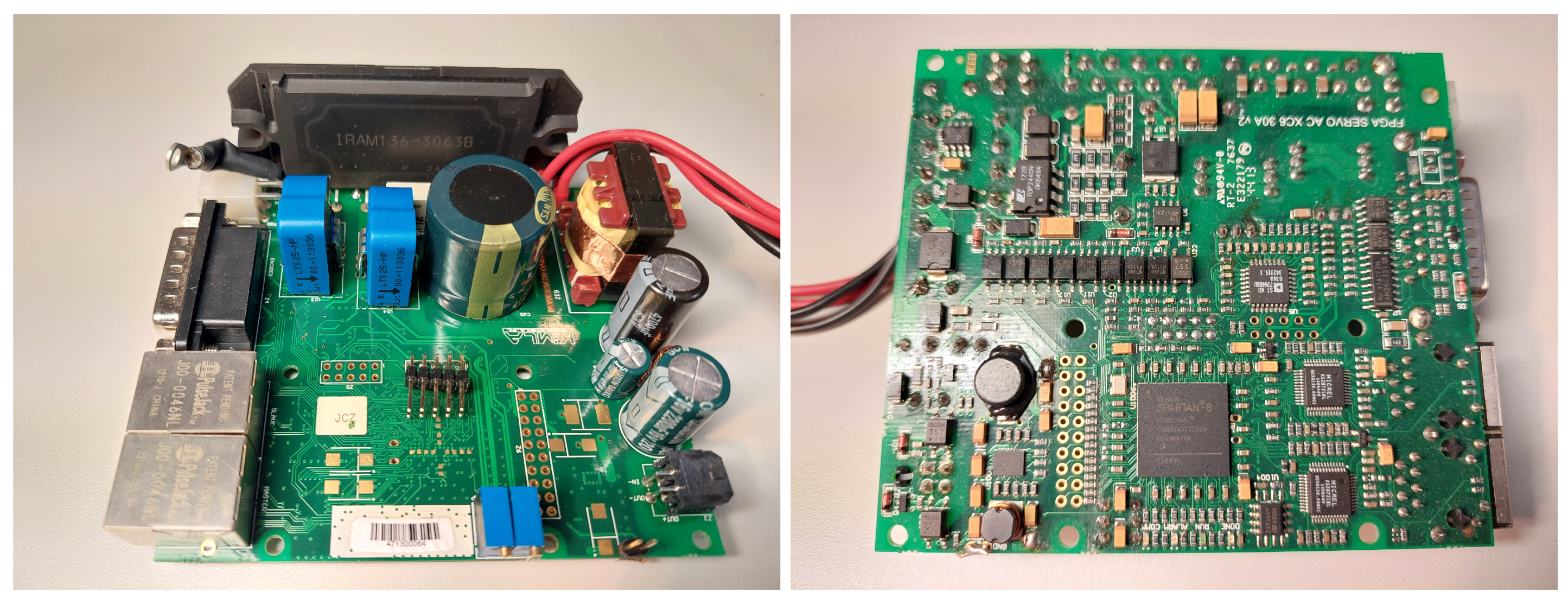
3.2. Properties and Architecture of an Electric Servo Drive Controller

If you look at the design of the electric servo drive controllers currently available on the market, you would notice that these devices are quite complex in terms of the digital part. For example, one of these controllers working with the EtherCAT real-time communication interface consists of as many as four PCBs with many ASICs and three digital signal processors mounted on them. These processors are designed to perform control tasks, real-time communication, and user interface, respectively. As you can guess, the dimensions, complexity, and the resulting cost of manufacturing such a controller are quite high.
An alternative to such a construction is the use of programmable digital circuits of the FPGA type. This approach reduces the complexity of the digital part and simplifies the controller PCB. This is because FPGAs allow the integration of many autonomous digital circuits such as ASIC, MCU, or DSP in their programmable structure. As a result, this usually leads to greater efficiency and better reliability, and potentially to lower production costs of the designed controller. Figure 4 shows photos of the PCB of an exemplary electric servo drive controller built based on an FPGA integrated circuit. As you can see, the complete controller fits on one PCB. The servo drive controller shown in the photos was used in the tests described later in this manuscript.
Figure 5 shows the structure of a classic electric servo drive control algorithm typically used in modern industrial machine tools. The controller of such a servo drive works with a permanent-magnet synchronous motor (PMSM) as well as with several sensors and actuators. Among them, the most important is the inverter controlled by six digital lines. These lines transmit high-speed, precisely generated pulse signals PA-T, PA-B, PB-T, PB-B, PC-T, and PC-B. These pulses are generated by a three-channel hardware PWM module based on the input signals P W M A / B / C . The generation of the above-mentioned pulse signals takes into account the required time interval (the so-called dead time) between the active states of the complementary signals of a given phase. This task, due to the required speed and time precision, cannot be performed by software.
All servo drive controller modules that, due to their specificity, must be fully supported by hardware have been marked in yellow in Figure 5. On the other hand, elements marked in green are those whose software implementation is possible, but the use of hardware acceleration in this area brings benefits in the form of significantly higher processing efficiency.
One of the main measuring elements used in the servo drive controller is the sensors of the electric current that flows through the motor windings. It is important that the measurement of the current in the windings of a three-phase motor must be performed simultaneously in two phases and must be precisely synchronized with the pulses generated by the PWM module. The measurement process is supervised by the hardware module marked in the figure as DUAL ADC INTERFACE.
Using several additional ADC channels, other analog values are also measured, i.e., the voltage V D C supplying the inverter and the temperature of several components of the controller.
In the servo drive, it is also necessary to precisely and quickly measure the position of the motor shaft. A suitable position sensor is used for this purpose. This sensor is connected to the controller using a specialized interface, e.g., qudrature encoder interface (QUAD), serial synchronous interface (SSI), or bidirectional serial synchronous (BISS). Interfaces of this type are used to communicate with various position sensors in machine tools or industrial robots [25]. The measurement of the position is therefore carried out via a specialized communication interface. Handling of pulse signals of this interface must be carried out with sufficiently high time precision, impossible to obtain by software implementation. This task is therefore handled by the hardware module of the controller marked in the diagram as BISS/QUAD.
For similar reasons, the implementation of the RTE interface, including solutions in standard or non-standard versions, should also be implemented in hardware. In this manuscript, the RTE solution is considered, the general idea of which is presented in work [26], while a detailed description can be found in work [1]. Detailed information regarding the implementation method of the RTE module is not relevant from the perspective of the analyzed issues in this study. However, the delay that occurs between the RTE hardware module (implemented on an FPGA or connected external ASIC) and the central processing unit is highly significant. For this reason, the description of the RTE module implementation is beyond the scope of this paper. As will be shown later, the integration of the RTE module inside the FPGA is one of the important elements affecting the high quality of the servo drive controller of the numerical machine tool.

3.3. Methods of Control Algorithm Implementation on FPGA

As mentioned earlier, the implementation of control algorithms on FPGAs based on the RTL design abstraction and the use of hardware description language is tedious, lengthy, and requires specialized knowledge. As a result, in many cases, designers of control systems refrain from the use of FPGAs [27] and choose solutions based on classic microcontrollers or signal processors and ASICs cooperating with them. Fortunately, in recent years, new methods have appeared that significantly facilitate and accelerate the process of implementing control systems on FPGAs. Interesting examples can be found in work [28] describing the methods of implementing PLC drivers on FPGAs. In addition, work [3] presents a classification of ways to implement control algorithms on FPGAs, indicating four possible methods for such implementation.
The first of these methods consists in describing the complete control algorithm using a hardware description language. This allows for a full hardware design (FHD) of such an algorithm and enables the highest possible processing efficiency. As indicated in [3], the disadvantage of such a solution, however, is the tedious and time-consuming design process, which also requires the designer to have highly specialized knowledge. This conclusion is quite obvious and consistent with what has already been written in this manuscript.
The next two methods presented in [3] were defined as soft-core-hardware function blocks (SC-HFB) and soft-core superscalar (SC-SS). Although these methods offer slightly lower efficiency than the FHD method, the efficiency is still high enough for applications such as those analyzed in this manuscript. Generally, both of the above-mentioned methods offer performance much higher than the software implementation marked in [3] with the symbol SC-CPU. The SC-CPU (soft-core CPU) method consists in implementing a control algorithm in the form of a C language code. This code was then executed by a universal soft-core processor, which was implemented on an FPGA.
As noted in [3], the most promising, from a practical point of view, method of implementing control algorithms on FPGAs is the SC-SS method. In this method, the implemented algorithm is described using low-level instructions similar in syntax to the assembler language of processors. These instructions explicitly describe the parallel operation of many basic execution units, which is characteristic of the very long instruction word (VLIW) [29,30] architecture. Individual instructions are encoded in the form of a very long binary word. The width of the command word is in the range from several dozen to several hundred and sometimes reaches even a thousand bits. In such an architecture, each instruction describes how multiple low-level execution units work. These units are dedicated to performing basic arithmetic and binary operations or to transferring data inside an integrated circuit. Each of these elementary execution units can perform its work in parallel with other units, thus contributing to the efficient processing of the implemented algorithm. In the SC-SS architecture presented in [3], the units that can work in parallel are fixed-point arithmetic units (multipliers, adders, subtractors, abs, min, max, clip, and compare) and data transfer units. The number and type of such units is a parameter of the system and, based on its scalability, is subject to adjustment to the requirements of a specific type of application.
According to the suggestion proposed in [3], such a method of hardware implementation of the algorithm can be conventionally referred to as very-low-level programming [31]. This name is justified especially when the number of low-level execution units is quite large and their degree of complexity is low. In this case, the software implementation on the SC-SS unit is somewhat similar to the structural design of FPGAs in hardware description languages. If, on the other hand, the number of low-level execution units is low, then the design is similar to the low-level programming of superscalar signal processors. However, it should be clearly stated, as will be shown later in this paper, that the SC-SS unit implemented on the FPGA offers much more flexibility. It is therefore possible to adjust the SC-SS unit to the requirements of the implemented class of algorithms, for example, control algorithms. As a result, the algorithm of a given class implemented on the SC-SS unit works faster than in the case of its implementation on the universal signal processor.
The SC-SS unit described below, based on the VLIW architecture, has been adapted to the specifics and requirements of applications in the broadly understood area of control systems. Such a match provides this unit with high performance and low demand for hardware resources of the FPGA. As a result, which will also be shown in the further part of the work, in the field of implementation of control algorithms, the general advantage of the solution based on FPGA and the SC-SS type unit compared to most other solutions is noticeable.
In work [3] it was shown that, as a result of using the SC-SS method, it is possible to implement a control algorithm with efficiency approximately ten times higher than the performance of an analogous algorithm implemented in software and executed by a soft-core processor. It is known, however, that soft-core processors offer significantly lower performance than analogous hard-core processors, including both those built into FPGA-SoC systems and autonomous processors. In the further part of this manuscript, it will be shown that, for a significant group of practical applications, the total efficiency of the control algorithm implemented on the SC-SS unit is also higher than the performance of the analogous algorithm implemented in software and executed by a hard-core processor. Two competitive digital platforms with hard-core processors will be analyzed, the first based on MCU and the second on DSP.
The experimental research performed concerns the implementation of the control algorithm (Figure 5) on three different digital platforms. Selected parameters of these platforms have been shown in Table 2.
The first platform is marked with the MCU symbol and is based on a 32-bit ARM Cortex-M4 microcontroller operating at 180 MHz [32]. This chip is equipped with a hardware floating-point unit (FPU). To support the RTE EtherCAT communication interface, this microcontroller cooperates with a dedicated integrated circuit (ASIC) with the symbol ET1100 EtherCAT Slave Controller [5] via a 16-bit parallel bus. The maximum supported operating frequency of this interface is 40 MHz, and the operation of writing or reading a 16-bit data word to/from the ASIC takes four clock cycles, i.e., 100 ns.
The second digital platform (DSP) on which experimental research was carried out is the Analog Devices ADSP21369 floating-point digital signal processor operating at 400 MHz [33]. This chip has been connected through a 32-bit parallel interface to the Microchip KSZ8842-32MQL 2-Port Ethernet Switch [34]. In this case, the operation of writing or reading a 32-bit data word to/from the ASIC takes 110 ns.
The third digital platform (FPGA) was built based on the FPGA chip with the symbol AMD Xilinx XC6SLX45-3 [17] produced in 45 nm technology (Figure 4). The SC-SS unit was implemented on this chip. The details of this implementation are described in the next subsection, as well as in the publication [3].
It should be noted that the research presented in the further part of this work does not cover all aspects related to the selection of a specific digital platform for a particular application. For example, issues related to the security protection of digital systems, including measures against actions such as reverse engineering, cloning, and tampering, were not taken into account. This paper rather focuses on topics related to the performance, energy consumption, and compactness of digital controllers.

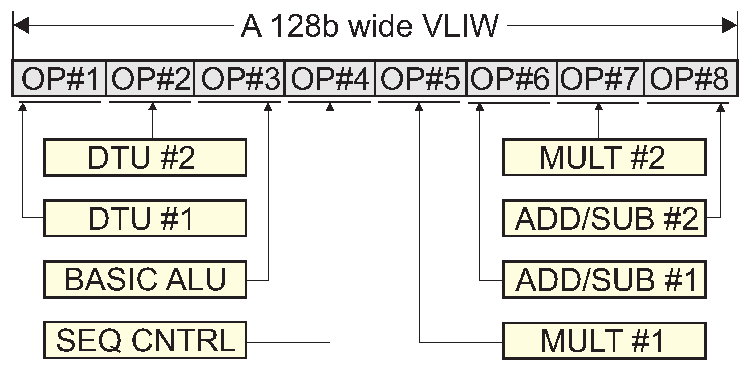
3.4. The Applied Soft-Core Superscalar Architecture

To understand some important issues described later in this paper, it is necessary to know the internal architecture of the SC-SS unit. The SC-SS unit is intended to be implemented in the FPGA system as a unit cooperating with a standard, universal soft-core processor (CPU). As part of such cooperation, the role of the CPU is to control the startup and configuration process of the system, its management and supervision, and the operation of the user interface. On the other hand, the role of the SC-SS is to implement control algorithms efficiently.
Figure 6 shows the internal architecture of the SC-SS unit and how it interacts with the CPU. The SC-SS includes sixteen universal registers marked as R0…R15 (FXU REGISTERS). Half of the registers (i.e., R0–R7) were realized as 32-bit words and were used to store signal values with a full resolution, while the other half of the registers (i.e., R8–R15) were realized as 16-bit words and were used to store the parameters of operations. Such an asymmetric structure of registers allows for a significant simplification of the hardware structure of the processing unit while maintaining the requirements of typical control algorithms.
The SC-SS also includes five elementary execution units (FX-AU #1…FX-AU #5) and two data transfer units (DTU #1 and DTU #2) used to transfer data between registers and two blocks of dual-port memory blocks (DP-RAM DATA #1 and DP-RAM DATA #2). Among the elementary execution units are two FX-MULT units and two FX-ADD/SUB units. FX-MULT units are capable of performing fixed-point multiplication along with scaling the result. The FX-ADD/SUB units perform fixed-point arithmetic addition or subtraction with scaling of one of the components. The last one of the FX-AUs performs simple universal integer arithmetic operations (BASIC ALU) useful in signal processing algorithms. These are MIN, MAX, NEG, and some simple binary operations. The SC-SS unit was designed in such a way that all elementary execution units and data transfer units have unlimited and simultaneous access to all FXU registers.
The SC-SS unit cooperates with the universal CPU, shown in the lower left part of the picture, by exchanging data using three dual-port memories visible in the upper left part of Figure 6. The DP-RAM #1 and DP-RAM #2 are used to exchange data constituting the input and output signals of the implemented control algorithm, whereas the memory block marked as DP-RAM PROGRAM stores binary codes of program instructions executed by the SC-SS unit. These instructions are written into memory by the CPU during the startup phase.
All elementary execution units (FX-AU #1…FX-AU #5) included in the SC-SS can work in parallel. They are controlled through 16-bit fields placed in the appropriate place in the binary word (Figure 7). Such a word (VLIW) has a length of 128 bits and is divided into eight control fields (OP#1–OP#8) that define the operations performed by individual modules of the SC-SS unit. The first two fields (OP#1 and OP#2) control the operation of the DTU #1 and DTU #2 units. The subsequent field controls the BASIC ALU unit. In turn, the SEQ CNTRL binary field defines the operation of the VLIW CODE SEQUENCER module visible in the Figure 6. The purpose of this module is to handle branches in the executed code and halt its execution after completing the computations. The four last fields of the VLIW word (OP#5–OP#8) define the operation of the elementary arithmetic processing units, namely, MULT #1, ADD/SUB #1, MULT #2, and ADD/SUB #2.
In general, it can be noticed that the internal architecture of the SC-SS unit shown on the right side of Figure 6 is very similar to that used in typical superscalar digital signal processors. However, there are some significant differences that will be presented in the subsequent part of this work. In particular, specific hardware mechanisms to accelerate the execution of certain algorithms and greater versatility in the parallel operation of elementary processing units should be mentioned. Detailed information about such specific hardware solutions will be presented later, along with a description of several selected instructions of the SC-SS unit.
The following is a list of the most important instructions of the SC-SS unit:
  • PolyInit n , m , A d d r —is a dedicated instruction for hardware acceleration of the LTSE algorithm. It implements the initialization of the n-th order LTSE with the division of the approximation domain into 2 m segments. The coefficients of the polynomials used in the approximation are listed in the two-dimensional array indicated as the last argument of the instruction.
  • M1_A A d d r —this is the operation of addressing the first of the two memory blocks to prepare for the read operation in the next clock cycle. The symbol Addr denotes the address of the variable placed in the M1 memory block. The corresponding instruction for the second memory block is labeled M2_A.
  • M1_RI R a —is the actual operation of reading from memory to the general register with the index a = 0 15 and simultaneous addressing of the next memory location by address increment. The corresponding instruction for the second memory block is M2_RI.
  • R o = R a R b ( i a , i b , i o ) 
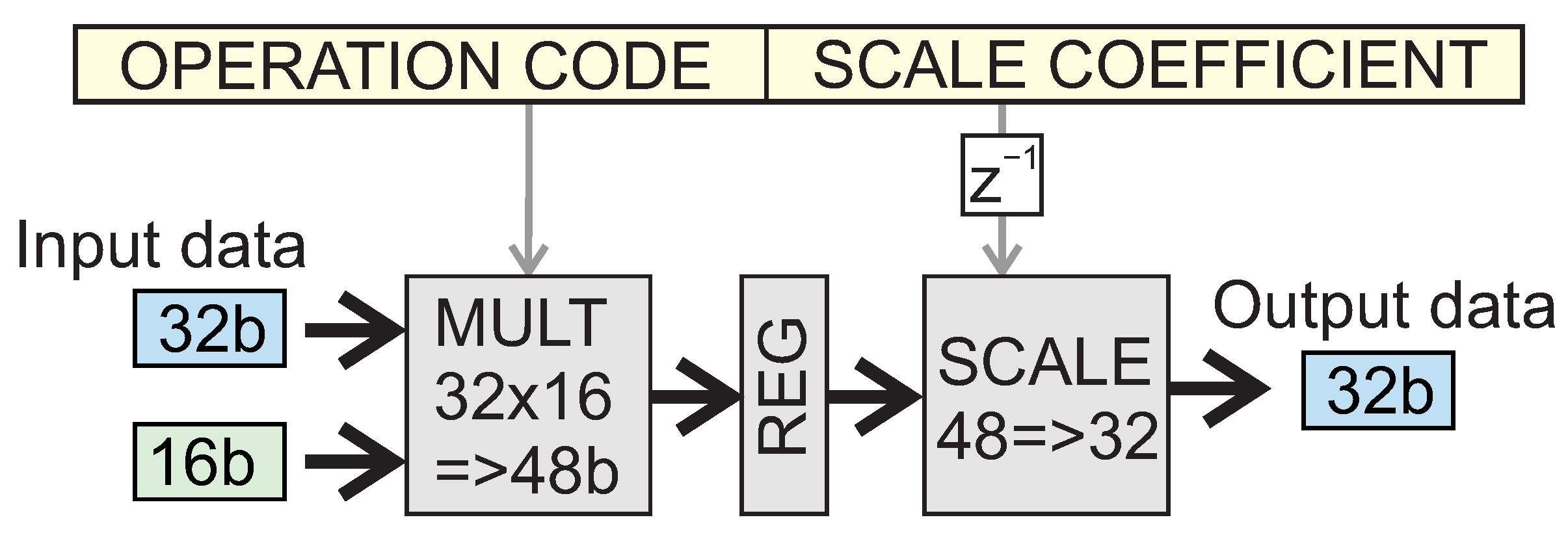
—fixed-point multiplication with scaling, where: a , b , o = 0 15 are the indexes of the universal registers identifying the first and second arguments and the result register, while i a , i b , i o are the i parameters defining the format of the processed fixed-point numbers, following the Fxi_n notation [3]. In this notation, the ‘i’ parameter describes the position of the binary point counting to the right, starting from the left side of the binary word. In the research described in this paper, 32-bit words were used to represent the values of processed signals. In this case, the value of n was 32. However, 16-bit words were used to represent constant parameters, so, in that case, the value of n was 16.
    This fixed-point multiplication is performed by the FX-MULT unit shown in Figure 8. The first part of the operation is integer multiplication, which results in a 48-bit number written to the internal register (REG) of the FX-MULT unit. To obtain the expected output format, this result will be shifted to the right by the number of positions expressed by Formula (1). This integer value is determined during the code compilation stage and placed in the SCALE COEFFICIENT field of the binary instruction intended to be executed by the FX-MULT unit.
    s M = ( 32 i a ) + ( 16 i b ) ( 32 i o )
  • R a + = R b ( i a , i b ) 
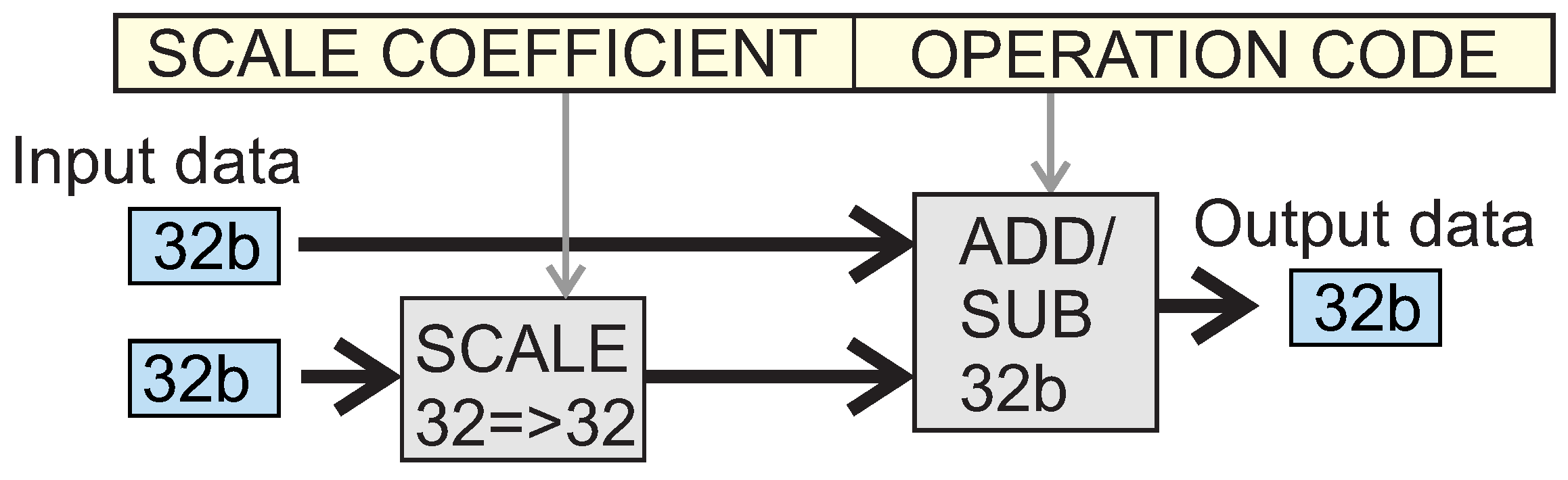
—these are integer addition operations where the second argument is automatically scaled to the format of the first argument. The subtraction operation looks similar. This operation is shown in Figure 9 and has the predetermined requirement that i a i b . In this case, the “SCALE COEFFICIENT” field contained in the code of the instruction describes the binary left shift value. This value is determined by Formula (2) at the code compilation stage.
    s A = i a i b .
All elementary operations are performed by the SC-SS unit in a single clock cycle. The only exception is the integer multiplication instruction with scaling. In this case, the result of the multiplication is available only after two clock cycles. The SC-SS unit performing a two-cycle operation does not control the readability of the result. The programmer designing the VLIW code of the SC-SS unit must take care not to access the result register of the FX-MULT unit before two clock cycles have elapsed. According to what was presented in publication [3], this feature introduces some difficulty for the designer of the VLIW code but at the same time simplifies the construction of the SC-SS unit implemented on the FPGA. As a result, it can work more efficiently on a given hardware platform, which is consistent with the general concept presented in publication [35].
For such an implementation, the consumption of FPGA hardware resources is 14,799 LUTs (54%), 14 DSP48E1s (24%), and 113 RAMB16WERs (97%).

3.5. Algorithm Implementation Details

The SC-SS unit implemented on the FPGA works with a clock frequency of 80 MHz. It is used to execute the code that implements the control algorithm blocks marked in green in Figure 5. In addition to the SC-SS unit, other hardware blocks have also been implemented on the FPGA, which are marked in yellow in Figure 5. As already mentioned, among them there is a unit that processes four 4-bit data streams in the media-independent interface (MII) standard, used for RTE communication. These streams are transmitted at a frequency of 25 MHz and are used to communicate with two integrated circuits of the Ethernet physical layer (PHY). The Ethernet PHYs are visible in the bottom right corner of Figure 4. Because the FPGA can directly process data streams of the MII interface, i.e., it does not require additional ASICs for this purpose, delays in data transfer via the RTE interface are reduced to a minimum.
For both platforms with hard-core processors (i.e., MCU and DSP), the control algorithm is implemented in the C language and is performed by an adequate central processing unit (CPU). In the case of the SC-SS unit, the algorithm was implemented based on manually coded VLIW instructions [3]. The VLIW code designed in this way is executed by the SC-SS unit implemented on the FPGA.
In Table 3 in rows 2–5, the results of the implementation of selected functional blocks of the algorithm shown in Figure 5 are shown. The first column describes the name of the implemented block, while the subsequent columns identify the hardware platform on which this code was implemented and tested. The results given in the table present the processing time of individual code fragments. All algorithm blocks presented in this table must be run every cycle of the controller’s operation. It is therefore essential that these blocks are executed quickly enough. Therefore, the lower the value given in the table, the better.
The row of the table marked as “Sine and cosine”, concerns a fragment of the algorithm responsible for determining the values of the sine and cosine functions. These values are necessary for the operation of the vector control algorithm of the servo drive [21] and in particular for space-vector modulation (SVM). The next row of the table concerns the implementation of the Clarke and Park algorithms in the normal and inverse versions, together with the compensation of supply voltage ripples. In turn, the row of the table marked “Dual-channel PI” concerns the implementation of two proportional-integral (PI) controllers used to control two components of the space vector representing the electric current of the motor. The penultimate row of the table represents the time of transfer of two different data portions (28 B and 256 B) between the hardware unit realizing RTE communication and the central processing unit CPU, i.e., MCU, DSP, or SC-SS, for the analyzed cases.
The sizes of both data portions included in the table result from the requirements of the implemented control algorithm and the implementation of additional service functions. The 28 B data portion represents the basic set of input and output signals processed in each work cycle by the algorithm implemented on the controller. On the other hand, a chunk of data of 256 bytes represents a case where the controller sends or receives additional data streams. Such data is used, among other things, for service purposes, i.e., to analyze the internal signals of distributed controllers and to perform other functions of the machine control system [1].
It should be noted that the transfer rate of this data depends not only on the speed of the CPU interface but also on the interface limitations of the peripheral ASIC. General information about these limitations has been given earlier in this chapter. As you can see from the data presented in the table, the transfer time of individual packets for platforms marked as MCU and DSP is quite high. On the other hand, in the case of the FPGA system, the transfer time of such data is negligible, as it concerns the operation of copying data between independent memory blocks of the same integrated circuit.
For the sake of clarity, only some elements of the complete servo drive control algorithm are presented in Table 3. Among other things, the feedforward paths of the control signals, and the position and speed regulators were omitted. The engine speed estimation block, and elements related to the configuration of the controller and its adjustment to various operating modes have also been omitted. Therefore, the total calculation times presented in the last row of the table should be treated only as a fragment of the total processing time of the complex algorithm implemented on the controller.
The method of conducting experimental research was slightly different for individual digital platforms, which resulted from technical reasons. In the case of the MCU platform, the implemented algorithms (shown in Table 3) were run on the evaluation board. The processing time of these algorithms was measured using a digital oscilloscope. On the other hand, communication delays between the MCU and the ASIC were calculated on the basis of the manufacturer’s documentation. Similarly, the power consumption (included in Table 2) of the microcontroller and the ASICs attached to it, i.e., one ET1100 chip and two Ethernet physical layer integrated circuits, was estimated.
Research on the DSP platform was carried out on a controller that is part of the real control system of a numerical machine tool. All measurements regarding the processing time of the algorithms, as well as delays in communication with the ASIC, were carried out using a digital oscilloscope. The electrical power consumption was measured using a digital multimeter. The result of this measurement includes the power consumed by the DSP, by the ASIC, and by the external SDRAM memory necessary for the operation of the DSP.
The platform marked as FPGA is also a controller (Figure 4) that is part of the real control system of the numerical machine tool. All measurements regarding the processing time of the algorithms, as well as delays in communication with the RTE module, were carried out using a digital oscilloscope. The electrical power consumption was measured using a digital multimeter. The result of this measurement includes the power consumed by the FPGA and the two Ethernet physical layer integrated circuits.
Further in this section, an analysis of the implementation of the approximation algorithm, abbreviated as LTSE, will be presented. As before, the results of such an implementation on various digital platforms will be compared. This analysis will make it possible to highlight some important features of individual platforms and better understand the results presented in Table 3.
LTSE is an approximation algorithm that combines a look-up table mechanism and Taylor series expansion. More detailed information is provided in publication [3]. The LTSE algorithm is used to approximate the values of any continuous, non-linear functions of one variable. In general, the LTSE algorithm, like any approximation algorithm, offers a compromise between the speed and precision of calculations. In the case of the numerical machine tool control system analyzed in this manuscript, this algorithm may be useful in several places. For example, it can be used to approximate the value of the square root, arithmetic inverse, or the sine and cosine functions, which are necessary for the operation of the analyzed control system. The use of approximations of such functions instead of determining their precise values based on available mathematical libraries allows for a significant reduction in the processing time of the implemented control algorithm. The approximation of computationally expensive functions is an important and current issue in the field of embedded systems design. An example of another approach to approximation of such functions is proposed in publication [36]. On the other hand, in paper [37] it was shown that the use of fixed-point arithmetic in many practical cases brings a significant reduction in computation time in comparison to the use of floating-point arithmetic.
Table 3 shows the results for approximating the sine and cosine functions. The method of implementing the code for individual digital platforms has been selected in such a way as to ensure the highest possible efficiency with the required precision and acceptable level of complexity. Implementation details have therefore been tailored to the specific features of each platform. In addition, the code was compiled with the maximum available optimization level of the given compiler. For example, in the case of the implementation of the “Sine and cosine” block on the MCU, ready-made functions “sinf” and “cosf” from the mathematical library <math.h> of the integrated development environment STM32CubeIDE version 1.12.0 were used. They turned out to be well optimized for the given platform and offered slightly better performance than the C implementation of the LTSE algorithm. The opposite was the case with the implementation of the above-mentioned functional block on the DSP. In this case, the C code implementing the LTSE algorithm turned out to be slightly faster than the functions from the standard math library. As mentioned earlier, the table shows the best possible results for each platform.
In the analyzed case, i.e., the implementation of the sine function, the LTSE 5-th order method was used with the division of the domain into eight segments [3]. The algorithm for calculating the polynomial value was based on Horner’s scheme and is shown in Listing 1. An analogous code has also been implemented on the SC-SS unit operating on the FPGA chip, the detailed construction of which is described in publication [3]. This code is presented in the form of instructions in Listing 2.
Listing 1. Fragment of C-code for LTSE algorithm implementation on a DSP unit.
1#define POLY_ORDER 5
2float LTSE_sin ( float x )
3{
4unsigned int segIndex ;
5/* Convert to integer format and use the three
6most significant bits as the segment index . */
7 segIndex = x * ONE_OVER_TWO_PI_FX1_16 ;
8 segIndex = ( segIndex >> 13) & 0x0007u ;
9/* The Horner ’ s scheme . */
10float sum = LTSE_Coeff [ segIndex ] [ 0 ] ; // y0
11 x −= LTSE_Coeff [ segIndex ] [ 0 ] ;
12int i ;
13for ( i=POLY_ORDER; i >=1; i −−)
14 {
15  sum = sum ∗ x + LTSE_Coeff [ segIndex ] [ i ] ;
16 }
17return sum;
18}
Listing 2. Fragment of FXU code for LTSE algorithm implementation on SC-SS unit.
1PolyIni t 5 , 3 , LTSE_Coeff ; M1_A x ;
2M1_RI R0 ; // Load the argument and calculate the segment index .
3M2_RI R6 ; // Load the value of x0 .
4R0 −= R6 ; // Calculate the value of z .
5R3 = R0R0 ( 2 , 2 , 2 ) ; M2_RI R7 ; // Calculate the value of z^2 and load the value of y0 .
6R1 = R0 ; R2 = R0 ; M2_RI R8 ; // Load the value of C1 .
7R4 = R1R8 ( 2 , 2 , 2 ) ; R1 = R1R3 ( 2 , 2 , 2 ) ; M2_RI R8 ; // Use C1 , load C2
8R5 = R2R8 ( 2 , 2 , 2 ) ; R2 = R2R3 ( 2 , 2 , 2 ) ; M2_RI R8 ; // Use C2 , load C3
9R7 += R4 ( 2 , 2 ) ; R4 = R1R8 ( 2 , 2 , 2 ) ; R1 = R1R0 ( 0 , 2 , 2 ) ; M2_RI R8 ; // Use C3 , load C4
10R7 += R5 ( 2 , 2 ) ; R5 = R2R8 ( 2 , 0 , 2 ) ; R2 = R2R0( −2 , 0 , 2 ) ; M2_RI R8 ; // Use C4 , load C5
11R7 += R4 ( 2 , 2 ) ; R4 = R1R8( 2 , −2 , 2 ) ; // Use C5
12R7 += R5 ( 2 , 2 ) ;
13R7 += R4 ( 2 , 2 ) ; // Result is in register R7 .

3.6. Analysis of the Obtained Results

In Listing 2, units working in parallel are shown as groups of instructions on the same line. Each such single line represents one digital word of the VLIW code executed by the SC-SS unit. The complete LTSE algorithm implemented on the above-described SC-SS unit requires only thirteen clock cycles, which is equivalent to 162 ns, to compute the result. However, in Table 3 this result is visible in the row “Sine and cosine” in the column marked “FPGA” as the value 0.31 μ s. This value results from calling this algorithm twice to determine both sine and cosine values.
An analogous algorithm implemented in the C language and running on a DSP processor with RISC (Super-Harvard ARChitecture, SHARC) architecture takes as many as 46 clock cycles. The DSP processor used in the experiment works with a clock frequency of 400 MHz, so the execution time of a single instruction is only 2.5 ns. The execution time of the entire LTSE algorithm is therefore 115 ns. As before, the table shows the total computation time for the sine and cosine functions, which is 0.23 μ s. This indicates that, despite the DSP operating at a clock frequency five times higher than the SC-SS unit implemented on FPGA, the performance of the LTSE algorithm executed by the DSP was only slightly higher. There are two reasons for this result.
First of all, according to the analysis of the low-level code of the DSP processor (this code was generated by the C compiler), almost 30% of the processor time (13 clock cycles) is spent initializing the LTSE algorithm. The analyzed fragment of the C code is represented by lines 1–8 of Listing 1. The initialization process of the LTSE algorithm consists of operations such as determining the index of the expansion segment, addressing the block of memory storing the coefficients of the series for the designated segment, and rescaling the argument of the approximated function. These are universal operations for which the DSP is not dedicated, resulting in the long processing time of this part of the code. In the case of the SC-SS unit, the initialization of the LTSE algorithm takes only four clock cycles, which is represented by lines 1–4 of Listing 2. The excellent performance of the SC-SS unit is primarily the result of utilizing a hardware mechanism that accelerates the operation of the LTSE algorithm. This mechanism is triggered by the ’PolyInit’ instruction.
Secondly, the SC-SS unit offers significantly better parallel processing capabilities compared to the DSP. As shown in Listing 2, within multiple sections of the code (lines 7–10), even three or four elementary execution units work in parallel. These are code fragments that perform the computation of polynomial values based on the Horner scheme. In contrast, in the case of the DSP processor, at most two such units worked in parallel.
The analysis shows that the mechanisms of the SC-SS unit, thanks to which such good results were obtained, are primarily: (a) a dedicated hardware initialization mechanism for the LTSE algorithm and (b) a superscalar execution unit with high parallel computing capabilities. It should be noted that it is possible to adapt the SC-SS unit to efficiently implement many different types of algorithms. This is possible because this unit is implemented in the programmable logic of the FPGA. Other hardware platforms such as MCU or DSP do not offer such flexibility and therefore, despite a much higher frequency of operation, do not offer the expected performance.
The results of experimental research presented in Table 3 provide confirmation of the high performance of the proposed solution. Additionally, the comparison of the advantages and disadvantages of individual solutions has been included in Table 4. Among the data contained in the table, there is information that solutions based on FPGAs offer large development potential. This is due to the ability to match the hardware mechanisms implemented in the FPGA to the efficient processing of various innovative algorithms. This is a very important advantage of the FPGA-based solution.
The evaluation of the obtained results can be conducted by checking whether the stated goals have been achieved. Additionally, the answers to research questions resulting from the studies are essential. According to the title of the paper, the aim of conducting the research was the optimization of numerical machine tool servo drives. The research question concerned the possibility of achieving this aim by using FPGA technology in such controllers. Optimization of servo drives entails improving one or more of their defining characteristics, such as enhancing motor control precision, obtaining new functionalities, or reducing manufacturing costs. As indicated at the beginning of the paper, to enhance precision and add new functionalities (related to servicing and control system development), it is necessary to increase the processing performance of the utilized computing unit. On the other hand, although there are sometimes controllers with sufficient computing power, their high manufacturing cost and large size can be considered significant drawbacks. Therefore, the improvement of at least one parameter describing a particular controller without significantly worsening others can be understood as its multi-criteria optimization.
As indicated by the results presented in the last row of Table 3 and in Table 2, the application of the proposed solutions led to an improvement in several parameters of the servo-drive controller, while one parameter showed a slight deterioration. Specifically, according to the data in the last row of Table 2, the approximate cost of key digital elements is slightly higher for the FPGA platform compared to other platforms, which can be considered a drawback. However, the overall processing performance of the FPGA platform was significantly higher than other platforms when considering the case requiring increased data transfer between controllers. Secondly, the power consumption was reduced compared to the competitive solution with a DSP processor. Although the microcontroller-based solution has the lowest power consumption, it offers the lowest performance. Thirdly, the complexity and, consequently, the size of the electronic printed circuit board in the FPGA-based solution is lower than in the other analyzed solutions. This is due to a smaller number of integrated circuits that need to be mounted on it.
However, regardless of such understanding of the optimization process, it is also crucial for each parameter of the considered system to meet its minimum requirements. In the case analyzed in this study, one of the significant objectives was to add new functionality to the control system by transmitting a larger amount of data between controllers. To achieve this effect, it is necessary to increase the processing performance of the digital controllers. However, a specific value by which this performance should be increased was not provided in the assumptions. As indicated at the beginning of the paper, the higher the throughput and the lower the delay of the RTE interface, while maintaining its full-time regime, the better the parameters of the control system that can be obtained. As indicated by the research results presented in the last row of Table 3, such an objective was achieved based on the solutions proposed in this paper.

4. Conclusions

In this manuscript, new solutions in the field of control systems for industrial CNC machines have been presented. In particular, the author’s contributions in this area include:
  • Description of the architecture, specific features, and requirements imposed on control systems of modern industrial CNC machines.
  • Identifying areas where the control system can be developed to improve machining precision, introduce new functionalities, and enhance diagnostic and service operations.
  • Diagnosis of the limitations of controllers typically used in servo drives based on microcontrollers or signal processors collaborating with application-specific integrated circuits (ASICs) regarding the feasibility of implementing the proposed new solutions.
  • Designing and implementing a solution based on FPGA technology to eliminate the above-mentioned limitations. This solution involves proper configuration and utilization of the SC-SS unit for hardware–software processing of the servo drive control algorithm, as well as integrating the SC-SS unit and the RTE module within a common FPGA structure.
  • Designing and conducting comprehensive experimental studies on three distinct digital platforms. Two of the evaluated platforms are integrated into the control systems of existing CNC machines available in the commercial market. The tests conducted on these platforms exhibit high reliability due to their execution under real operational conditions of the machine tool control system.
  • Conducting a rigorous analysis of the obtained results, considering the achieved processing efficiency of the controllers, real-time communication interface delays, the amount of consumed electrical power, the complexity of the electronic printed circuit board, and the cost of digital components.
The proposed new solutions meet all the requirements imposed on control systems of modern machine tools, particularly providing high computational power at a low cost. This enables the implementation of advanced algorithms required to control modern machines. Additionally, the high performance of the RTE interface provided by the proposed solution significantly facilitates the analysis of the entire control system’s operation. A large number of internal signals from individual controllers can be conveniently recorded in real time during normal machine operation. This leads to improved automatic machine diagnostics and potential servicing processes.
The analysis and experimental research conducted in this manuscript confirm the benefits of using FPGA circuits in control systems of industrial CNC machines. Moreover, FPGA applications can bring similar benefits to control systems of other types of machines, devices, or processes.
The proposed solutions are naturally suited to control systems of various types of machines, industrial robots, and vehicles, i.e., generally motion control systems. The greatest benefits will be observed in systems that require high precision at high speeds. However, the potential application area of the developed solutions is much broader, as it generally covers control systems for any fast-changing processes.

Funding

The project was financed under the program of the Polish Minister of Science and Higher Education under the name “Regional Initiative of Excellence” in the years 2019–2023 project number 020/RID/2018/19; the amount of financing was PLN 12,000,000.

Data Availability Statement

No new data were created or analyzed in this study. Data sharing is not applicable to this article.

Conflicts of Interest

The author declares no conflict of interest.

References

  1. Przybył, A. Hard real-time communication solution for mechatronic systems. Robot. Comput.-Integr. Manuf. 2018, 49, 309–316. [Google Scholar] [CrossRef]
  2. Kimla, P. The Advantage of Fiber Lasers. Available online: https://kimla.pl/en/technical/the-advantage-of-fiber-lasers (accessed on 7 April 2021).
  3. Przybył, A. Fixed-Point Arithmetic Unit with a Scaling Mechanism for FPGA-Based Embedded Systems. Electronics 2021, 10, 1164. [Google Scholar] [CrossRef]
  4. Rutkowski, L.; Przybyl, A.; Cpalka, K. Novel Online Speed Profile Generation for Industrial Machine Tool Based on Flexible Neuro-Fuzzy Approximation. IEEE Trans. Ind. Electron. 2012, 59, 1238–1247. [Google Scholar] [CrossRef]
  5. Beckhoff. Hardware Data Sheet. EtherCAT Slave Controller. 2017. Available online: https://www.beckhoff.com/en-en/products/i-o/ethercat-development-products/elxxxx-etxxxx-fbxxxx-hardware/et1100.html (accessed on 7 April 2023).
  6. Schumacher, M.; Jasperneite, J.; Weber, K. A new Approach for Increasing the Performance of the Industrial Ethernet System PROFINET. In Proceedings of the 7th IEEE International Workshop on Factory Communication Systems (WFCS 2008), Dresden, Germany, 21–23 May 2008; pp. 159–167. [Google Scholar]
  7. Ogawa, T. Reduce BOM Costs and Development Efforts for EtherCAT and Other Industrial Ethernet-Compatible Servo Systems. 2023. Available online: https://www.renesas.com/us/en/document/whp/reduce-bom-costs-and-development-efforts-ethercat-and-other-industrial-ethernet-compatible-servo (accessed on 7 April 2023).
  8. Maneesh, S. EtherCAT® on Sitara™ Processors. 2020. Available online: https://www.ti.com/lit/pdf/spry187 (accessed on 7 April 2023).
  9. Unpatchable Cyber-Flaws Found on over 120 Siemens PLCs. Available online: https://drivesncontrols.com/news/fullstory.php/aid/7224/Unpatchable_cyber-flaws_found_on_over_120_Siemens_PLCs.html (accessed on 7 April 2023).
  10. Heinz, A. Obsolescence Risks Persist! Available online: https://www.elektroniknet.de/international/obsolescence-risks-persist.204469.html (accessed on 7 April 2023).
  11. Chiang, J.; Zammattio, S. Five Ways to Build Flexibility into Industrial Applications with FPGAs, White Paper WP-01154-2.2. 2014. Available online: https://www.intel.com/content/dam/www/programmable/us/en/pdfs/literature/wp/wp-01154-flexible-industrial.pdf (accessed on 7 April 2023).
  12. Tao, F.; Tang, Y.; Zou, X.; Qi, Q. A field programmable gate array implemented fibre channel switch for big data communication towards smart manufacturing. Robot. Comput.-Integr. Manuf. 2019, 57, 166–181. [Google Scholar] [CrossRef]
  13. What Is Software Defined Everything—Part 1: Definition of SDx. 2016. Available online: https://www.sdxcentral.com/cloud/definitions/software-defined-everything-sdx-part-1-definition/ (accessed on 7 April 2023).
  14. Haddad, S. Why a Software-Defined Approach Is the Future for Embedded and IoT. 2023. Available online: https://www.embedded.com/why-a-software-defined-approach-is-the-future-for-embedded-and-iot/ (accessed on 7 April 2023).
  15. High-Speed, Low-Cost Telemetry Access from Space (MFS-TOPS-62). Programmable, Lightweight, and Adaptable Software-Defined Radio. Available online: https://technology.nasa.gov/patent/MFS-TOPS-62 (accessed on 7 April 2023).
  16. Diverse Architectures for Unmatched Innovation. Available online: https://www.intel.com/content/www/us/en/silicon-innovations/6-pillars/architecture.html (accessed on 7 April 2023).
  17. Xilinx. Xilinx Spartan-6 Family Overview, DS160. 2011. Available online: https://docs.xilinx.com/v/u/en-US/ds160 (accessed on 7 April 2023).
  18. AMD Adaptive SoCs. Available online: https://www.xilinx.com/products/silicon-devices/soc.html (accessed on 7 April 2023).
  19. Sankar, D.; Syamala, L.; Chembathu Ayyappan, B.; Kallarackal, M. FPGA-Based Cost-Effective and Resource Optimized Solution of Predictive Direct Current Control for Power Converters. Energies 2021, 14, 7669. [Google Scholar] [CrossRef]
  20. Scrugli, M.A.; Meloni, P.; Sau, C.; Raffo, L. Runtime Adaptive IoMT Node on Multi-Core Processor Platform. Electronics 2021, 10, 2572. [Google Scholar] [CrossRef]
  21. Przybył, A.; Szczypta, J. Method of Evolutionary Designing of FPGA-based Controllers. Przegląd Elektrotechniczny 2016, 92, 174–179. [Google Scholar] [CrossRef]
  22. Nowak, M.; Popenda, A. Influence of neural network configuration on PMSM motor angular velocity estimation. Przegląd Elektrotechniczny 2023, 99, 238–241. (In Polish) [Google Scholar] [CrossRef]
  23. Dziwiński, P.; Avedyan, E.D. A New Method of the Intelligent Modeling of the Nonlinear Dynamic Objects with Fuzzy Detection of the Operating Points. In Artificial Intelligence and Soft Computing; Rutkowski, L., Korytkowski, M., Scherer, R., Tadeusiewicz, R., Zadeh, L.A., Zurada, J.M., Eds.; Springer International Publishing: Cham, Switzerland, 2016; pp. 293–305. [Google Scholar] [CrossRef]
  24. Dziwinski, P.; Przybyl, A.; Trippner, P.; Paszkowski, J.; Hayashi, Y. Hardware Implementation of a Takagi-Sugeno Neuro-Fuzzy System Optimized by a Population Algorithm. J. Artif. Intell. Soft Comput. Res. 2021, 11, 243–266. [Google Scholar] [CrossRef]
  25. BiSS Interface Concept. 2021. Available online: https://biss-interface.com/download/biss-c-interface-flyer/ (accessed on 7 April 2023).
  26. Przybył, A.; Smoląg, J.; Kimla, P. Distributed Control System Based on Real Time Ethernet for Computer Numerical Controlled Machine Tool. Przegląd Elektrotechniczny 2010, 86, 342–346. (In Polish) [Google Scholar]
  27. Herasymenko, P. Software implementation of pulse-density modulation control for H-bridge series-resonant converters. Przegląd Elektrotechniczny 2023, 99, 116–119. [Google Scholar] [CrossRef]
  28. Hajduk, Z.; Trybus, B.; Sadolewski, J. Architecture of FPGA Embedded Multiprocessor Programmable Controller. IEEE Trans. Ind. Electron. 2015, 62, 2952–2961. [Google Scholar] [CrossRef]
  29. Fisher, J.A. Very Long Instruction Word Architectures and the ELI-512. In Proceedings of the 10th Annual International Symposium on Computer Architecture, ISCA ’83, Stockholm, Sweden, 13–17 June 1983; Association for Computing Machinery: New York, NY, USA, 1983; pp. 140–150. [Google Scholar] [CrossRef]
  30. Nurmi, J. Processor Design. System-on-Chip Computing for ASICs and FPGAs; Springer: Berlin/Heidelberg, Germany, 2007; Book Chapters 3 and 7. [Google Scholar] [CrossRef]
  31. Jenner, A. Reenigne Blog, Stuff I Think about, “Very Low-Level Programming”. Available online: https://www.reenigne.org/blog/very-low-level-programming/ (accessed on 12 April 2021).
  32. STMicroelectronics. RM0090 Reference Manual, Rev. 19. 2021. Available online: https://www.st.com/resource/en/reference_manual/rm0090-stm32f405415-stm32f407417-stm32f427437-and-stm32f429439-advanced-armbased-32bit-mcus-stmicroelectronics.pdf (accessed on 7 April 2023).
  33. Analog Devices, Inc. One Technology Way. In SHARC Processor Programming Reference, Rev. 2.4; Analog Devices, Inc.: Wilmington, MA, USA, 2013. [Google Scholar]
  34. Micrel. KSZ8842-16/32 2-Port Ethernet Switch with Non-PCI Interface. Data Sheet. 2007. Available online: https://www.microchip.com/content/dam/mchp/documents/OTH/ProductDocuments/DataSheets/KS8842M.pdf (accessed on 7 April 2023).
  35. Hennessy, J.; Jouppi, N.; Przybylski, S.; Rowen, C.; Gross, T.; Baskett, F.; Gill, J. MIPS: A Microprocessor Architecture. SIGMICRO Newsl. 1982, 13, 17–22. [Google Scholar] [CrossRef]
  36. Istoan, M.; Pasca, B. Fixed-Point Implementations of the Reciprocal, Square Root, and Reciprocal Square Root Functions. 2015. Available online: https://hal.archives-ouvertes.fr/hal-01229538/document (accessed on 12 April 2021).
  37. Sandoval-Hernandez, M.; Velez-Lopez, G.; Vazquez-Leal, H.; Filobello-Nino, U.; Morales-Alarcon, G.; De-Leo-Baquero, E.; Bielma-Perez, A.; Sampieri-Gonzalez, C.; Perez-Jacome Friscione, J.; Contreras-Hernandez, A.; et al. Basic Implementation of Fixed-Point Arithmetic in Numerical Analysis. Int. J. Eng. Res. Technol. 2023, 12, 313–318. [Google Scholar]
Figure 1. Modern industrial machine tools: (a) HSM milling machine, (b) WaterJet cutter and (c) laser fiber cutter.
Electronics 12 03585 g001
Figure 2. The structure of a distributed control system based on the RTE solution.
Electronics 12 03585 g002
Figure 3. Appearance and architecture of a typical FPGA device.
Electronics 12 03585 g003
Figure 4. Photos of a compact electric servo drive controller built on the basis of the FPGA system.
Electronics 12 03585 g004
Figure 5. Block diagram of the electric servo drive controller.
Electronics 12 03585 g005
Figure 6. Internal architecture of the applied SC-SS unit.
Electronics 12 03585 g006
Figure 7. Description of the functions of individual fields of the 128-bit instruction word in the proposed configuration of the SC-SS unit.
Electronics 12 03585 g007
Figure 8. Internal architecture of the FX-MULT unit.
Electronics 12 03585 g008
Figure 9. Internal architecture of the FX-ADD/SUB unit.
Electronics 12 03585 g009
Table 1. Basic parameters of selected Xilinx “6 series” FPGAs.
FPGA Part NumberDSP SlicesCLB SlicesBRAMsApprox. Price [USD]
XC6SLX91614303230
XC6SLX45586822116110
XC6SLX15018023,038268400
XC6VLX240T76837,6808324k
XC6VSX475T201674,400212820k
Table 2. Selected parameters of tested hardware platforms.
Selected ParametersMCUDSPFPGA
The amount of consumed electrical power [W] 1.2 2.4 1.4
Approximate cost of the key digital components [USD]6091120
Table 3. Processing time of selected fragments of the servo drive control algorithm implemented on various digital platforms. A lower value means higher performance.
Servo Code Functional BlockMCUDSPFPGA (SC-SS)
Sine and cosine1.18 μs0.23 μs0.31 μs
Clarke and Park0.33 μs0.09 μs0.18 μs
Inv. Park and SVM0.84 μs0.21 μs0.61 μs
Dual-channel PI0.98 μs0.30 μs0.48 μs
Data transfer delay 28 B/256 B1.40 μs/12.80 μs0.77 μs/7.04 μs0.10 μs/0.81 μs
The sum of the above 28 B/256 B4.73 μs/16.13 μs1.60 μs/7.87 μs1.68 μs/2.39 μs
Table 4. Advantages and disadvantages of using FPGAs in control systems for industrial numerical machine tools [3,28].
FeaturesMCU/DSP + ASICsFPGA
Processing performance (total)medium to highhigh (SC-SS) to very high (FHD)
Design comforthighlimited (SC-SS) low (FHD)
Compactness of the devicenoyes
Development potentiallimitedlarge
Disclaimer/Publisher’s Note: The statements, opinions and data contained in all publications are solely those of the individual author(s) and contributor(s) and not of MDPI and/or the editor(s). MDPI and/or the editor(s) disclaim responsibility for any injury to people or property resulting from any ideas, methods, instructions or products referred to in the content.

