Article

Phase-Shifted Energy Balance Control for Multilevel Inverters in Grid-Connected PV Systems

1
School of Marine Engineering, Guangzhou Maritime University, Guangzhou 510700, China
2
School of Electrical Engineering, Chongqing University of Science and Technology, Chongqing 401331, China
*
Author to whom correspondence should be addressed.
These authors contributed equally to this work.
Electronics 2023, 12(12), 2582; https://doi.org/10.3390/electronics12122582
Submission received: 28 March 2023 / Revised: 26 April 2023 / Accepted: 24 May 2023 / Published: 8 June 2023

Abstract

:
Cascaded multilevel converters are promising candidates for grid-connected PV systems, but low-frequency ripples may exist in a DC link. Such ripples are not just inherent; they can occur due to environmental factors, such as variations in a certain range of irradiance of the PV. To address this issue, this article proposes a clock phase-shifted (CPS) energy balance control method for grid-connected cascaded multilevel inverters for photovoltaic (PV) systems. The proposed control scheme can prevent the low-frequency ripple of the DC link propagating to the power grid. Furthermore, it is feasible in principle and no adjustment of the control parameters is needed. The simulation and experimental results verify the effectiveness and feasibility of the proposed approach.

1. Introduction

Motivated by environmental concerns, the promotion of distributed generation (DG) from renewable resources in power grids, such as solar and wind, is rapidly increasing [1,2]. As the cost per watt of PV systems has continuously reduced, the installed capacity of grid-connected solar PV energy conversion systems has increased substantially in recent years [3]. Thus, multilevel inverters are being investigated as an interesting option for grid-connected PV systems. Among the available multilevel converter topologies [4], the cascaded multilevel topology—in particular, the novel CSD multilevel topology proposed in [5]—is particularly attractive for grid-connected PV applications for the following reasons. 1. The required output voltage level can be achieved without a transformer. 2. The DC link voltages can be independently controlled, which is more suitable for the PV modules operate under mismatching conditions such as in the case of partial shadowing. 3. Compared to other cascaded multilevel inverter topologies [6,7,8], the novel CSD multilevel topology proposed in [5] can produce the same voltage levels with a lower number of switches and remove the high-voltage spikes by adding a spike remove switch.
However, the cascaded topology tends to require more rigorous control methods, particularly working in situations that accommodate for the motor drives in PV systems. The conventional phase-shifted PWM (PS-PWM), whose ability to suppress low-frequency fluctuations on the input side is weak, will undoubtedly lead to low-order harmonics pollution in the power grid, which causes distortions of the grid currents [9,10]. To resolve this problem, the most direct way is to increase the value of the capacitor of the DC link or add a passive filter [11,12], which will lead to a reduction in the system reliability. Active filtering methods have been proposed based on power electronic devices, which suppress low-frequency ripples by adding DC active power filters in the DC port of each cascaded unit [13,14]. Additionally, DC–DC converters have also been introduced between the DC link and each cascaded unit. By using specific control methods, the intermediate capacitance is forced to take almost all the double-frequency power, thus achieving the goal of the ripple suppression of low-frequency input currents [15,16]. However, these methods present certain disadvantages related to the volume of the whole system, cost or structural complexity. In medium-voltage (MV) motor drives, the low-frequency pulsating power is reduced by replacing the half-bridge submodules (SMs) with full-bridge submodules. However, this undoubtedly increases the number of switches [17]. A new control strategy based on model predictive control (MPC) was proposed in [18]; using this strategy, the capacitor voltage ripple can be suppressed. In [19], combined with the intercross control structure, wherein the d-q currents are controlled by the feedforward decoupling control structure, the low-frequency voltage ripple can be suppressed in cascaded H-bridge (CHB) multilevel converters for large-scale grid-connected PV systems.
This work aimed to eliminate the low-frequency harmonic interferences caused by the low-frequency harmonic voltage ripples in the DC link. Thus, the proposed control method is useful as it helps to avoid sensitivity to environmental factors, such as light, temperature, etc. This is especially true for the PV system. This article is a conference extended version of [20] and includes a more detailed theoretical analysis of the proposed control method based on the energy balance, a more advanced (17-level) simulation and experimental verification of the proposed control scheme. The remainder of this article is organized as follows. Section 2 introduces the CSD multilevel topology. And based on the CSD topology, the control equation of the proposed control method is analyzed. The design and implementation of the proposed CPS energy balance control method are illustrated in Section 3. Section 4 and Section 5 present the simulation and experimental results. Conclusions are provided in Section 6.

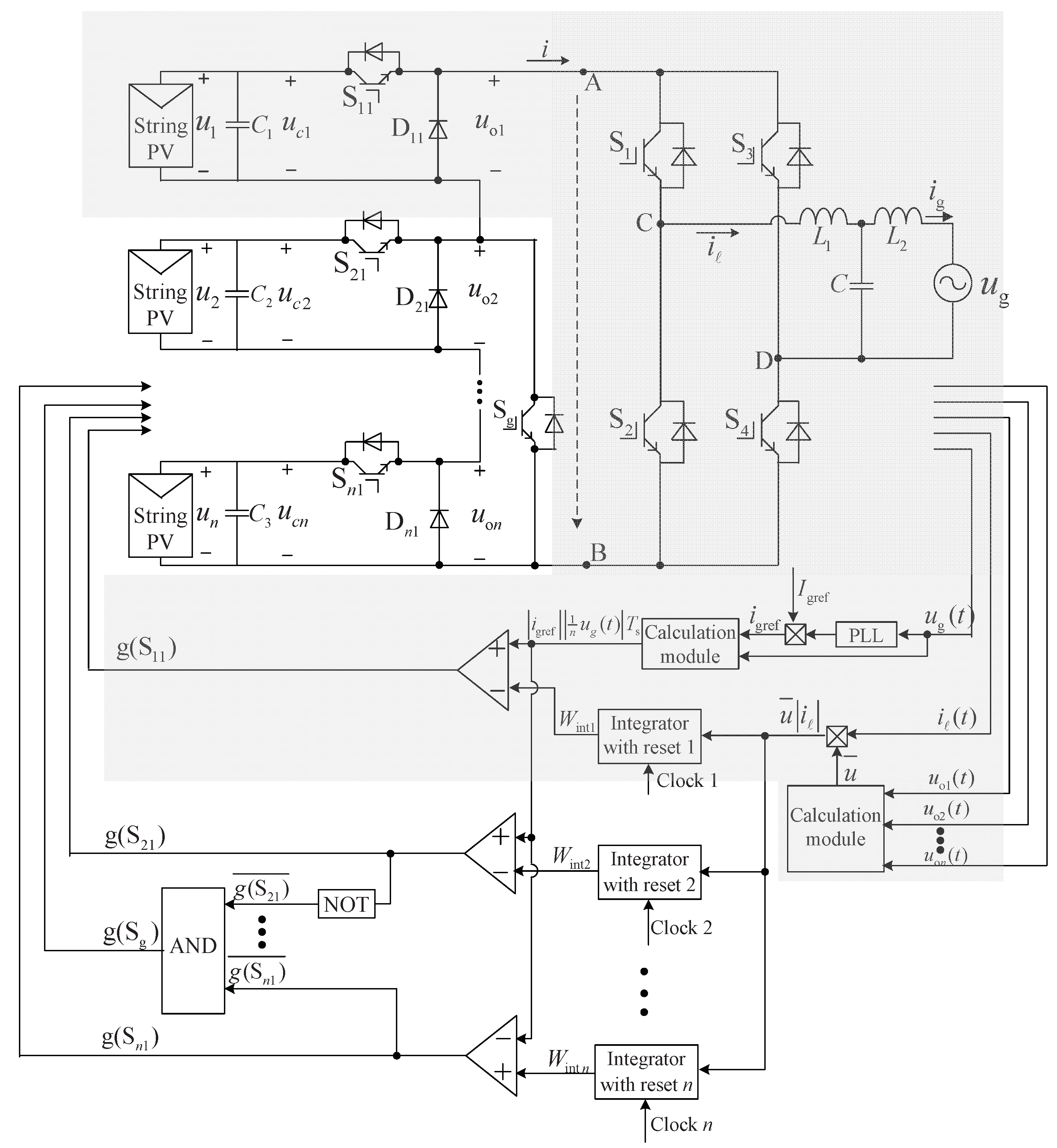
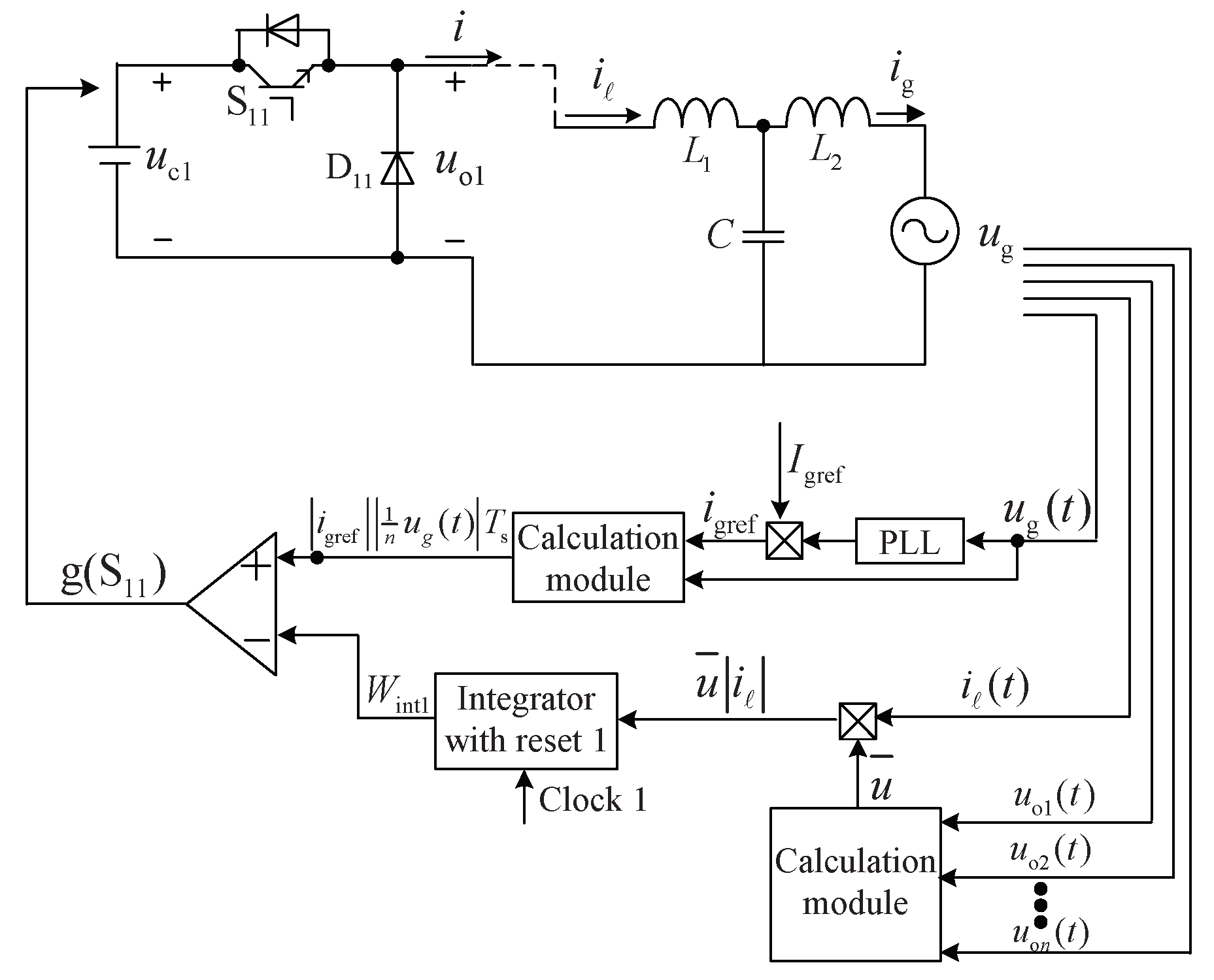
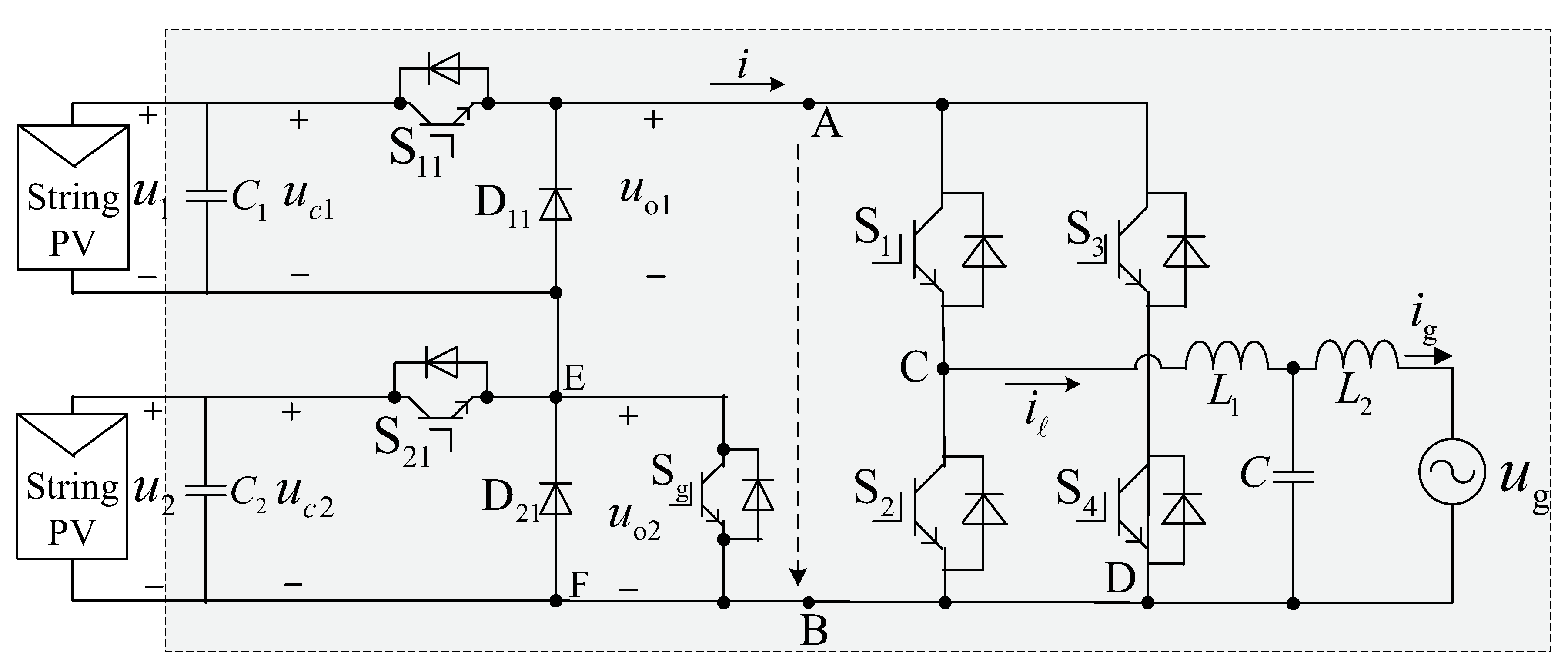
2. Deriving the Control Equation Based on the CSD Multilevel Topology

Figure 1 shows the block diagram of the PV CSD multilevel inverter with the proposed CPS energy balance control method. In Figure 1, the PV panels carry out the task of maximum power point tracking (MPPT). Because the goal of this research was to present a novel control method for the inverter, the MPPT stage was not implemented but emulated by DC sources with fluctuations, reflecting the low-harmonic voltage ripple.
As shown in Figure 1, the CSD topology comprises an n cascaded switched-diode converter, a spike removal switch S g and a full-bridge inverter, where n is the number of cascaded basic units. The basic unit 1 shown in Figure 1 consists of a PV string and a capacitor, which are emulated by a DC voltage source with fluctuations, a switch S 11 with its internal reverse diode and a diode D 11 . Then, u o 1 of the basic unit 1 will be one of two values, i.e., u c 1 when S 11 conducts and 0 when S 11 is turned off. The spike-removal switch S g provides a path for the reverse load current. It is connected between unit 2 and unit n and occurs when S 11 is on and the other switches are off.
Table 1 shows the switch states of the second stage. As shown in Table 1, the positive and negative halves of output waveforms are detected during the second stage of the multilevel inverter by comparing the reference current i gref with zero. Thus, the proposed CPS energy balance control method is designed for just the first stage, which only considers the positive state. The main principle of the proposed control method is to force the grid current to be equal to a desired value.
The following control equation is based on cascaded unit 1, as shown in Figure 2, which is the shaded part in Figure 1. For cascaded unit 1, the energy balance means that, during the n th switching cycle [ ( n 1 ) T s , n T s ) , where T s represents the switching cycle, the energy injected into the circuit is kept equal to the sum of the energy fed into the grid W g 1 ( n ) , the stored energy of L 1 and L 2 as Δ W ( n ) and that of the capacitor C as Δ W c ( n ) :
W in 1 ( n ) = W g 1 ( n ) + Δ W ( n ) + Δ W c ( n ) ( n = 1 , 2 , )
The circuit in Figure 2 can be seen as a buck converter, where u c 1 emulates the PV panels. As a buck converter, during the n th switching cycle, cascaded unit 1 operates in two states:
State 1: − S 11 is on for duration t on 1 ( n ) and, in this switching state, the energy is injected into the circuit and i flows through the loop ( u c 1 S 11 L 1 C L 2 and u g u c 1 ). L 1 and L 2 are charged, the grid is fed energy and u o 1 is derived using (2):
u o 1 ( t ) = u c 1 ( t [ ( n 1 ) T s , ( n 1 ) T s + t on 1 ( n ) )
State 2: − S 11 is off for duration t off 1 ( n ) and, in this switching state, no energy is fed into the circuit; however, i flows through the loop ( D 11 L C R D 11 ). L 1 and L 2 are discharged, the grid is fed energy and u o 1 is obtained using
u o 1 ( t ) = 0 ( t [ ( n 1 ) T s + t on 1 ( n ) , n T s )
According to the above state analysis, the values of W in 1 ( n ) , W grid 1 ( n ) during the nth switching cycle can be obtained as follows:
W in 1 ( n ) = ( n 1 ) T s ( n 1 ) T s + t on 1 ( n ) u o 1 ( t ) i ( t ) d t
substituting i = | i ( t ) | into (4) results in:
W in 1 ( n ) = ( n 1 ) T s ( n 1 ) T s + t on 1 ( n ) u c 1 ( t ) | i ( t ) | d t
W g 1 ( n ) = ( n 1 ) T s ( n 1 ) T s + T s | 1 n u g ( t ) | | i gref ( t ) | d t
Additionally, the purpose of this control mechanism is to ensure that the grid current i g ( n ) is equal to the reference grid current i gref ; thus, i g can be substituted by i gref , which is regarded as a constant value in a switching cycle. Then, u 2 can be calculated as follows:
u 2 = L d i g d t = L d i gref d t = 0
Then, u c is calculated as follows:
u c = u 2 + u g = u g
where u g is the grid voltage, which can also be regarded as a constant value in a switching cycle; thus, i c can be obtained in the following way:
i c = C d u c d t = C d u g d t = 0
Then, i 1 is calculated as follows:
i 1 = i c + i g = i g
From (10), it can be seen that i 1 is also regarded as a constant value since i g can be substituted by i gref as mentioned above. Then, u 1 can be obtained as follows:
u 1 = L d i 1 d t = 0
In a buck converter, the inductors work in the entire cycle during each switching cycle n; as a result, the stored energy of the inductor is calculated using (12):
Δ W ( t ) = Δ W 1 + Δ W 2 = ( n 1 ) T s ( n 1 ) T s + T s u 1 i 1 d t + ( n 1 ) T s ( n 1 ) T s + T s u 2 i 2 d t
By substituting (7) and (11) into (12), Δ W ( n ) can be derived as follows:
Δ W ( n ) = 0
Similarly, Δ W c ( n ) can be obtained as Δ W c ( n ) = 0 .
Thus, Δ W ( n ) and Δ W c ( n ) in (1) can be ignored and, combining the aforementioned state analysis, the energy conservation in the circuit can be realized by controlling u o 1 , which is expressed in (14):
( n 1 ) T s n T s u o 1 ( t ) | i ( t ) | d t = | u g | | i gref ( t ) | T s ( n = 1 , 2 , )

3. The Design and Implementation of the Proposed CPS Energy Balance Control Method

The control Equation (14) can be implemented using comparison and integration, as shown in Figure 2. The control implementation for cascaded unit 1 is described as follows: at the beginning of a switching cycle, when the pulse of clock 1 arrives, S 11 is turned on and the integrator starts working, whose value W int 1 ( k ) increases from its initial value. W int 1 ( t ) is compared with the control reference W g 1 instantaneously. At the instant when W int 1 ( t ) reaches W g 1 , the output of the comparator changes to a low level, which turns off S 11 . Then, S 11 is switched from the on state to the off state. S 11 is switched off until the arrival of the next clock pulse, which resets the integrator and starts the ( n + 1 ) th switching cycle.
As shown in Figure 1, u o 1 can be replaced by u ¯ , which is the average value of all the values of the DC link ( u c 1 , · · · , u c 1 , u cn ); then, (14) can be rewritten as follows:
( n 1 ) T s n T s u ¯ ( t ) | i ( t ) | d t = | u g | | i gref ( t ) | T s ( n = 1 , 2 , )
Thus, the input value of all the reset integrators can be obtained using (15). Additionally, the controls of the other cascaded units are similar to that of cascaded unit 1, but with a phase-shift for T s / n of the clock pulse. Furthermore, the spike removal switch S g , which is connected between unit 2 and unit n, is controlled by operations when S 11 is on and S 21 to S n 1 is off.

4. Simulation Results

In order to verify the feasibility and performances of the proposed control method, a 5-level and a 17-level CSD topology were developed using MATLAB/Simulink. During the simulation, the MPPT stage was not implemented but simulated by DC sources with fluctuations. A comparative study using a conventional PS-PWM control method is presented to evaluate the performances of the proposed method. The PS-PWM grid-connected system was designed using the SISO tool of MATLAB with phase and amplitude margins of 32.7 and 7.61 dB, respectively.

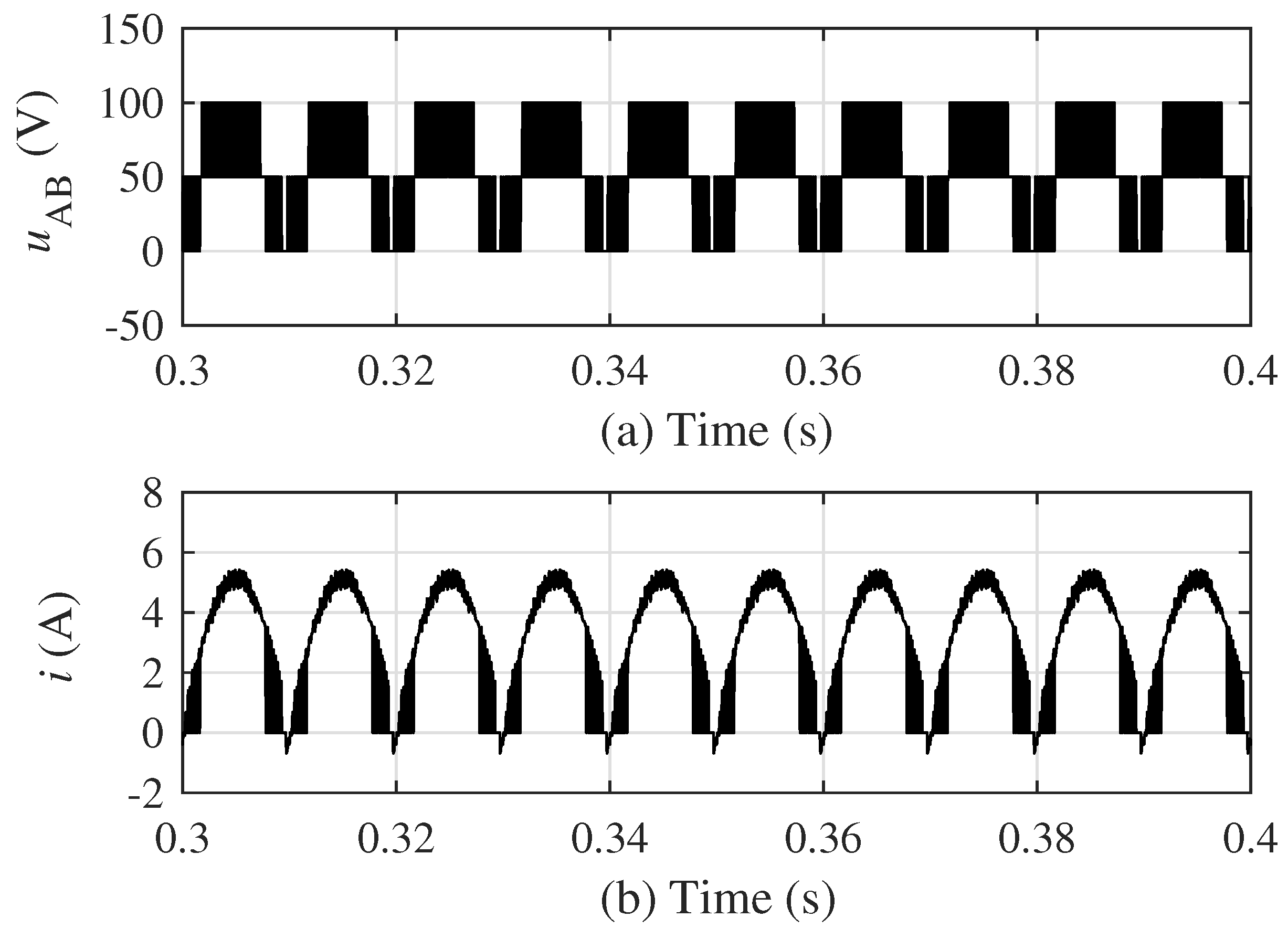
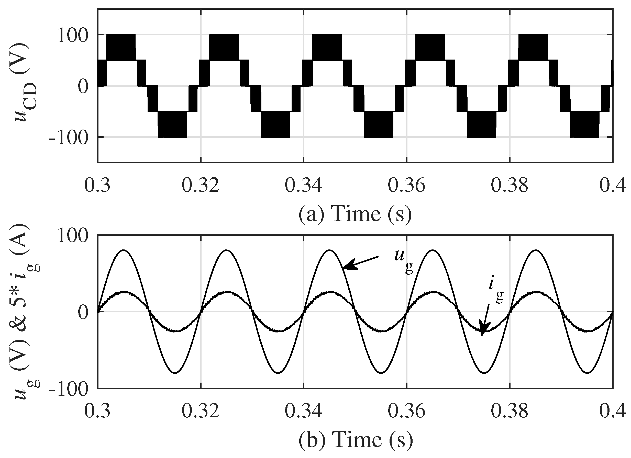
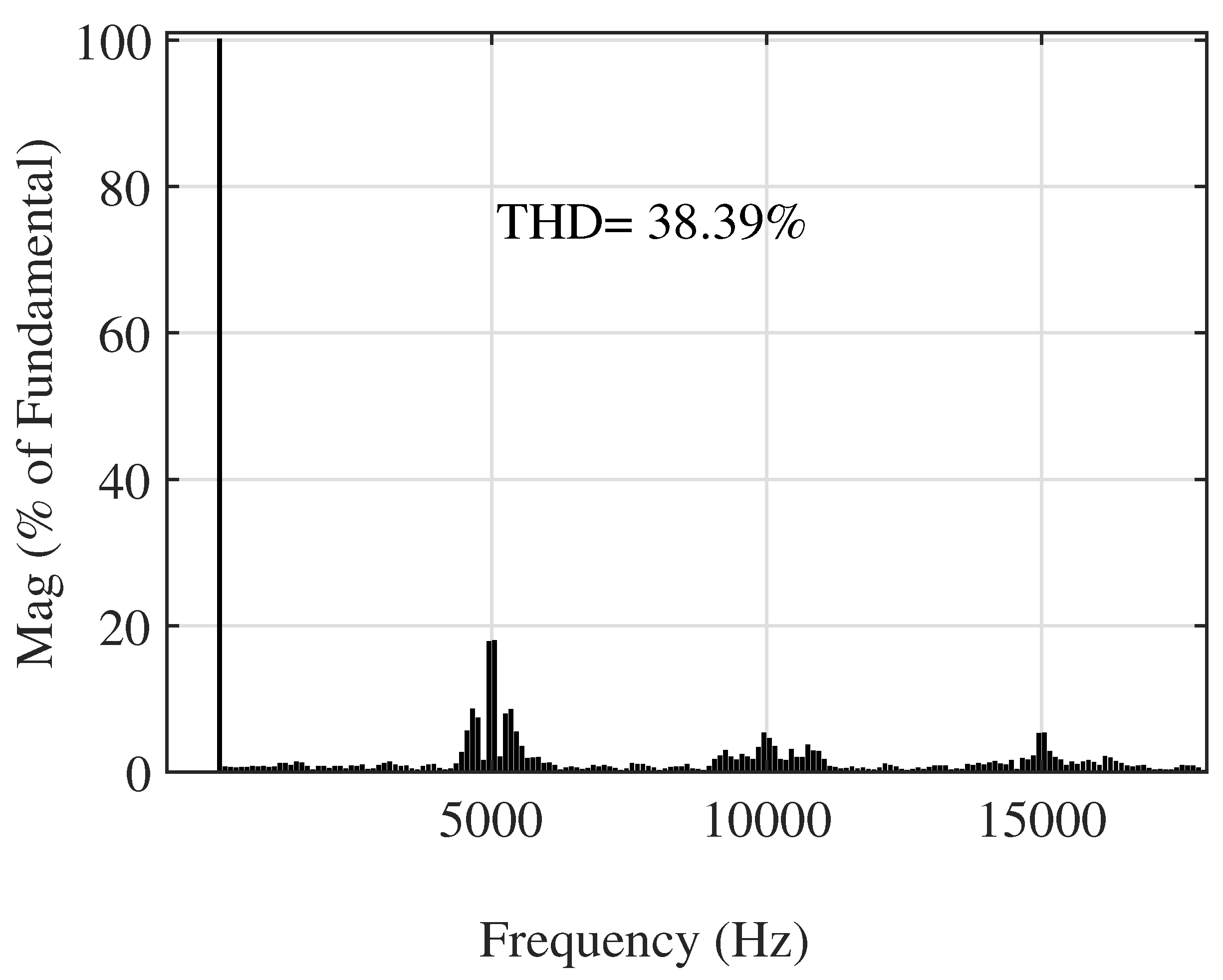
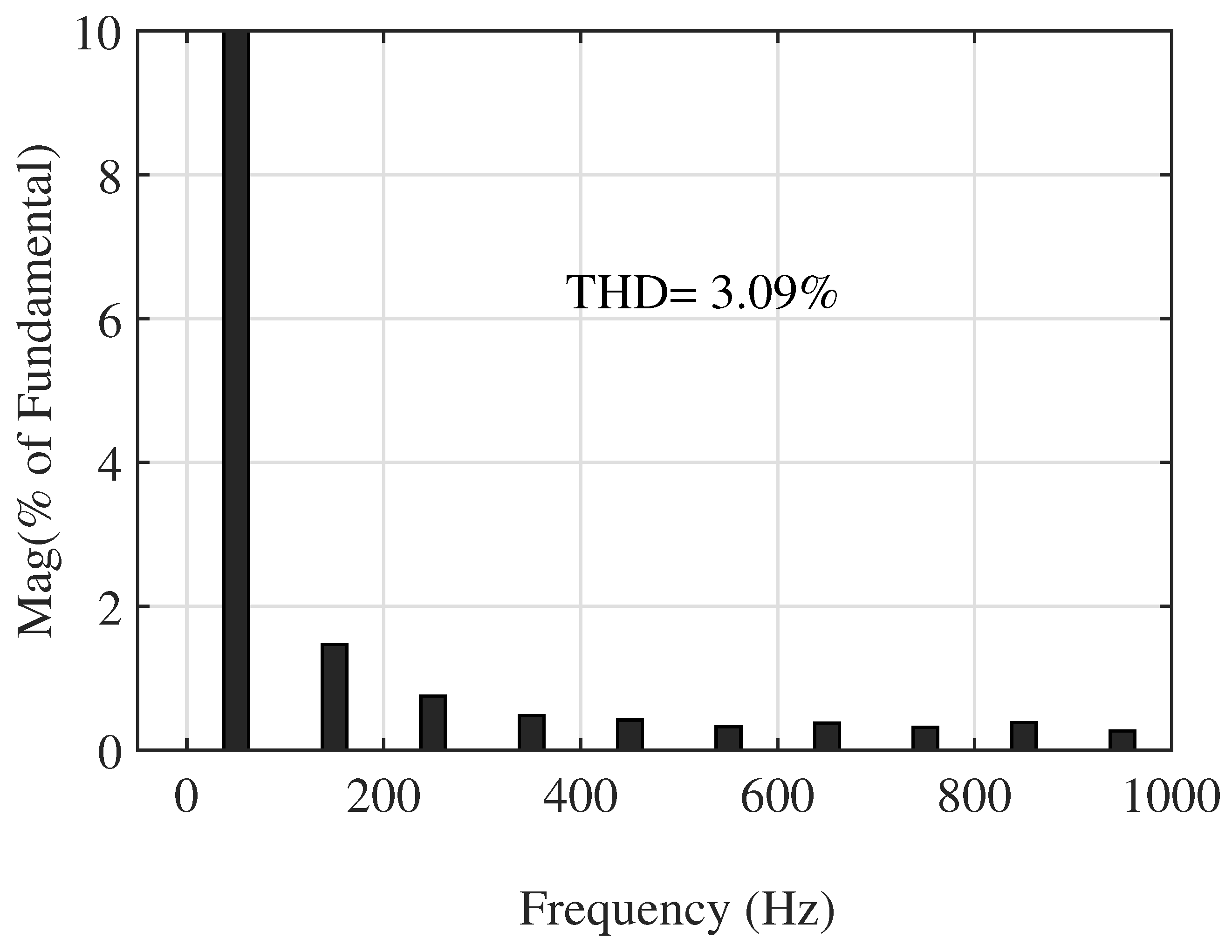
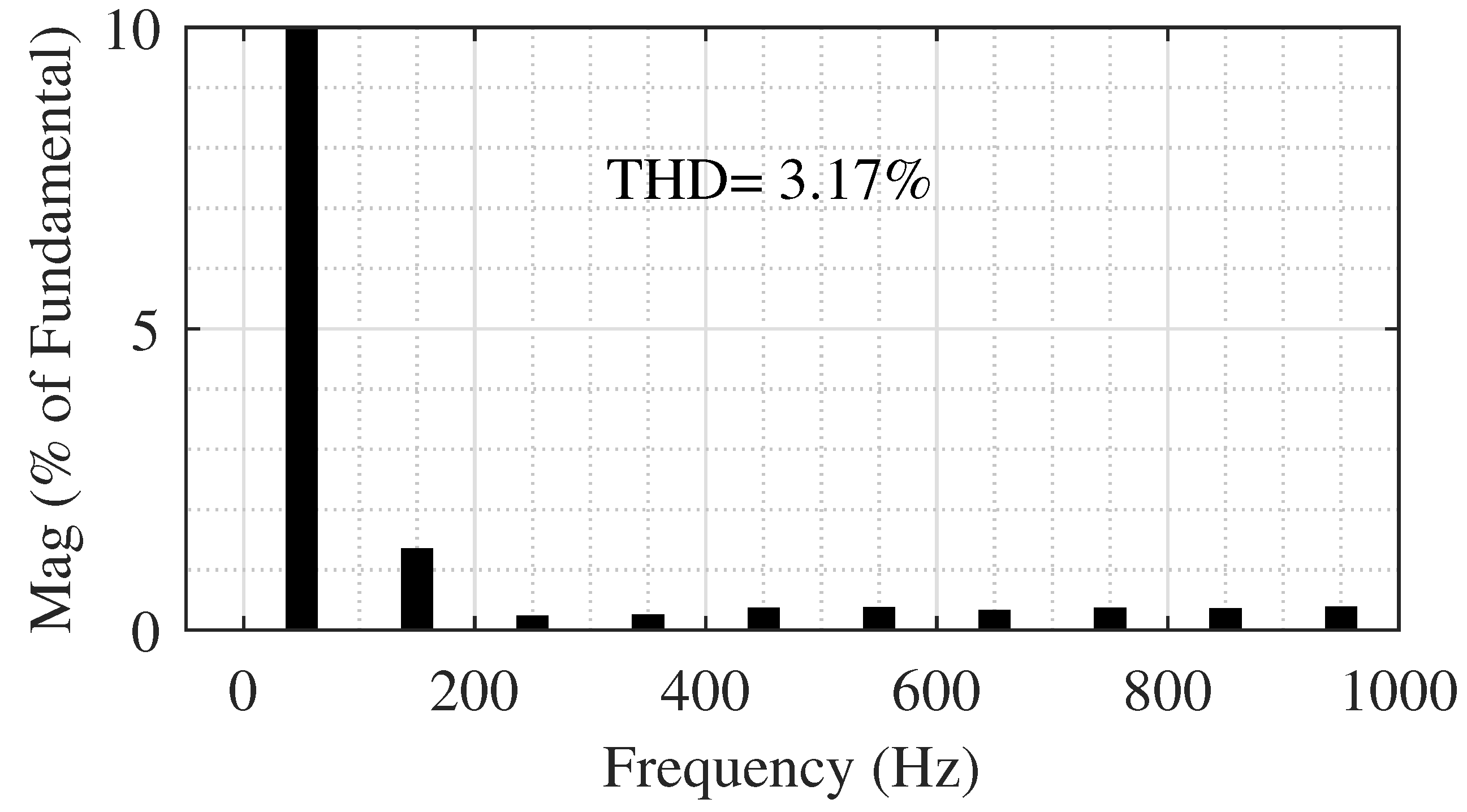
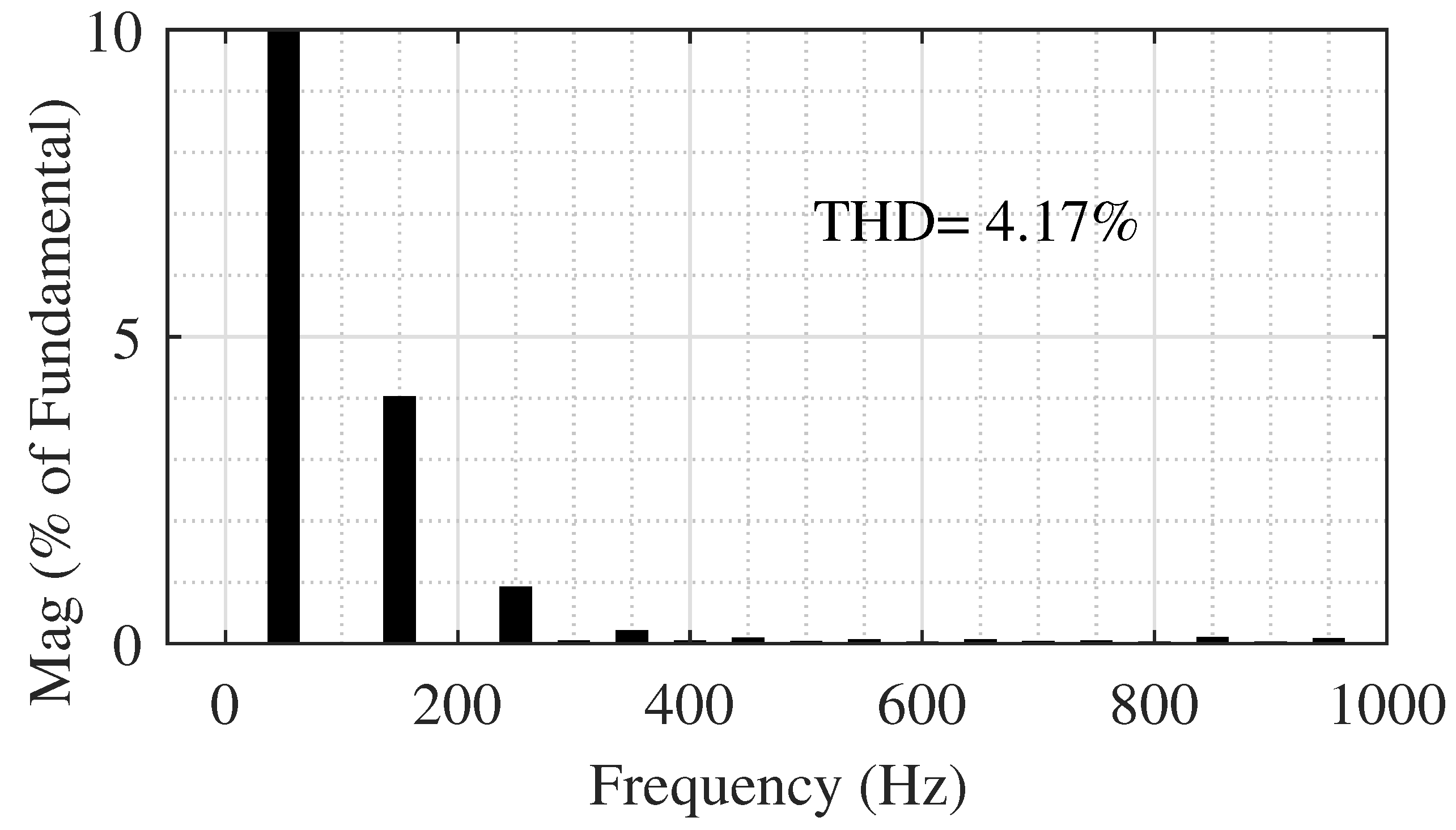
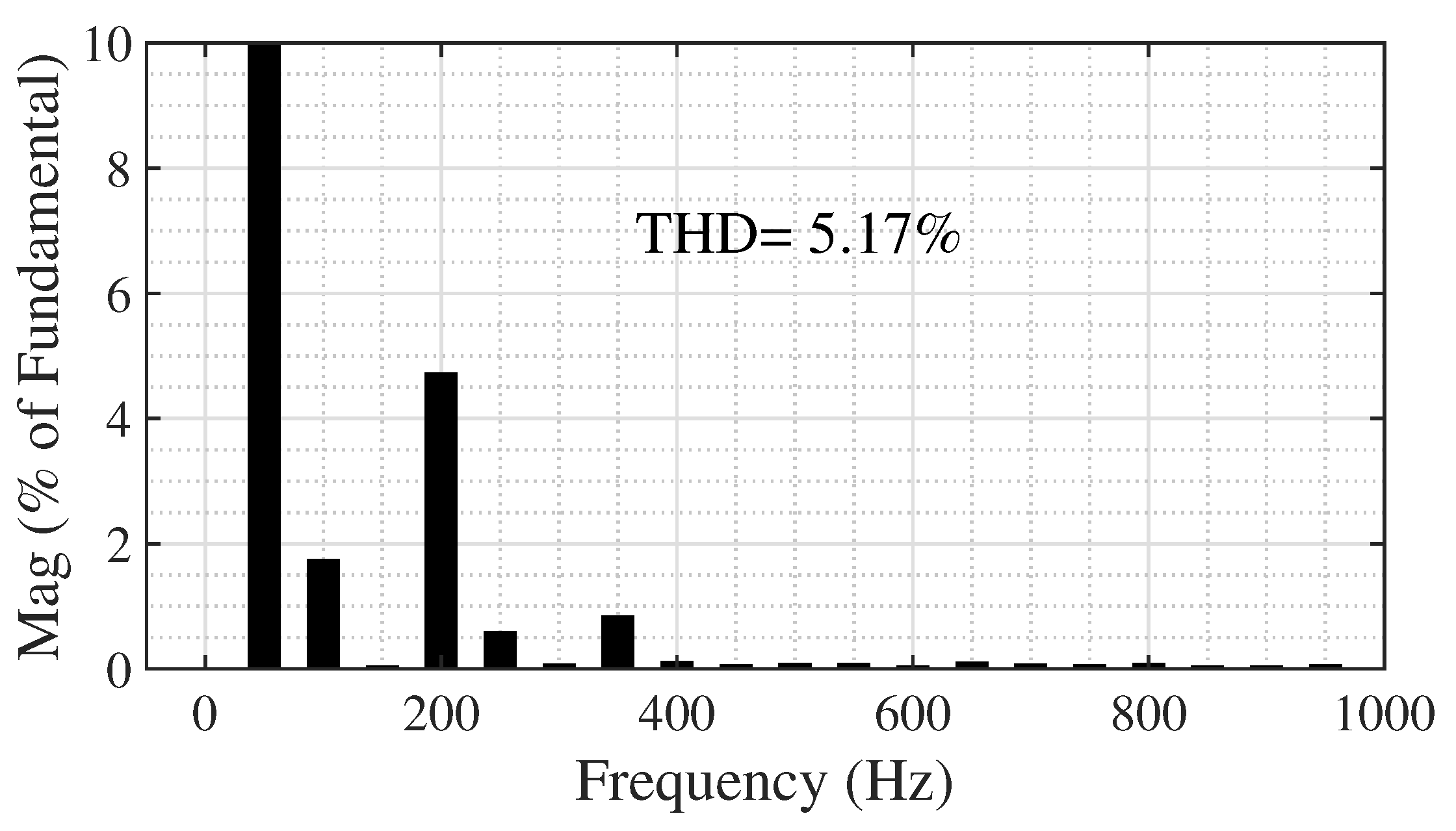
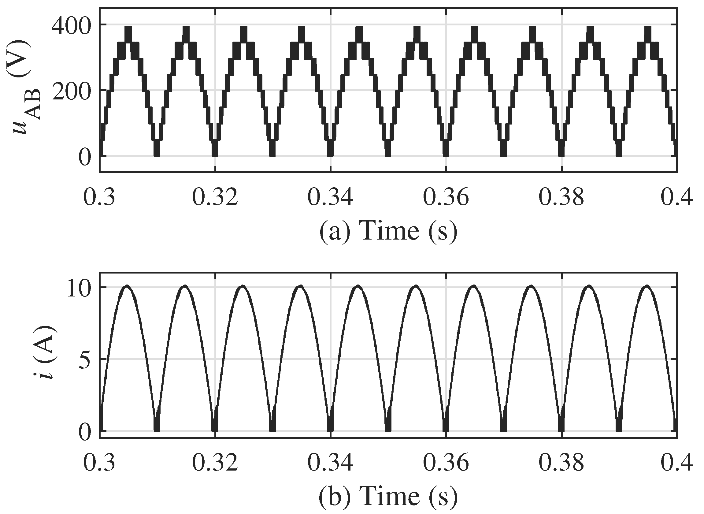
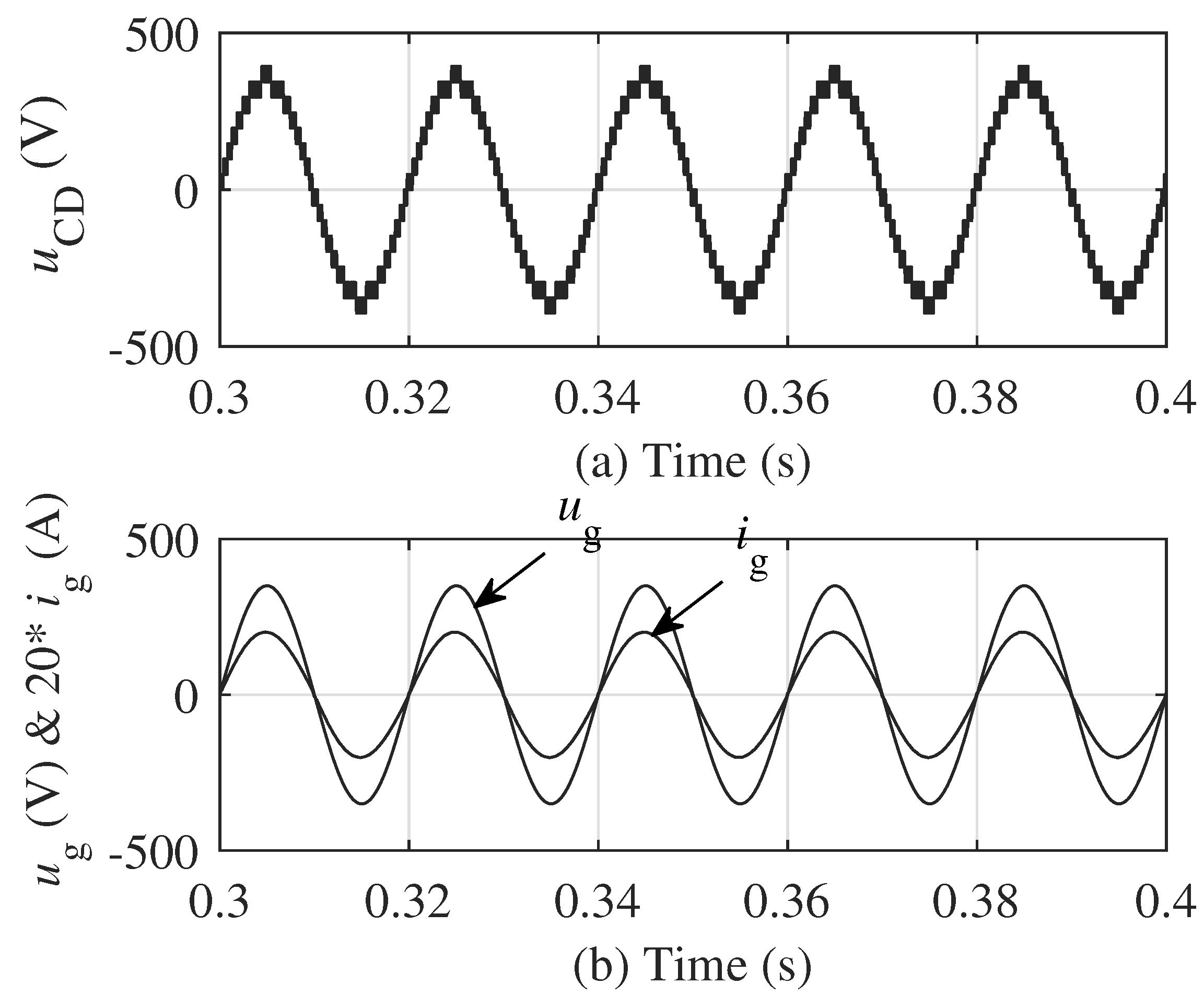
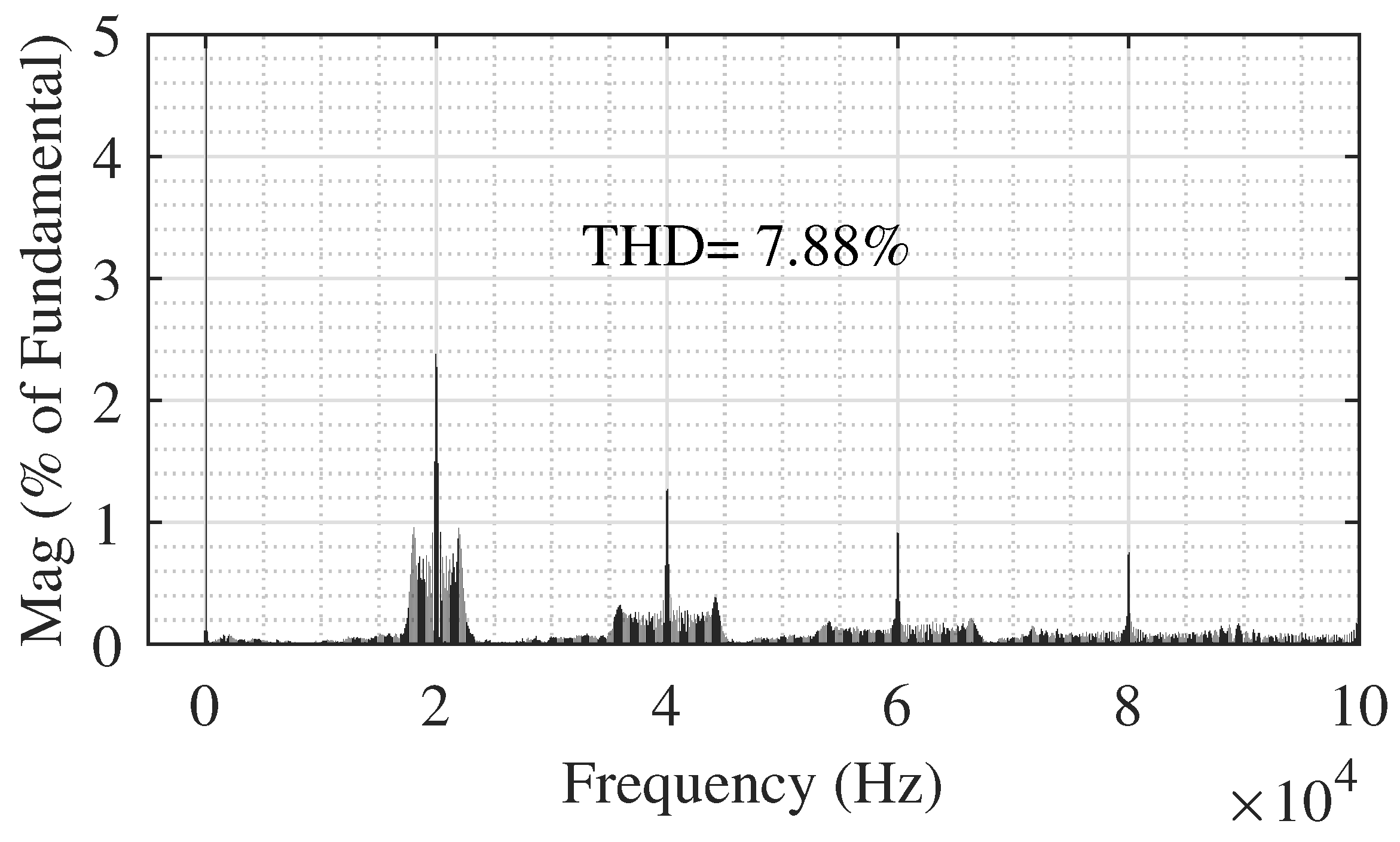
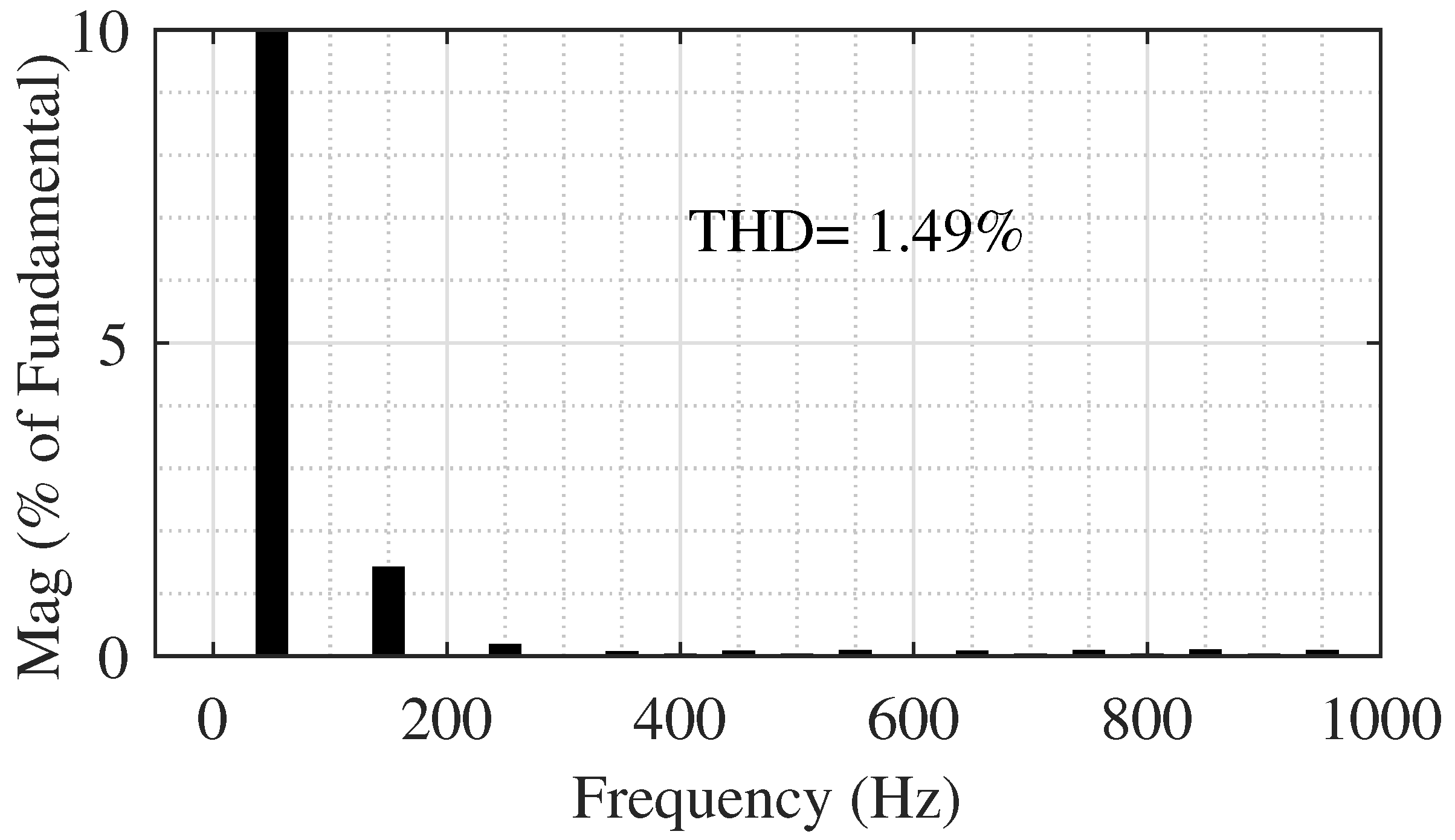
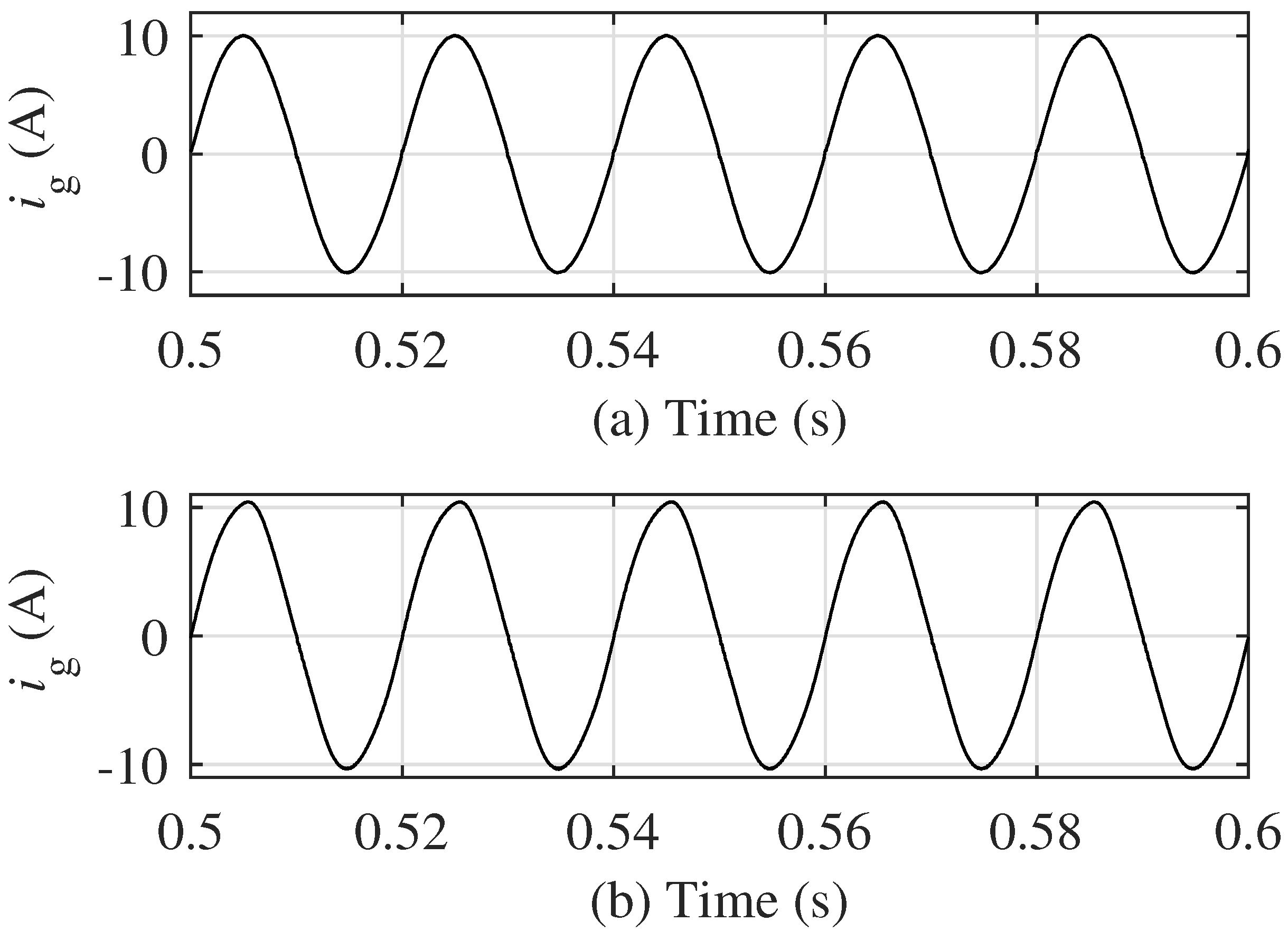
4.1. Simulation Results of the 5-Level Topology

The diagram of a 5-level CSD topology is shown in Figure 3. It comprises a two-cascaded switched-diode converter, a spike removal switch S g and a full-bridge inverter. The spike removal switch S g is connected between E and F and operates when S 11 is on and S 21 is off. The circuit parameters are listed in Table 2.
Figure 4 and Figure 5 show the simulation results of the operation of the PV cascaded multilevel grid-connected inverter with the proposed control method. From Figure 4, it can be observed that, as the sum of the output value of all the cascaded units, u AB and the current i of the first-stage have zero and positive values. Figure 5 shows the waveform of u CD , which is a 5-level stepped waveform. The waveform of i g in Figure 5 illustrates that, after the L C L filter, it is sinusoidal and in phase with the grid voltage.
The THD of the stepped output voltage waveform u CD of the 5-level multilevel inverter is 38.39%, as shown in Figure 6. The frequencies of the main harmonics are twice the switching frequency ( 2500 Hz ) and its multiples. After the L C L filter, the THD of i g is 3.09%, as shown in Figure 7. Additionally, the calculation result of the power factor is 99.98%, which means that the power factor is almost unity.
From these results, it is clear that the proposed CPS energy balance control method is feasible for the CSD multilevel inverter for the grid-connected PV system.
Figure 8 show the 5-level simulation results of the suppression ability against second-order harmonics in a DC link, which is realized by adding second-frequency harmonic ripples into the DC link voltages of each cascaded unit. Figure 8 illustrates the results under the case where the DC link is added with a second-harmonic voltage ripple, which has an amplitude of 8 V . Although the distortion caused by this harmonic is not obvious from the waveform, the FFT analysis of Figure 9 and Figure 10 illustrate that i g using PS-PWM contains corresponding harmonics to those of the DC link voltage, whose THD has increased to 4.17%. In contrast, the THD of i g using the proposed control method is 3.17%, with a slight increase.
Although the harmonics that the PV system may contain are mainly the second-harmonic voltage ripples, other low-frequency harmonics may also be caused by environmental factors; for example, the irradiance level varies in a certain range. Thus, third-harmonic voltage ripples with an amplitude of 8 V are added in DC links of the 5-level topology. The simulation results are shown in Figure 11. From the waveform in Figure 11a, it can be seen that, using the proposed control method, i g remains a consistent output, and the FFT analysis of Figure 12 illustrates that the THD is 3.18%, with a slight increase. In contrast, the waveform when using the PS-PWM control method is distorted obviously, as shown in Figure 11b. Additionally, from the FFT analysis of Figure 13, it can be observed that the corresponding harmonics propagate from the DC link to the power grid, leading the THD to increase to 5.17%.

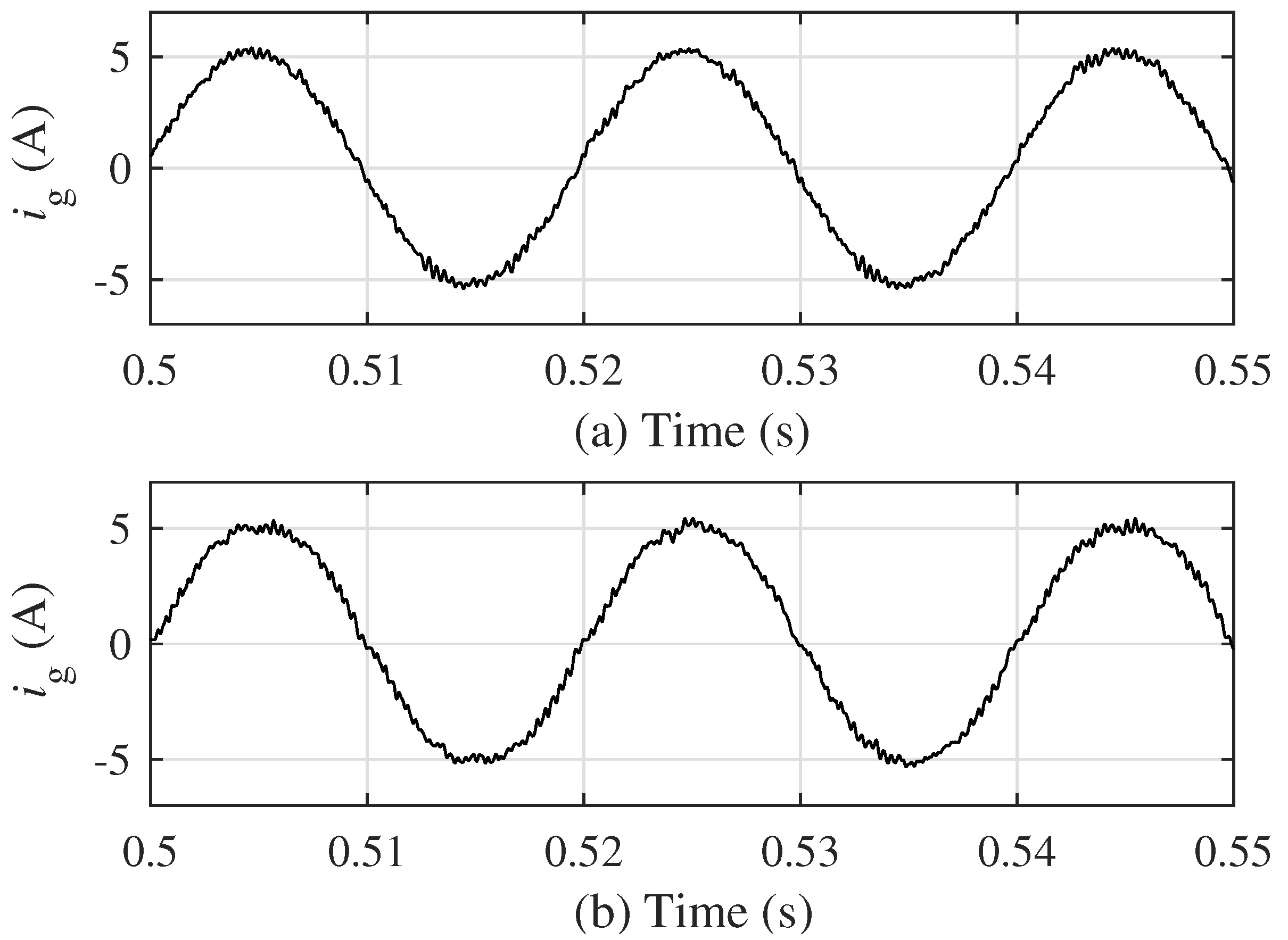
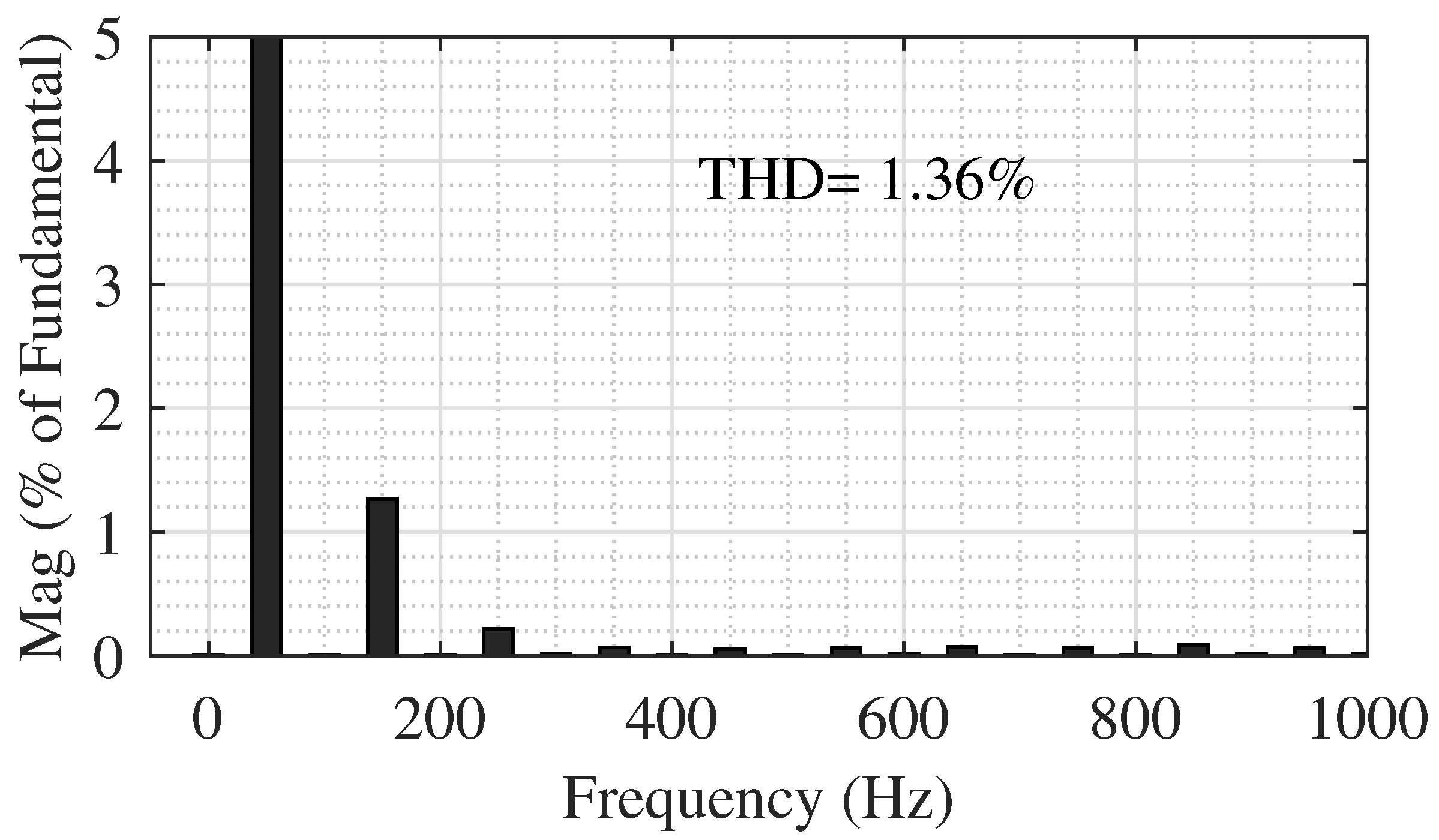
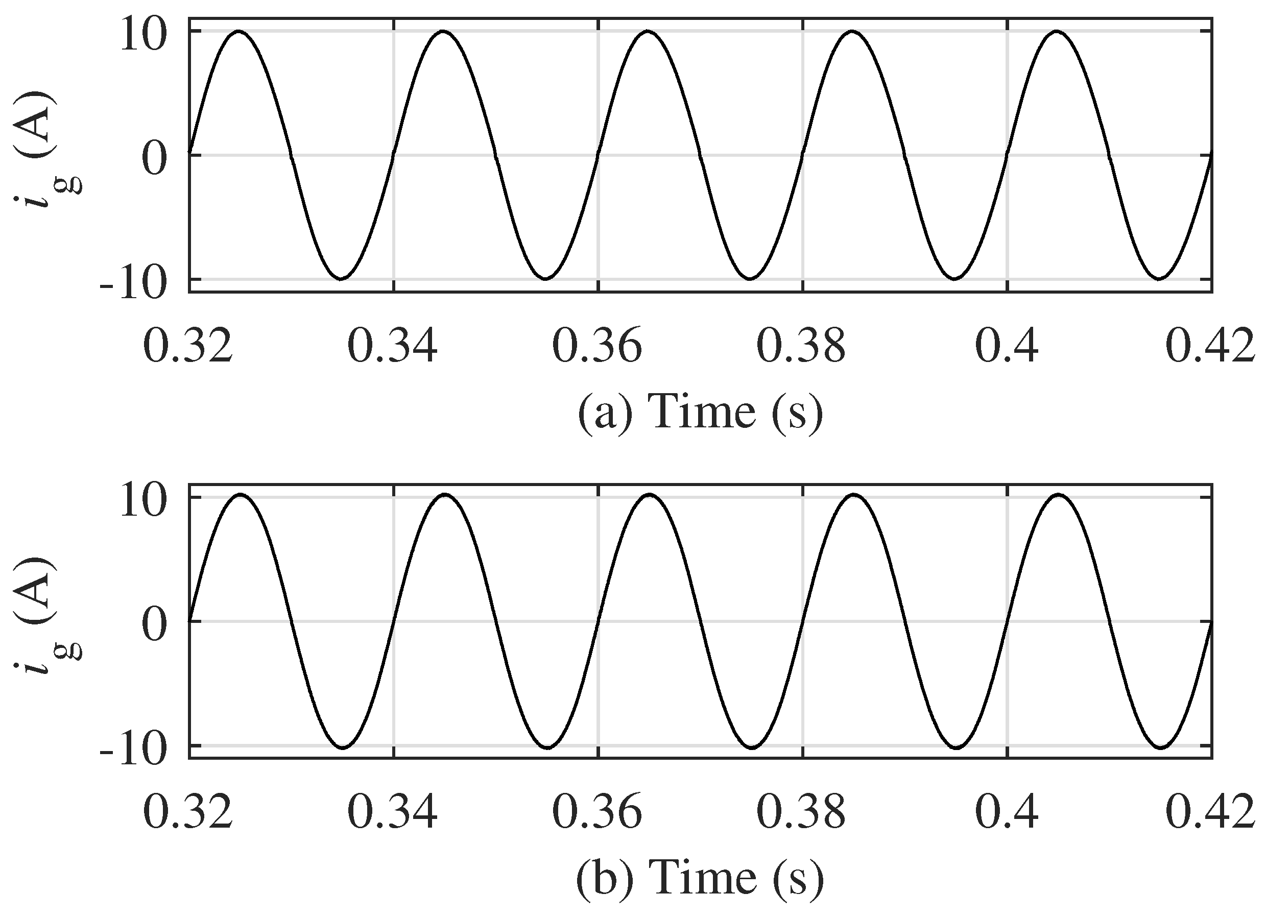
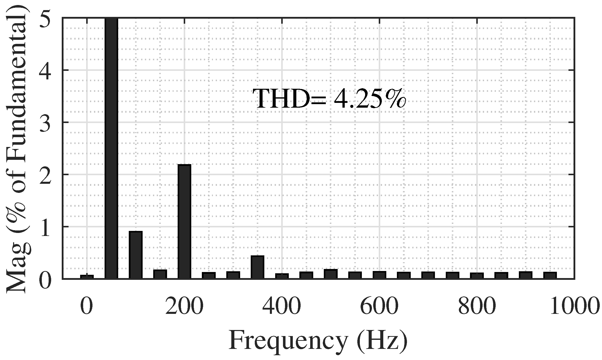
4.2. Simulation Results of the 17-Level Topology

The 17-level CSD topology is similar to that of the 5-level topology shown in Figure 3. However, it comprises an eight-cascaded switched-diode converter, a spike removal switch S g and a full-bridge inverter. The spike removal switch S g is connected between unit 2 and 8 and works when S 11 is on and all the other switches are off. The circuit parameters are listed in Table 3.
Figure 14 and Figure 15 show the simulation results of the operation of the 17-level CSD cascaded multilevel grid-connected inverter with the proposed control method. From Figure 14, it can be observed that, as the sum of the output value of all the cascaded units, u AB and the current i of the first stage has zero and positive values. Additionally, Figure 15 shows the waveform of u CD , which is a 17-level stepped waveform. The waveform of i g in Figure 15 illustrates that, after the L C L filter, it is sinusoidal and in phase with the grid voltage.
The THD of the stepped output voltage waveform u CD of the 17-level multilevel inverter is 7.88%, as shown in Figure 16. The frequencies of the main harmonics are eight times the switching frequency ( 2500 Hz ) and its multiples. Compared with the THD of u CD of the 5-level multilevel inverter, the THD is lower and the frequencies that the main harmonics focus on move backward. Figure 17 shows the THD of i g , which is 1.36%. Additionally, the calculation result of the power factor is 99.982%, which means that the power factor is close to unity.
From these results, it is clear that the proposed CPS energy balance control method is feasible for the CSD multilevel inverter for the grid-connected PV system.
Figure 18 illustrates the results of the case where the DC link is added with a second-harmonic voltage ripple, which has an amplitude of 8 V . Although the distortion caused by this harmonic is not obvious, as shown in the waveforms, the FFT analysis of Figure 19 and Figure 20 illustrates that i g using PS-PWM contains corresponding harmonics to those of the DC link voltage, for which the THD increased to 2.92%. In contrast, the THD of i g using the proposed control method is 1.49%, with a slight increase.
Figure 21 illustrates the results of the case where the DC link is added with a third-harmonic voltage ripple, which has an amplitude of 8 V . From the waveform in Figure 21a, it can be seen that, using the proposed control method, i g is a consistent output, and the FFT analysis of Figure 22 illustrates that the THD is 1.41%, with a slight increase. In contrast, the waveform when using the PS-PWM control method is distorted clearly, as shown in Figure 21b. Additionally, from the FFT analysis of Figure 23, it can be observed that corresponding harmonics propagate from the DC link to the power grid, leading to the THD increasing to 4.25%.

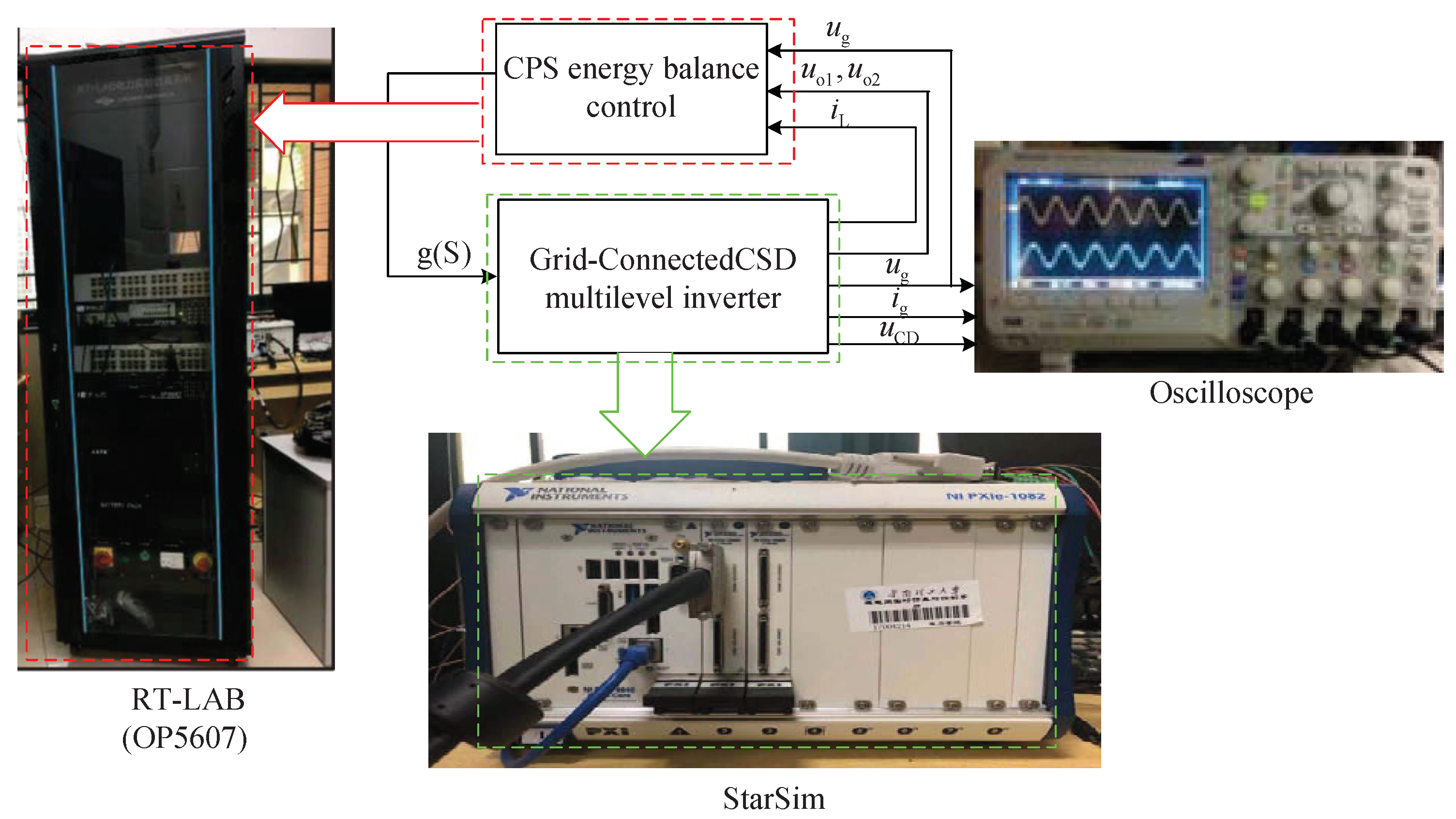
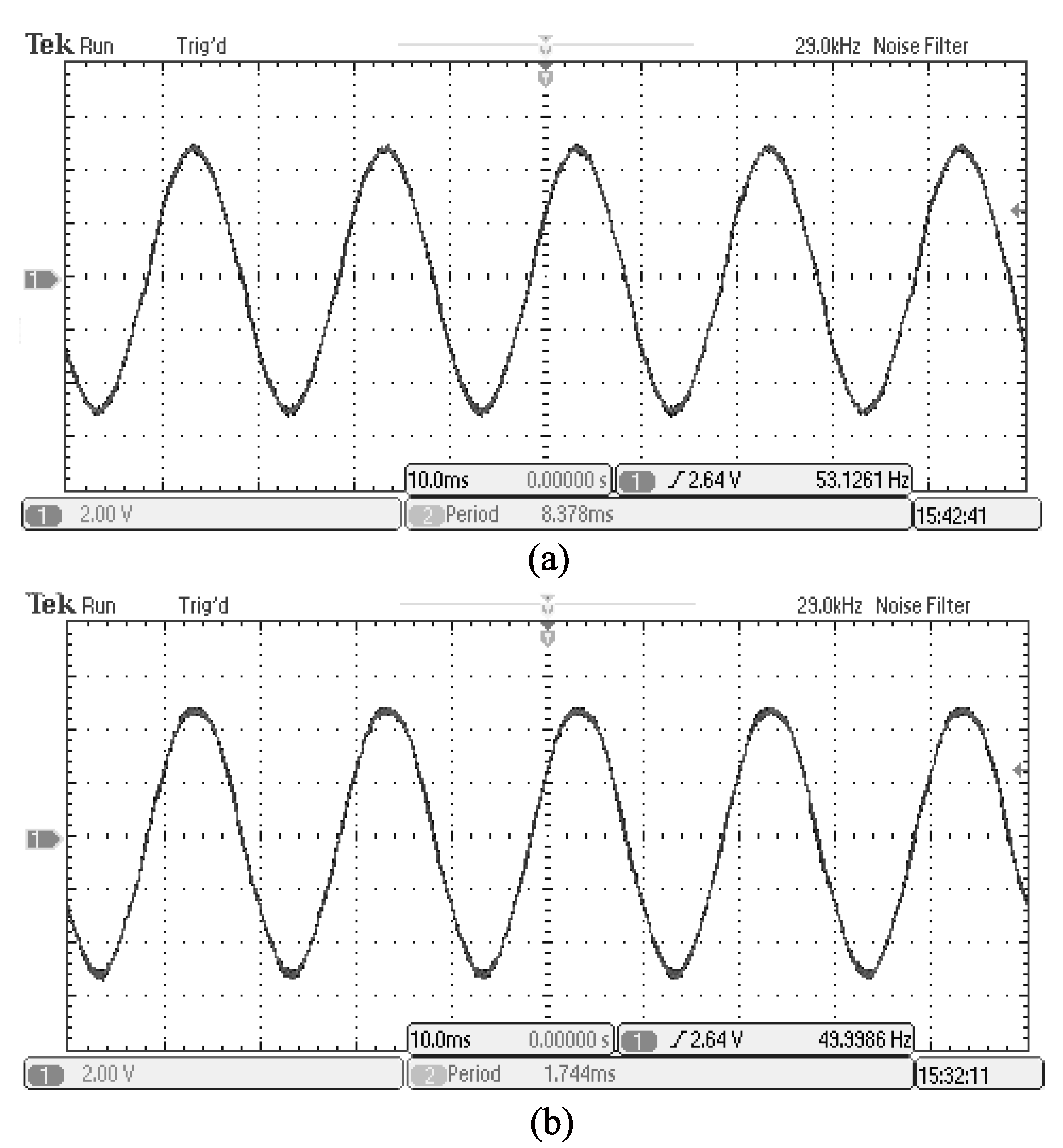
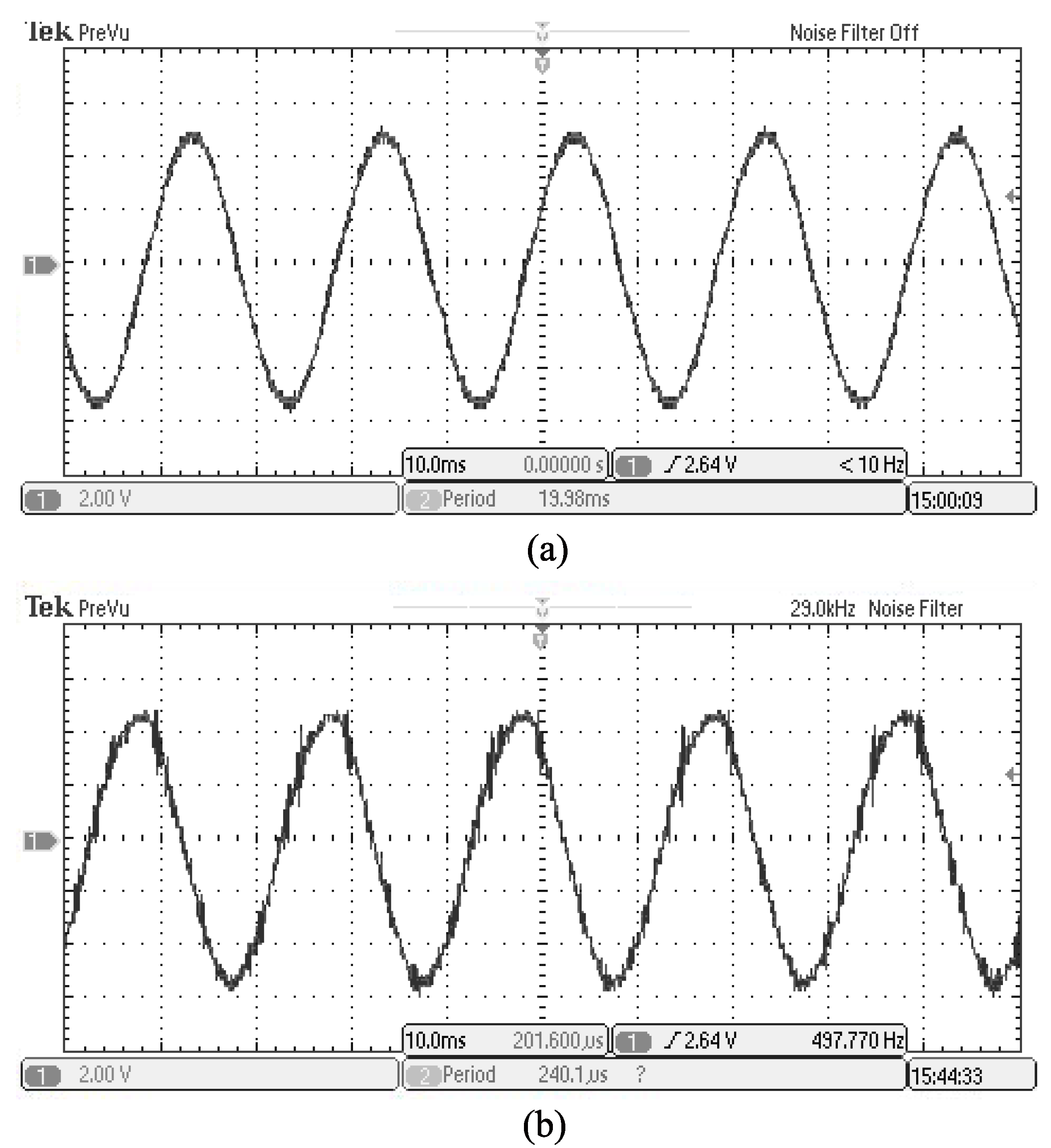
5. Experimental Verification

According to the parameters listed in Table 2, a 5-level experimental prototype was built, as shown in Figure 24. In the experiment, a real-time implementation of the hardware-in-the-loop (HIL) system was used to verify the proposed CPS energy balance control method. The model of a 5-level CSD topology was developed in the electromagnetic transient simulation software StarSim, and ran on a PXI-FPGA-based real time HIL system with a time step of 1 × 10 3 . The HIL testing system parameters were the same as the ones in the simulation tests. The control methods were implemented using the RTlab 5600 platform. The sampling period of the controller and the switching frequency were selected as 20 μ s and 2.5 kHz , respectively. The connection of the HIL simulation system and RTlab 5600 was implemented by using many IO channels. The oscilloscope measured the output voltage and grid current of the 5-level CSD topology.
Figure 25 shows the experimental results of the 5-level topology using the proposed control method. The stepped voltage, grid voltage and current are depicted. It can be observed that the experimental results are consistent with the simulation results in Figure 5. A 5-level staircase waveform was implemented, the grid current was sinusoidal and synchronization took place with the grid voltage. The results of the FFT analysis illustrate that the THD is 40.47% of u CD and 4.09% of i g . The power factor is calculated as 98.28%.
Figure 26 and Figure 27 show the comparison results of the prevention of low-frequency ripples of the DC link propagating to the power grid. From the results, it can be demonstrated that the experimental results are consistent with the simulation results shown in Figure 26 and Figure 27, meaning that i g using PS-PWM contains corresponding harmonics from the fluctuations in the DC link. In contrast, when using the proposed control method, there are almost no new harmonics propagated to i g . These results illustrate that the proposed control method has a superior ability and can prevent the low-frequency ripple of the DC link propagating to the power grid.

6. Conclusions

Based on the energy balance principle in the circuit, a CPS energy balance control method was proposed for PV-cascaded multilevel grid-connected inverters in this paper. At first, the control principle is introduced and the control equation was analyzed and derived. By shifting the phase of the clock pulse of each cascaded unit, the control method was implemented using a comparator and integrator. The analysis and results illustrate that it has a simple structure and is simple to implement. Taking the 5-level and 17-level prototypes as examples, the feasibility and performance of the method were tested and verified by performing simulations and experiments. The results reveal that the proposed CPS energy balance control method can obtain staircase-like voltage waveforms and a grid sinusoidal input current with a low harmonic distortion. Moreover, compared to the PS-PWM method, the proposed CPS energy balance control method has a superior ability in the prevention of low-frequency ripples of the DC link propagating to the power grid. These results provide new insights for the control of multilevel inverters of grid-connected PV applications. In this study, we assessed the proposed CPS energy balance control method’s ability to prevent low-frequency ripples in the DC link; in the future, its ability to alleviate the inter-bridge power imbalance and tracking ability of the reference current will be studied.

Author Contributions

Conceptualization, L.W. and W.M.; methodology, L.W.; software, L.W.; validation, L.W. and L.C.; writing—original draft preparation, L.W.; writing—review and editing, W.M.; supervision, W.Y. All authors have read and agreed to the published version of the manuscript.

Funding

This research was funded by the National Natural Science Foundation of China (Grant No. 62001169).

Conflicts of Interest

The authors declare no conflict of interest.

Abbreviations

The following abbreviations are used in this manuscript:
CPSclock phase-shifted
PVphotovoltaic
DGdistributed generation
CSDcascaded switched-diode
THDtotal harmonic distortion
PS-PWMphase-shifted pulse width modulation
MPPTmaximum power point tracking

References

  1. Wang, T.; O’Neill, D.; Kamath, H. Dynamic control and optimization of distributed energy resources in a microgrid. IEEE Trans. Smart Grid 2015, 6, 2884–2894. [Google Scholar] [CrossRef] [Green Version]
  2. Hussain, M.M.; Javed, W.; Akram, R.; Javed, T.; Razaq, A.; Siddique, M. Distributed energy management analysis for microgrids. In Proceedings of the 2021 56th International Universities Power Engineering Conference (UPEC), Middlesbrough, UK, 31 August–3 September 2021; pp. 1–6. [Google Scholar]
  3. Xiao, B.; Hang, L.; Mei, J.; Riley, C.; Tolbert, L.M.; Ozpineci, B. Modular cascaded H-bridge multilevel PV inverter with distributed MPPT for grid-connected applications. IEEE Trans. Ind. Appl. 2015, 51, 1722–1731. [Google Scholar] [CrossRef]
  4. Mittal, N.; Singh, B.; Singh, S.P.; Dixit, R.; Kumar, D. Multilevel inverters: A literature survey on topologies and control strategies. In Proceedings of the 2012 2nd International Conference on Power, Control and Embedded Systems, Allahabad, India, 17–19 December 2012; pp. 1–11. [Google Scholar]
  5. Wang, L.; Wu, Q.H.; Tang, W.H. Novel cascaded switched- diode multilevel inverter for renewable energy integration. IEEE Trans. Energy Convers. 2017, 32, 1574–1582. [Google Scholar] [CrossRef]
  6. Alishah, D.N.R.S.; Hosseini, S.H. Novel topologies for symmet- ric, asymmetric, and cascade switched-diode mutilevel converter with minimum number of power electronic components. IEEE Trans. Ind. Electron. 2014, 61, 5300–5310. [Google Scholar] [CrossRef]
  7. Babaei, E.; Hosseini, S.H. New cascaded multilevel inverter topology with minimum of switches. Energy Convers. Manag. 2009, 50, 2761–2767. [Google Scholar] [CrossRef]
  8. Alishah, R.S.; Nazarpour, D. New hybrid structure for multilevel inverter with fewer number of components for high-voltage levels. IET Power Electron. 2013, 7, 96–104. [Google Scholar] [CrossRef]
  9. Devi, V.S.K.; Srivani, S.G. Modified phase shifted PWM for cascaded H bridge multilevel inverter. In Proceedings of the 2017 Third International Conference on Advances in Electrical, Electronics, Information, Communication and Bio-Informatics (AEEICB), Chennai, India, 27–28 February 2014; Volume 29, pp. 347–355. [Google Scholar]
  10. Garg, V.; Sinha, S.K.; Dave, M.P. Phase shifted PWM cascaded multilevel inverter for solar PV grid integration. In Proceedings of the 2016 IEEE 1st International Conference on Power Electronics, Intelligent Control and Energy Systems (ICPEICES), Delhi, India, 4–6 July 2016; pp. 1–5. [Google Scholar]
  11. Schenck, M.E.; Lai, J.S.; Stanton, K. Fuel cell and power conditioning system interactions. In Proceedings of the Twentieth Annual IEEE Applied Power Electronics Conference and Exposition, Austin, TX, USA, 6–10 March 2005; pp. 114–120. [Google Scholar]
  12. Michail, V.; Alfred, R.; Antoine, B. Modular converter architecture for medium voltage ultra fast ev charging stations: Global system considerations. In Proceedings of the IEEE International Electric Vehicle Conference (IEVC), Greenville, SC, USA, 4–8 March 2012; pp. 1–7. [Google Scholar]
  13. Cai, W.; Liu, B.; Duan, S.; Jiang, L. An active low-frequency ripple control method based on virtual capacitor concept for BIPV sytems. IEEE Trans. Power Electron. 2014, 29, 1733–1745. [Google Scholar] [CrossRef]
  14. JItoh, I.; Hayashi, F. Ripple current reduction of a fuel cell for a single-phase isolated converter using a DC active filter with a center tap. IEEE Trans. Power Electron. 2010, 25, 550–556. [Google Scholar]
  15. Shi, Y.J.; Liu, B.Y.; Duan, S.X. Low-frequency input current ripple reduction based on load current feedforward in a two-stage single-phase inverter. IEEE Trans. Power Electron. 2016, 31, 7972–7985. [Google Scholar] [CrossRef]
  16. Zhu, G.; Ruan, X.; Zhang, L.; Wang, X. On the reduction of second harmonic current and improvement of dynamic response for two stage single-phase inverter. IEEE Trans. Power Electron. 2015, 30, 1028–1041. [Google Scholar] [CrossRef]
  17. He, L.; Zhang, K.; Xiong, J.; Fan, S.; Xue, Y. Low-Frequency Ripple 48 Suppression for Medium-Voltage Drives Using Modular Multilevel Converter with Full-Bridge Submodules. IEEE J. Emerg. Sel. Top. Power Electron. 2016, 4, 657–667. [Google Scholar] [CrossRef]
  18. Wang, L.; Zhang, L.; Xiong, Y.; Ma, R. Low-frequency suppression strategy based on predictive control model for modular multilevel converters. J. Power Electron. 2021, 21, 1407–1415. [Google Scholar] [CrossRef]
  19. Wang, K.; Kong, D.; Zhong, Z.; Gao, N.; Jiang, F.; Wu, W.; Liserre, M. Suppression of Low-frequency Voltage Ripple in 56 Cascaded H-bridge Multilevel Converters-based Large-scale PV Systems. In Proceedings of the 2022 IEEE 13th 57 International Symposium on Power Electronics for Distributed Generation Systems (PEDG), Kiel, Germany, 26–29 June 2022; pp. 1–5. [Google Scholar]
  20. Wang, L.; Xiahou, K.S.; Wu, Q.H.; Tang, W.H.; Ma, W. Direct Grid Current Regulation for Grid-Connected PV Systems with Cascaded Multilevel Inverter. In Proceedings of the 2022 5th International Conference on Power and Energy Applications (ICPEA), Guangzhou, China, 18–20 November 2022; pp. 86–91. [Google Scholar]
Figure 1. PV CSD multilevel inverter with the proposed CPS energy balance control method [20].
Electronics 12 02582 g001
Figure 2. Cascaded unit 1 with the proposed CPS energy balance control method [20].
Electronics 12 02582 g002
Figure 3. The diagram of a 5-level CSD topology.
Electronics 12 02582 g003
Figure 4. The 5-level simulation results of the first stage. (a) u AB ; (b) i.
Electronics 12 02582 g004
Figure 5. The 5-level simulation results of the stepped voltage, the grid voltage and current. (a) u CD ; (b) u g and i g after filter.
Electronics 12 02582 g005
Figure 6. The FFT analysis result of the simulation result of u CD [20].
Electronics 12 02582 g006
Figure 7. The FFT analysis result of the simulation result of u g [20].
Electronics 12 02582 g007
Figure 8. The 5-level simulation results for the DC link, including the second-harmonic ripple. (a) i g using the proposed control method; (b) i g using PS-PWM [20].
Electronics 12 02582 g008
Figure 9. The 5-level FFT analysis result with the proposed controller under DC link, including second-harmonic ripple [20].
Electronics 12 02582 g009
Figure 10. The 5-level FFT analysis result with the PS-PWM under DC link, including second-harmonic ripple [20].
Electronics 12 02582 g010
Figure 11. The 5-level simulation results in the DC link, including the third-harmonic ripple. (a) i g using the proposed control method; (b) i g using PS-PWM [20].
Electronics 12 02582 g011
Figure 12. The 5-level FFT analysis result with the proposed controller under DC link, including third-harmonic ripple.
Electronics 12 02582 g012
Figure 13. The 5-level FFT analysis result with the PS-PWM under DC link, including second-harmonic ripple.
Electronics 12 02582 g013
Figure 14. The 17-level simulation results of the first stage. (a) u AB ; (b) i.
Electronics 12 02582 g014
Figure 15. The 17-level simulation results of the stepped voltage, the grid voltage and current. (a) u CD ; (b) u g and i g after filter.
Electronics 12 02582 g015
Figure 16. The 17-level FFT analysis result of the simulation result of u CD .
Electronics 12 02582 g016
Figure 17. The 17-level FFT analysis result of the simulation result of i g .
Electronics 12 02582 g017
Figure 18. The 17-level simulation results under DC link, including second-harmonic ripple. (a) i g using the proposed control method; (b) i g using PS-PWM.
Electronics 12 02582 g018
Figure 19. The 17-level FFT analysis result with the proposed controller under DC link, including second-harmonic ripple.
Electronics 12 02582 g019
Figure 20. The 17-level FFT analysis result with the PS-PWM under DC link, including second-harmonic ripple.
Electronics 12 02582 g020
Figure 21. The 17-level simulation results under DC link, including third-harmonic ripple. (a) i g using the proposed control method; (b) i g using PS-PWM.
Electronics 12 02582 g021
Figure 22. The 17-level FFT analysis result with the proposed controller under dDC link, including three-harmonic ripple.
Electronics 12 02582 g022
Figure 23. The 17-level FFT analysis result with the PS-PWM under DC link, including second-harmonic ripple.
Electronics 12 02582 g023
Figure 24. The 5-level experimental topology.
Electronics 12 02582 g024
Figure 25. The experimental results of the 5-level prototype using the proposed control method. (a) The stepped voltage u CD ; (b) the grid voltage u g and current i g after filtering.
Electronics 12 02582 g025
Figure 26. The experimental results under DC link, including three harmonic ripples. (a) i g using the proposed control method; (b) i g using PS-PWM.
Electronics 12 02582 g026
Figure 27. The experimental results under DC link, including third-harmonic ripple. (a) i g using the proposed control method; (b) i g using PS-PWM.
Electronics 12 02582 g027
Table 1. Values of i g with respect to switch states of the second stage [20].
StateSwitches States u o Condition
S 1 S 2 S 3 S 4
1 on off off on i g i gref 0
2 off on on off i g i gref < 0
Table 2. Circuit parameters of the 5-level CSD topology.
u c 1 = u c 2 L 1 L 2 C u g f c
50 V 4 mH 2 mH 2.2 μ F 80 V 2500 Hz
Where 80 V is the amplitude of u g , and its frequency is 50 Hz .
Table 3. Circuit parameters of 17-level CSD topology.
u c 1 = u c 2 = = u c 8 L 1 L 2 C u g f c
50 V 1.6 mH 0.8 mH 1.1 μ F 360 V 2500 Hz
Where 360 V is the amplitude of u g , and its frequency is 50 Hz .
Disclaimer/Publisher’s Note: The statements, opinions and data contained in all publications are solely those of the individual author(s) and contributor(s) and not of MDPI and/or the editor(s). MDPI and/or the editor(s) disclaim responsibility for any injury to people or property resulting from any ideas, methods, instructions or products referred to in the content.

