Article

A 1.8 V Low-Power Low-Noise High Tunable Gain TIA for CMOS Integrated Optoelectronic Biomedical Applications

by
Guido Di Patrizio Stanchieri
1,
Andrea De Marcellis
1,*,
Graziano Battisti
2,
Marco Faccio
1,
Elia Palange
1 and
Ulkuhan Guler
3
1
Department of Industrial and Information Engineering and Economics (DIIIE), University of L’Aquila, 67100 L’Aquila, Italy
2
Department of Information Engineering, Computer Science and Mathematics (DISIM), University of L’Aquila, 67100 L’Aquila, Italy
3
Department of Electrical and Computer Engineering, Worcester Polytechnic Institute, Worcester, MA 01609, USA
*
Author to whom correspondence should be addressed.
Electronics 2022, 11(8), 1271; https://doi.org/10.3390/electronics11081271
Submission received: 6 March 2022 / Revised: 3 April 2022 / Accepted: 8 April 2022 / Published: 17 April 2022
(This article belongs to the Special Issue Circuits and Optoelectronics for Point-of-Care Medical Devices)

Abstract

:
This paper reports on a novel solution for a transimpedance amplifier (TIA) specifically designed as an analog conditioning circuit for low-voltage, low-power, wearable, portable and implantable optoelectronic integrated sensor systems in biomedical applications. The growing use of sensors in all fields of industry, biomedicine, agriculture, environment analysis, workplace security and safety, needs the development of small sensors with a reduced number of electronic components to be easily integrated in the standard CMOS technology. Especially in biomedicine applications, reduced size sensor systems with small power consumption are of paramount importance to make them non-invasive, comfortable tools for patients to be continuously monitored even with personalized therapeutics and/or that can find autonomous level of life using prosthetics. The proposed new TIA architecture has been designed at transistor level in TSMC 0.18 μm standard CMOS technology with the aim to operate with nanoampere input pulsed currents that can be generated, for example, by Si photodiodes in optical sensor systems. The designed solution operates at 1.8 V single supply voltage with a maximum power consumption of about 36.1 μW and provides a high variable gain up to about 124 dBΩ (with fine- and coarse-tuning capabilities) showing wide bandwidth up to about 1.15 MHz and low-noise characteristics with a minimum noise floor level down to about 0.39 pA/ Hz . The overall circuit is described in detail, and its main characteristics and performances have been analyzed by performing accurate post-layout simulations.

1. Introduction

The development of specific wearable, portable, and implantable sensor devices are the key elements for the most demanding applications in biomedicine that aim to implement novel reliable means for personalized telemedical diagnostic and therapeutic [1,2,3,4]. Even if today sensors find large applications in many other industrial areas (i.e., from automotive and robotics to environment analysis and agriculture) for their capability to probe many physical and chemical properties (like temperature, humidity, chemical reactions, distances, surface rugosity, etc.), those ones related to biomedicine involve the special requirements to acquire, elaborate, transmit and receive data by using very low electrical power. Biomedical sensors, in fact, must be dressed from or implanted in persons (many times elderly patients) who are often suffering important diseases. For this, the sensor on board front-end electronic architectures must be designed to operate under low-voltage, low-power conditions with a reduced number of active and passive components and with the possibility to be implemented at transistor level in the standard CMOS technology.
In general, medical sensors for clinical recordings make use of conductive gel wet electrodes or dry electrodes to be worn continuously, even for long-term periods [5]. In particular, dry electrodes have the advantages to permit longer measurements and shorter preparation times, resulting as more comfortable for the patient. Among the dry electrodes, otprodes [6] are finding applications as optical sensors in photoplethysmography (PPG) [7,8], transcutaneous blood gas monitoring [9,10], and neural interfaces [6,11]. Additionally, in other fields strictly connected to medical applications, single sensors or array of sensors play a crucial role. This is the case of wearable robot and exoskeletons for prosthetics [12,13] where different kinds of sensors allow the patient to find a comfortable and autonomous level of life. Another important application of wearable gas and particle sensors is the monitoring of environment to guarantee health and safety of persons in workplaces where hazardous gases or nano–micro-sized pollutants are employed [14,15,16].
From the above-mentioned applications, it is evident that the electronic front-end of the sensors must be designed to comply with demanding characteristics for what concerns the minimum detectable current/voltage signal that is directly related, for example, to the determination of the lowest concentration of chemical/biochemical substances to be detected and/or to the smallest displacement to be actuated in wearable prosthetics. Independently from the specific application, the front-end of sensor devices is generally based on specific transimpedance amplifiers (TIA) as the first conditioning circuits that, for all the applications outlined before, need to operate under low-voltage and low-power conditions [17,18,19,20,21,22,23,24,25,26,27,28,29,30].
With this aim, this paper presents a novel TIA architecture that has been specifically designed at transistor level in TSMC 0.18 μm standard CMOS technology to manage nanoampere input pulsed currents generated by Si photodiodes (PDs) that, together with semiconductor lasers or LEDs, are the key elements of optical sensors. The proposed solution is capable to operate at 1.8 V single supply voltage with a maximum power consumption of about 36.1 µW and allows to achieve variable gains up to about 124 dBΩ (with fine- and coarse-tuning capabilities) with a wide bandwidth up to about 1.15 MHz and low-noise characteristics, thus resulting as particularly suitable for integrated optoelectronic sensing systems in biomedical applications. Moreover, the complete theoretical analysis of the proposed circuit discussed in the paper opens the possibility to employ the same circuit architecture by a suitable sizing of the passive and active components, also for other kinds of input signals coming from wireless sources, such as RF antennas operating at wider bandwidths [31,32,33,34].

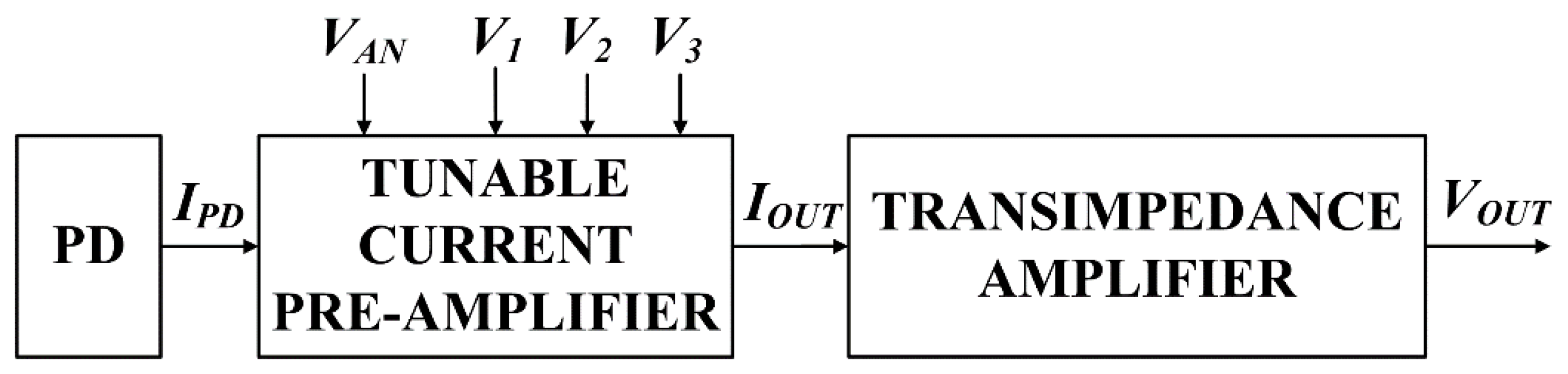
2. Circuit Design and Theory

The overall block scheme illustrating the main stages of the proposed electronic circuit is shown in Figure 1. The photocurrent IPD generated by a PD is the input signal of the TUNABLE CURRENT PRE-AMPLIFIER stage, based on a current mirror architecture, capable to amplify the incoming current signal with a specific gain settable through the external voltages V1, V2 and V3 that are the digital control signals for the electronic circuit coarse gain tuning. An additional external analog control voltage signal VAN is also included to perform fine-tuning of the current gain so providing the amplified output current IOUT. This is the input signal of the subsequent TIA stage and the generated output voltage signal VOUT is obtained by a current-to-voltage amplifier based on a modified Regulated Cascode TIA (RGC-TIA) circuit topology [17,18,19,20,21].
The complete schematic circuit designed at transistor level in TSMC 0.18 µm standard CMOS technology is reported in Figure 2. The circuit has been implemented, simulated, and analyzed in CADENCE Design System environment considering a 1.8 V single supply voltage. More in detail, referring to Figure 2, the first stage of the architecture is the standard electrical model emulating a Si PD that operates in photoconductive regime that is composed by the following elements: an ideal current generator providing the photocurrent IIN proportional to the light power impinging on the PD sensitive area, a junction capacitance CJ, a shunt resistance RSH, and an in-series resistance RS. In addition, the PD cathode terminal represented by the voltage node VBIAS is connected directly to the overall supply voltage VDD = 1.8 V. The PD Anode provides the photocurrent IPD that is the input signal for the subsequent TUNABLE CURRENT PRE-AMPLIFIER block based on a current mirror architecture composed by the transistors M1-M2-M4 and M5 (or M7, or M9) selected by the digital control signal V1 (or V2, or V3, individually activated). These digital control voltages operate on transistors M6, M8, and M10, so allowing to set three different current gains to be selected as a function of the light power illuminating the PD sensitive area. Moreover, the diode-connected transistors M11 and M12 implement the active load of the current mirror architecture. In addition, the analog control signal VAN acts on transistor M3 providing a more accurate and fine-tuning of the overall current gain achieved by this block. The presence of this analog control permits to continuously adjust the effective current gain needed to compensate current offsets and other circuit non-idealities (e.g., current mirror mismatches). Then, the amplified current IOUT flows through the diode-connected transistor M0T of the last stage of the TIA where M2T, having M3T as active load and the source connected to the same TIA input, is properly regulated by a common source voltage amplifier implemented by the M1T and M4T transistors. Finally, the stability of the system is guaranteed by the two capacitances C1 and C2 in feedback connections.
From the complete theoretical analysis, the transimpedance gain of the electronic circuit as function of the frequency is given by the following equation:
Z T O T ( f ) = N g m ( M 3 T )   1 [ 1 + j 2 π f C I N g m ( M 4 T ) g m ( M 2 T ) [ g m ( M 4 T ) + g m ( M 1 T ) ] ] [ 1 + j 2 π f C O U T g m ( M 3 T ) ]
where N is the current gain of the TUNABLE CURRENT PRE-AMPLIFIER block and gm’s are the transconductances of each specified transistor. Moreover, CIN and COUT are the total capacitances at the circuit input and output nodes, respectively. Referring to Figure 2, they are equal to:
{ C I N = C 1 + C 2 [ 1 + g m ( M 1 T ) g m ( M 4 T ) ] + C P A R _ I N C O U T = C L + C P A R _ O U T
where CPAR_IN is the parasitic capacitance at the input of the TIA block and CPAR_OUT the parasitic capacitance at the final output node of the system combined with the load capacitance CL.
The complete layout of the described optoelectronic circuit has been designed in standard TSMC 0.18 μm CMOS technology and is shown in Figure 3a,b, requiring a Si area of 2070 µm2. The overall layout also includes in panel (c) an integrated PD based on a PNP junction with a Si area of 10,000 µm2. The size of the PD sensitive area has been chosen to guarantee a small junction capacitance CJ (8 pF) and standard values of RSH (100 MΩ) and RS (50 Ω) so making this device suitable to detect light pulses in optical biosensing applications. Table 1 reports the sizes of all the employed transistor and the values of the main parameters of the CMOS designed electronic circuit.

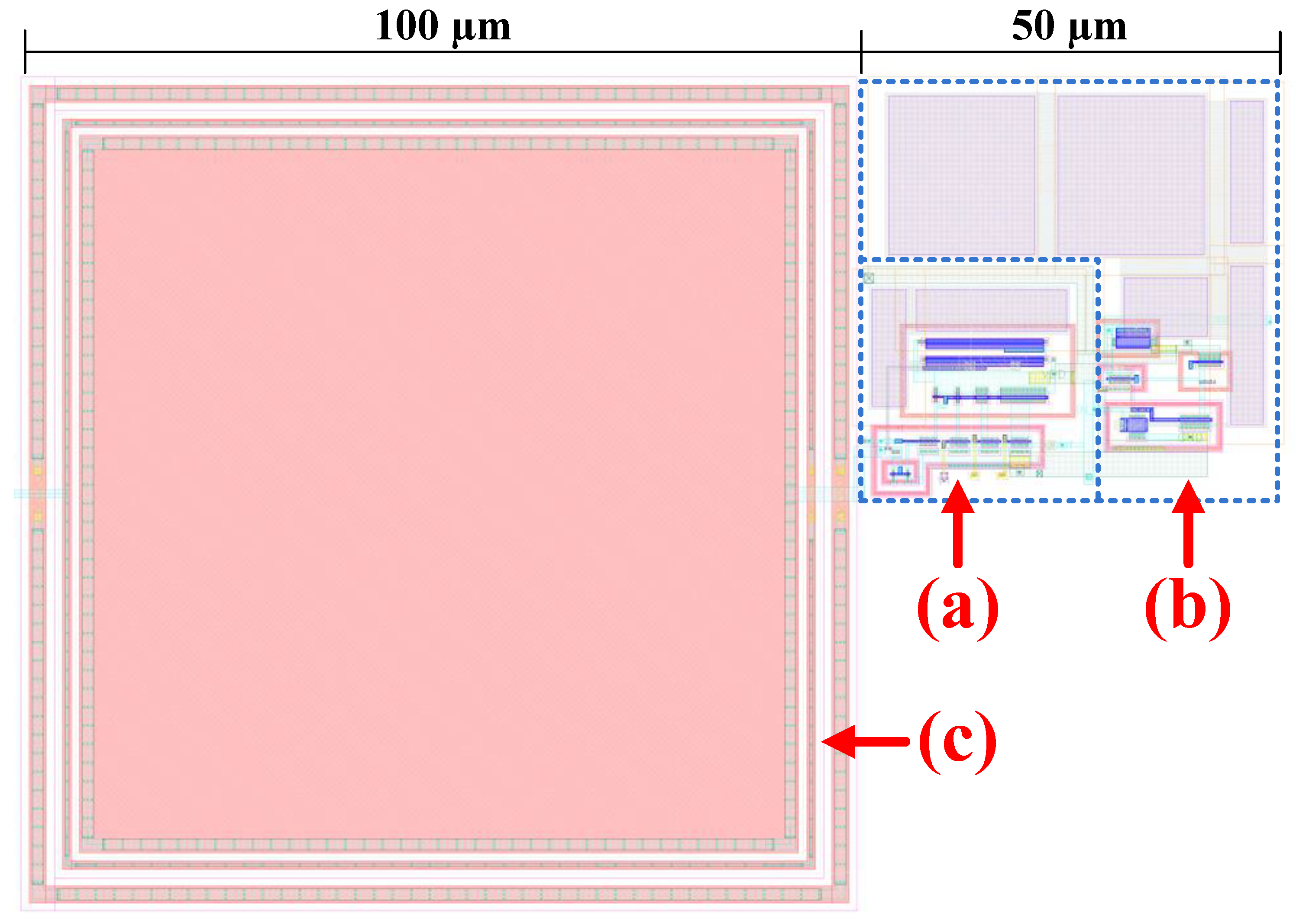
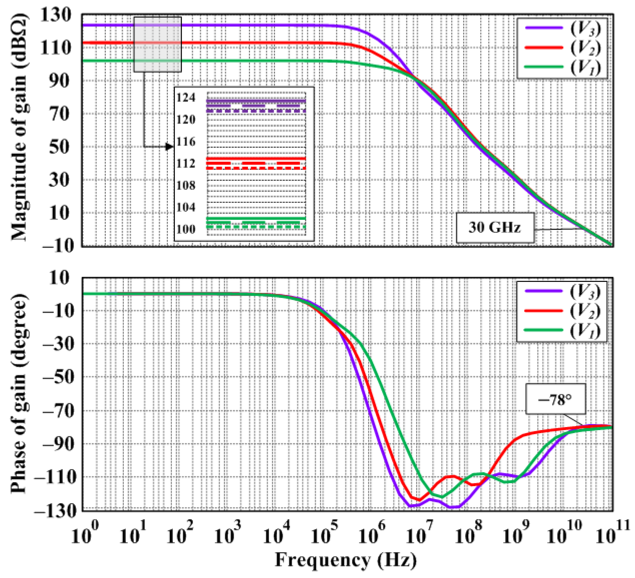
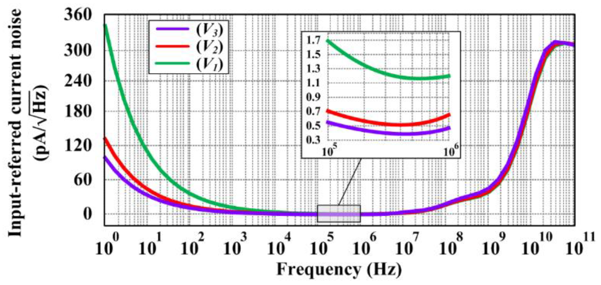
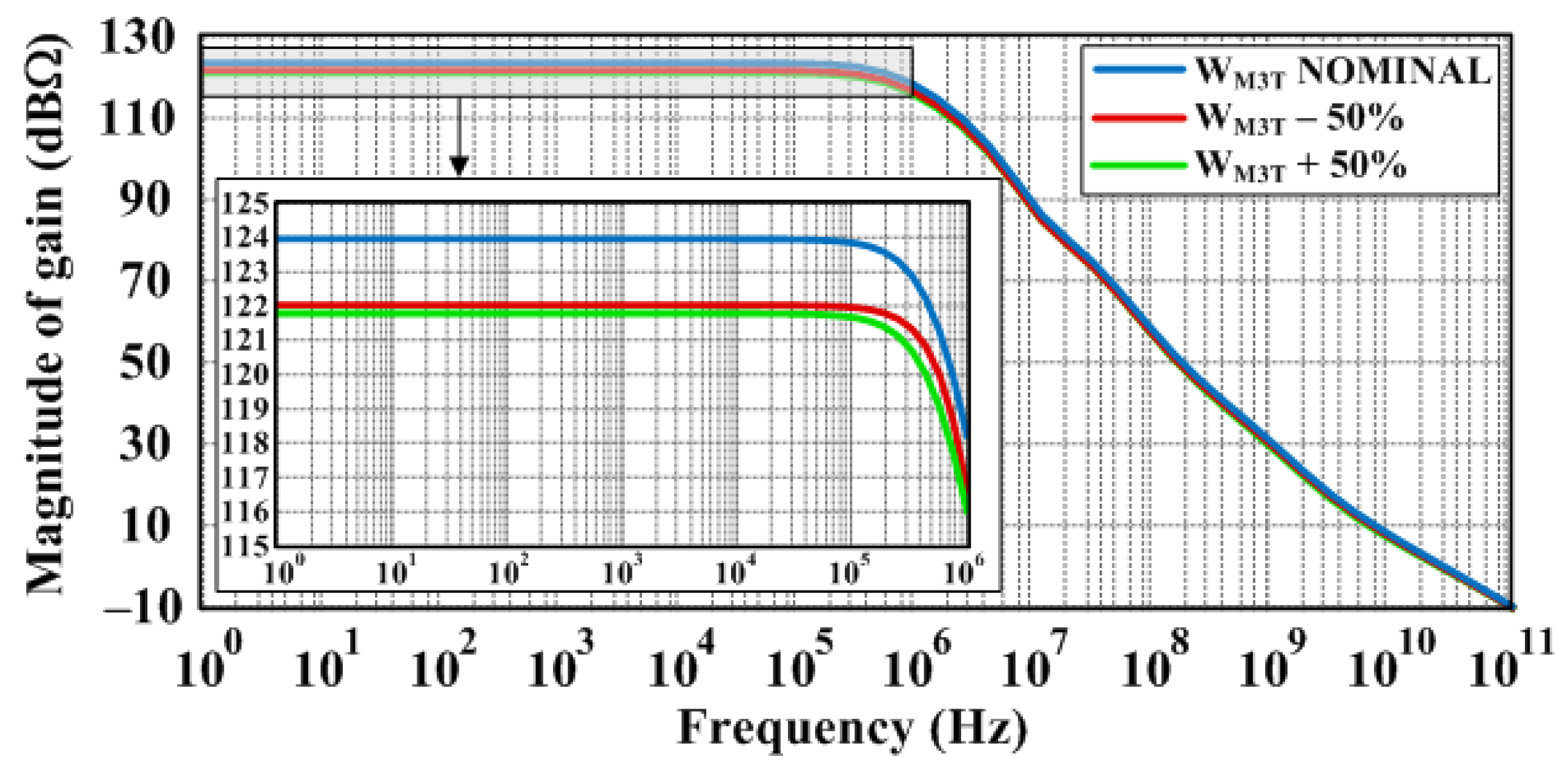
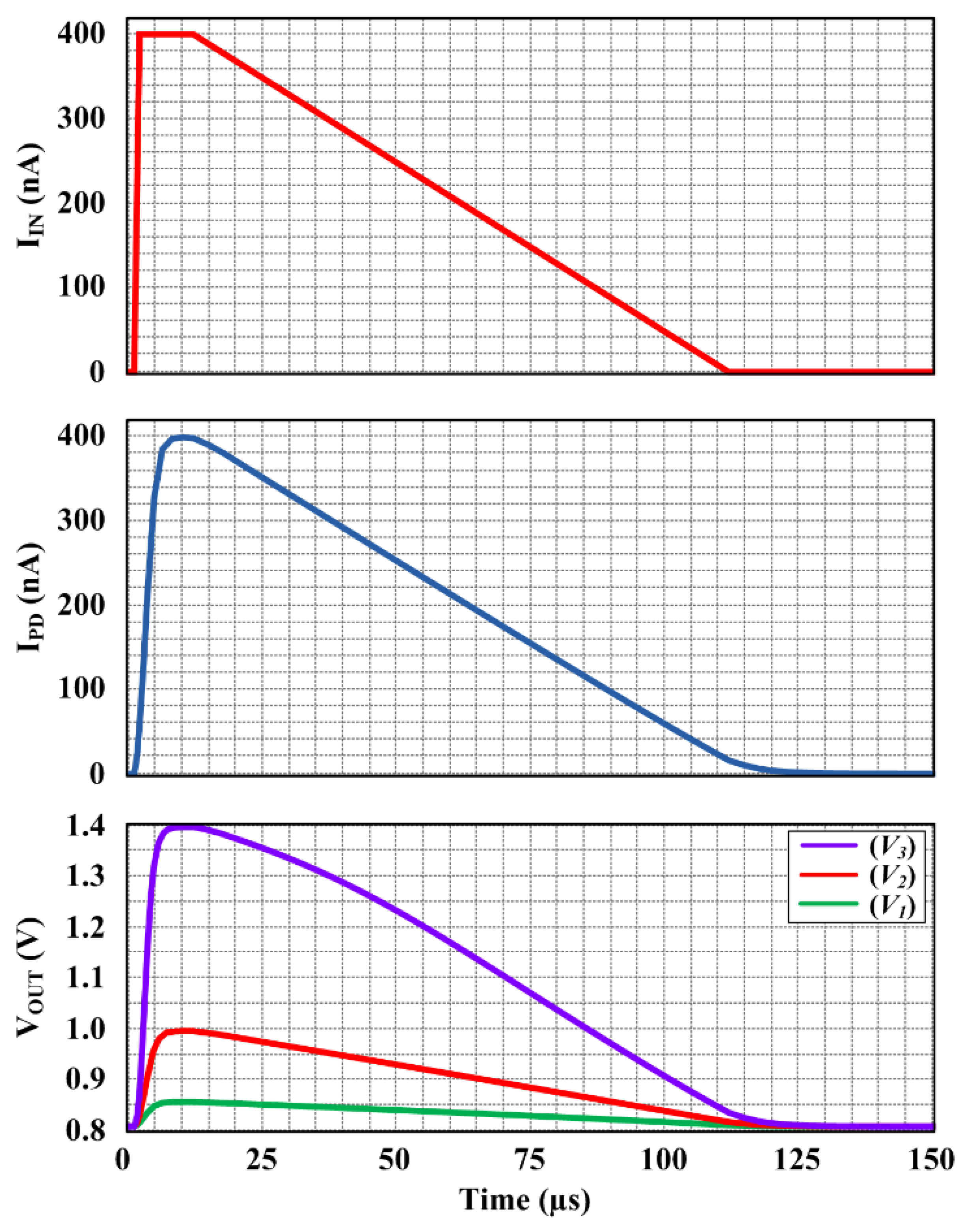
3. Circuit Simulation Results and Discussion

The characteristics and performances of the designed circuit have been evaluated in CADENCE Design Systems environment by performing complete post-layout simulations. More in detail, the transistor sizes and the values of the passive components of the complete circuit reported in Table 1, have been properly chosen and optimized consequentially to the complete theoretical analysis of the circuit and by fully applying standard microelectronic design techniques. In this way, it has been possible to obtain the finest trade-off among all the parameters of the designed circuit with the aim to achieve its best characteristics, especially in terms of: (i) low power consumption; (ii) low noise; (iii) small silicon area; (iv) suitable bandwidth; (v) very high and tunable gain of the circuit powered at 1.8 V single supply voltage; and (vi) capability to operate with nanoampere input current pulses. In addition, the validity and correctness of Equation (1) has been also proven and confirmed through the results achieved by the performed post-layout simulations.
In particular, the small signal frequency analysis of the electronic circuit has been studied and analyzed in the range from 100 Hz to 1011 Hz under three different current gain conditions achieved by varying the external control voltages V1, V2, V3 and VAN of the TUNABLE CURRENT PRE-AMPLIFIER block (see the circuit block scheme of Figure 1 and the schematic of Figure 2). The resulting magnitude and phase values of the transimpedance gain, as a function of the frequency of the input signal, are reported in Figure 4. More in detail, as shown in the upper panel of Figure 4, fixing the value of the analog control voltage VAN = 1.8 V, the resulting circuit bandwidth is about: (i) 555 kHz, corresponding to the maximum transimpedance gain of about 124 dBΩ obtained by setting the control voltages V3 = 1.8 V, V2 = V1 = GND (the purple line); (ii) 650 kHz related to the transimpedance gain of about 113 dBΩ obtained by setting the control voltages V2 = 1.8 V, V3 = V1 = GND (the red line); and (iii) 1.15 MHz associated to the minimum transimpedance gain of about 102 dBΩ obtained by setting the control voltages V1 = 1.8 V, V2 = V3 = GND (the green line). Moreover, for these three values of the transimpedance gain, the inset of the upper panel of Figure 4 also shows the effects of the gain fine-tuning provided by varying the VAN external control voltage. In particular, the continuous lines are the maximum transimpedance gains obtained as previously described, while the dashed and the dotted lines have been obtained by setting VAN = 1.5 V and VAN = 1.2 V, respectively. This fine-tuning capability allows us to control the circuit gain up to about ±2 dBΩ with respect to the maximum/nominal values reported above. Finally, referring to these simulations, the resulting circuit GBW is about 30 GHz with a corresponding phase margin for each gain value of about −78°, as indicated in the low right corner of the lower panel of Figure 4. This result demonstrates that the circuit stability is guaranteed by the presence of the feedback capacitors C1 and C2 that provide a phase response always lower than −130°.
The influence of each circuit parameter on the transimpedance gain has been also investigated and evaluated. Referring to Equation (1), the transimpedance gain mainly depends on the transconductances gm of the transistors composing the circuit and, among them, the most significant one is the transconductance of the transistor M3T (i.e., gm(M3T)). In this regard, specific parametric post-layout simulations have been performed to demonstrate the influence of the variation of the gm(M3T) on the resulting transimpedance gain of the circuit. Therefore, changes of gm(M3T) have been considered by varying of ±50% the transistor width W (i.e., WM3T, from which the gm(M3T) depends on), with respect to its nominal value reported in Table 1. As shown in Figure 5, any variation (positive or negative) of WM3T (and so, of the corresponding gm(M3T)) always provides a significant reduction of the overall transimpedance gain (121.7 dBΩ and 122 dBΩ, for positive and negative variations of WM3T, respectively), with respect to its best value of 124 dBΩ achieved under the chosen operating conditions and circuit device sizes reported in Table 1. In the inset of Figure 5, a magnification of the transimpedance gain, in the reduced range of frequencies from 1 Hz to 1 MHz, has been also reported. Similar analyses have been also performed by changing the transconductance values of the other circuit transistors (i.e., gm(M1T), gm(M2T) and gm(M4T)), always considering variations of ±50% of the transistor widths W, with respect to their nominal values reported in Table 1. In all these last cases, any positive or negative variation of the gm values provides a maximum change of the transimpedance gain lower than ±0.5 dBΩ, with respect to its best value of 124 dBΩ achieved under the chosen operating conditions and device sizes reported in Table 1. Consequently, the dependence of the resulting transimpedance gain from these circuit transistors parameters can be considered negligible. Additionally, these results confirm the best/optimum choice of the complete circuit components and parameters as well as demonstrate the robustness, the stability, and the strong independence of the designed circuit from the technological spread and the process variations [35,36].
In Figure 6, the achieved equivalent input-referred current noise of the circuit is reported. It has been evaluated considering the same frequency range used for the simulations of Figure 4 and Figure 5 and for the three circuit gains controlled by the voltages V1, V2, V3 and fixing VAN = 1.8 V. In the inset of Figure 6 is reported a magnification of the data in a reduced frequency range (i.e., from 100 kHz to 1 MHz) so demonstrating that its minimum value (i.e., the noise floor level), mainly related to the thermal noise contribution, is about: (i) 0.39 pA/ Hz activating the control voltage V3; (ii) 0.53 pA/ Hz activating the control voltage V2; and (iii) 1.2 pA/ Hz activating the control voltage V1. Furthermore, the robustness of the circuit response has been studied by performing Corner Analysis simulations, also including process variations. In this sense, the analysis has been performed by considering temperature variations ranging between −25° to +75 °C and changes of the supply voltage of ±5% with respect to its nominal value (i.e., VDD = 1.8 V). The results of the simulations demonstrate that magnitude and phase of the transimpedance gain, as well as the equivalent input-referred current noise, have a maximum statistical uncertainty of about ±2%.
Additionally, as a case example of the analysis of the electronic circuit response in the time domain, a further series of simulations has also been performed. In particular, a pulsed photocurrent IIN at a repetition rate of 50 Hz has been generated as the ideal current source of the Si PD electrical model shown in Figure 2 [10,37,38,39,40,41]. According to the upper panel of Figure 7, the considered IIN as a function of time has the following main characteristics: rise- and fall-times equal to of 1 μs and 100 μs, respectively; 10 μs pulse-width; 400 nA current peak amplitude; 1 nA minimum current amplitude corresponding to the typical Si PD dark current. These parameters of the photocurrent IIN have been chosen to emulate the behavior of fluorescence or phosphorescence emissions from biomarkers excited by laser pulses used as label-free aptasensors in many applications in biology and medicine for diagnosis and therapeutic control [10,37,38,39,40,41]. Recalling the considered standard values of the PD shunt and series resistances RSH = 100 MΩ and RS = 50 Ω, as well as of the junction capacitance CJ = 8 pF, and taking into account their filtering effect on the pulsed photocurrent IIN, the corresponding effective input current signal IPD of the electronic circuit (see Figure 2) is reported in the middle panel of Figure 7. Moreover, the lower plot of Figure 7 shows the TIA output voltages VOUT as a function of time and for the three different circuit transimpedance gains (as described above), considering the fine-tuning control voltage VAN fixed to 1.8 V. As shown in Figure 7, the circuit output voltage offset is about 810 mV, corresponding to the PD dark photocurrent IIN = 1 nA, while the peak values of the output voltage signals VOUT are about: (i) 860 mV (i.e., 810 mV + 50 mV) by activating the control voltage V1 corresponding to the transimpedance gain of about 126 kΩ (i.e., 102 dB); (ii) 980 mV (i.e., 810 mV + 170 mV) by activating the control voltage V2 corresponding to the transimpedance gain of about 447 kΩ (i.e., 113 dB); and (iii) 1390 mV (i.e., 810 mV + 580 mV) by activating the control voltage V3 corresponding to the transimpedance gain of about 1585 kΩ (i.e., 124 dB). These results are in very good agreement with the transimpedance gain values achieved by performing the frequency domain simulations previously reported in Figure 4. Moreover, referring to the circuit setting with its maximum transimpedance gain of about 124 dB, the achieved equivalent input-referred current noise is about 16.4 pA/√Hz evaluated at the repetition rate equal to 50 Hz of the input pulsed photocurrent IIN.
Besides, from the bias point analysis, the resulting stand-by power consumption of the circuit is about 33 µW with a DC input current IIN = 1 nA (i.e., the PD dark photocurrent). In order to evaluate the circuit power consumption under the AC pulsed regime, the PD pulsed photocurrent IIN previously described has been also considered and under these operating conditions the circuit power consumption varies from 33.1 up to 36.1 µW for the transimpedance gain equal to 102 dB and 124 dBΩ, respectively.
Finally, Table 2 summarize the main characteristics, performances and parameters of the proposed circuit together with those ones of similar solutions reported in the literature. In particular, by comparing the present results with those ones from comparable solutions specifically designed for biomedical applications [24,26], the proposed TIA demonstrates significant improvements especially in terms of the resulting low-power consumption, low input noise, high and tunable transimpedance gain, wide bandwidth, small Si area and Figure of Merit (FOM, as defined in Table 2).

4. Conclusions

The paper reports on the detailed description of a novel architecture of a transimpedance amplifier as an analog front-end circuit operating in low-voltage, low-power regime for wearable, portable and implantable sensor systems capable to operate with nanoampere input current pulses. The circuit has been designed at transistor level in TSMC 0.18 μm standard CMOS technology with a reduced number of components and with an integrated photodiode needed for optoelectronics sensor applications in biomedicine. The complete implemented circuit layout, with a Si area equal to 2070 µm2, is powered at 1.8 V with a maximum power consumption of about 36.1 µW. Moreover, the circuit is capable of providing variable transimpedance gains ranging from 102 to 124 dBΩ, achieved by both coarse- and fine-tuning operations, showing a wide bandwidth up to 1.15 MHz. The main performances of the circuit have been evaluated by performing post-layout simulations in CADENCE Design System employing as input pulsed currents the typical ones generated by a photodiode in optical biosensors optoelectronic sensing systems. Moreover, a complete Corner Analysis including process variations has been performed to validate the robustness of the response of the proposed circuit to variations of the operating temperature from −25° to +75 °C as well as of the power supply voltage of 5% respect to its nominal value. Finally, a summary table is also provided to compare the performances and the characteristics of the proposed circuit with respect to those ones of other similar systems and solutions reported in the literature designed for biomedical applications.

Author Contributions

The authors contributed equally to this work. In particular: G.D.P.S. simulated and implemented the circuit in Cadence, and he contributed to writing and editing the manuscript. A.D.M. developed the new technique/solution and its theory, and he contributed to writing and editing the manuscript and coordinated the manuscript elaboration. G.B. simulated and implemented the circuit in Cadence, and he contributed to writing and editing the manuscript. M.F. analyzed the result data of the system contributing to theoretical discussions, and he contributed to writing and editing the manuscript. E.P. developed the optoelectronic/photonic components for sensing applications and analyzed the result data, and he contributed to writing, editing and supervising the manuscript. U.G. supplied the overall system specifications and constrains and analyzed the result data, and she contributed to writing and editing the manuscript. All authors have read and agreed to the published version of the manuscript.

Funding

This research received no external funding.

Conflicts of Interest

The authors declare no conflict of interest.

References

  1. Iqbal, S.M.A.; Mahgoub, I.; Du, E.; Leavitt, M.A.; Asghar, W. Advances in healthcare wearable devices. NPJ Flex. Electron. 2021, 5, 1–14. [Google Scholar] [CrossRef]
  2. Guk, K.; Han, G.; Lim, J.; Jeong, K.; Kang, T.; Lim, E.-K.; Jung, J. Evolution of Wearable Devices with Real-Time Disease Monitoring for Personalized Healthcare. Nanomaterials 2019, 9, 813. [Google Scholar] [CrossRef] [PubMed] [Green Version]
  3. Cardona, M.; Solanki, V.K.; García Cena, C.E. Internet of Medical Things—Paradigm of Wearable Devices; CRC Press: Boca Raton, FL, USA, 2021; ISBN 9780367272630. [Google Scholar]
  4. Kazanskiy, N.L.; Khonina, S.N.; Butt, M.A.; Ka´zmierczak, A.; Piramidowicz, R. State-of-the-Art Optical Devices for Biomedical Sensing Applications—A Review. Electronics 2021, 10, 973. [Google Scholar] [CrossRef]
  5. Hinrichs, H.; Scholz, M.; Baum, A.K.; Kam, J.W.; Knight, R.T.; Heinze, H.J. Comparison between a wireless dry electrode EEG system with a conventional wired wet electrode EEG system for clinical applications. Sci. Rep. 2020, 10, 1–14. [Google Scholar] [CrossRef]
  6. Dufour, S.; De Koninck, Y. Optrodes for combined optogenetics and electrophysiology in live animal. Neurophotonics 2015, 2, 031205. [Google Scholar] [CrossRef] [Green Version]
  7. Chung, H.U.; Kim, B.H.; Lee, J.Y.; Lee, Y.; Xie, Z.; Ibler, E.M.; Lee, K.; Banks, A.; Jeong, J.Y.; Kim, J.; et al. Binodal, wireless epidermal electronic systems with in-sensor analytics for neonatal intensive care. Science 2019, 363, eaau0780. [Google Scholar] [CrossRef] [Green Version]
  8. Song, S.; Konijnenburg, M.; van Wegberg, R.; Xu, Y.; Ha, H.; Sijbers, W.; Stanzione, S.; Biswas, B.; Breeschoten, A.; Vis, P.; et al. A 769 w battery-powered single-chip soc with ble for multi-modal vital sign monitoring health patches. IEEE Trans. Biomed. Circuits Syst. 2019, 13, 1506–1517. [Google Scholar] [CrossRef]
  9. Kim, H.; Kim, Y.; Mahmood, M.; Kwon, S.; Zavanelli, N.; Kim, H.S.; Rim, Y.S.; Epps, F.; Yeo, W. Fully integrated, stretchable, wireless skin-conformal bioelectronics for continuous stress monitoring in daily life. Adv. Sci. 2020, 7, 2000810. [Google Scholar] [CrossRef]
  10. Costanzo, I.; Sen, D.; Adegite, J.; Rao, P.M.; Guler, U. A Noninvasive Miniaturized Transcutaneous Oxygen Monitor. IEEE Trans. Biomed. Circuits Syst. 2021, 15, 474–485. [Google Scholar] [CrossRef]
  11. Jia, Y.; Guler, U.; Lai, Y.; Gong, Y.; Weber, A.; Li, W.; Ghovanloo, M. A Trimodal Wireless Implantable Neural Interface System-on-Chip. IEEE Trans. Biomed. Circuits Syst. 2020, 14, 1207–1217. [Google Scholar] [CrossRef]
  12. Moreno, J.C.; Bueno, L.; Pons, J.L. Wearable robot technologies. In Wearable Robots: Biomechatronic Exoskeleton; Pons, L.J., Ed.; Wiley: West Sussex, UK, 2008; ISBN 978-0-470-51294-4. [Google Scholar]
  13. Porkodi, S.; Kesavaraja, D. Healthcare Robots Enabled with IoT and Artificial Intelligence for Elderly Patients. In AI and IoT-Based Intelligent Automation in Robotics; Dubey, A.K., Kumar, A., Kumar, S.R., Gayathri, N., Das, P., Eds.; John Wiley & Sons Inc. and Scrivener Publishing LLC: Salem, MA, USA, 2021; pp. 87–108. ISBN 9781119711209. [Google Scholar]
  14. Loeppke, R.R.; Hohn, T.; Baase, C.; Bunn, W.B.; Burton, W.N.; Eisenberg, B.S.; Ennis, T.; Fabius, R.; Hawkins, R.J.; Hudson, T.W.; et al. Integrating health and safety in the workplace: How closely aligning health and safety strategies can yield measurable benefits. J. Occup. Environ. Med. 2015, 57, 585–597. [Google Scholar] [CrossRef] [PubMed] [Green Version]
  15. Sarra, A.; Di Patrizio Stanchieri, G.; De Marcellis, A.; Bordi, F.; Postorino, P.; Palange, E. Laser Transmission Spectroscopy Based on Tunable-Gain Dual-Channel Dual-Phase LIA for Biological Nanoparticles Characterization. IEEE Trans. Biomed. Circuits Syst. 2021, 15, 177–187. [Google Scholar] [CrossRef] [PubMed]
  16. Bag, A.; Lee, N.-E. Recent Advancements in Development of Wearable Gas Sensors. Adv. Mater. Technol. 2021, 6, 2000883. [Google Scholar] [CrossRef]
  17. Kumar, S.; Vanita. A Review of Transimpedance Amplifiers Used in Biomedical Applications. In Proceedings of the IEEE 5th International Conference on Computing Methodologies and Communication (ICCMC), Erode, India, 8–10 April 2021. [Google Scholar]
  18. Atef, A.; Atef, M.; Khaled, E.E.M.; Abbas, M. CMOS Transimpedance Amplifiers for Biomedical Ap-plications: A Comparative Study. IEEE Circuits Syst. Mag. 2020, 20, 12–31. [Google Scholar] [CrossRef]
  19. Lu, Z.; Yeo, K.S.; Lim, W.M.; Do, M.A.; Boon, C.C. Design of a cmos broadband transimpedance amplifier with active feedback. IEEE Trans. Very Large Scale Integr. (VLSI) Syst. 2010, 18, 461–472. [Google Scholar] [CrossRef]
  20. Aflatouni, F.; Hashemi, H. A 1.8 mW Wideband 57 dBΩ Transimpedance Amplifier in 0.13 μm CMOS. In Proceedings of the IEEE Radio Frequency Integrated Circuits Symposium, Boston, MA, USA, 7–9 June 2009. [Google Scholar] [CrossRef]
  21. De Marcellis, A.; Di Patrizio Stanchieri, G.; Palange, E.; Faccio, M.; Constandinou, T.G. An Ultra-Wideband-Inspired System-on-Chip for an Optical Bidirectional Transcutaneous Biotelemetry. In Proceedings of the IEEE Biomedical Circuits and Systems Conference (BioCAS), Cleveland, OH, USA, 17–19 October 2018. [Google Scholar] [CrossRef]
  22. Lin, B.; Atef, M.; Wang, G. 14.85 µW Analog Front-End for Photoplethysmography Acquisition with 142-dBΩ Gain and 64.2-pArms Noise. Sensors 2019, 19, 512. [Google Scholar] [CrossRef] [Green Version]
  23. Atef, M.; Wang, M.; Wang, G. A Fully Integrated High-Sensitivity Wide Dynamic Range PPG Sensor with an Integrated Photodiode and an Automatic Dimming Control LED Driver. IEEE Sens. J. 2018, 18, 652–659. [Google Scholar] [CrossRef]
  24. Konijnenburg, M.; Stanzione, S.; Yan, L.; Jee, D.-W.; Pettine, J.; van Wegberg, R.; Kim, H.; Van Liempd, C.; Fish, R.; Schuessler, J.; et al. A Multi(bio)sensor Acquisition System with Integrated Processor, Power Management, 8 × 8 LED Drivers, and Simultaneously Synchronized ECG, BIO-Z, GSR, and Two PPG Readouts. IEEE J. Solid State Circuits 2016, 51, 2584–2595. [Google Scholar] [CrossRef]
  25. Kang, E.; Tan, M.; An, J.-S.; Chang, Z.-Y.; Vince, P.; Sénégond, N.; Mateo, T.; Meynier, C.; Pertijs, M.A.P. A Variable-Gain Low-Noise Transimpedance Amplifier for Miniature Ultrasound Probes. IEEE J. Solid State Circuits 2020, 55, 3157–3168. [Google Scholar] [CrossRef]
  26. Mathew, M.; Hart, B.L.; Hayatleh, K. Design of a low-current shunt-feedback transimpedance amplifier with inherent loop-stability. Analog. Integr. Circuits Signal Processing 2019, 99, 539–545. [Google Scholar] [CrossRef]
  27. Abu-Taha, J. High Gain, Widebandwidth and Low PowerTransimpedance Amplifier Using DTMOS Transistor. In Proceedings of the IEEE 7th Palestinian International Conference on Electrical and Computer Engineering (PICECE), Gaza, Palestine, 26–27 March 2019. [Google Scholar] [CrossRef]
  28. Lee, S.B.S.; Yeo, K.S. A 4 GHz Single-to-Differential Cross-Coupled Variable-Gain Transimpedance Amplifier for Optical Communication. Electronics 2021, 10, 3042. [Google Scholar] [CrossRef]
  29. Lee, S.B.S.; Liu, H.; Yeo, K.S.; Yu, X.P. Design of differential variable-gain transimpedance amplifier in 0.18-µm SiGe BiCMOS. Electronics 2020, 9, 1058. [Google Scholar] [CrossRef]
  30. Royo, G.; Martinez-Perez, A.D.; Sanchez-Azqueta, C.; Aldea, C.; Celma, S. A Highly Linear Low-Noise Transimpedance Amplifier for Indoor Fiber-Wireless Remote Antenna Units. Electronics 2019, 8, 437. [Google Scholar] [CrossRef] [Green Version]
  31. Van Der Horst, M.J.; Linnenbank, A.C.; Serdijn, W.A.; Long, J.R. Systematic Design of a Transimpedance Amplifier with Specified Electromagnetic Out-of-Band Interference Behavior. IEEE Trans. Circuits Syst. I Regul. Pap. 2010, 57, 530–538. [Google Scholar] [CrossRef]
  32. Valagiannopoulos, C.A.; Tsitsas, N.L. Integral equation analysis of a low-profile receiving planar microstrip antenna with a cloaking superstrate. Radio Sci. 2012, 47, 1–12. [Google Scholar] [CrossRef]
  33. Kassis, M. Moments-Based Techniques for Complex Microelectronic Systems. Ph.D. Thesis, McGill University, Montréal, QC, Canada, 2020. [Google Scholar]
  34. Fikioris, G.; Valagiannopoulos, C.A. Input admittances arising from explicit solutions to integral equations for infinite-length dipole antennas. Prog. Electromagn. Res. 2005, 55, 285–306. [Google Scholar] [CrossRef] [Green Version]
  35. Ziabakhsh, S.; Alavi-Rad, H.; Ahandani, M.A.; Yagoub, M.C.E. Design and optimization of a fully differential CMOS variable-gain lna with differential evolution algorithm for wlan applications. J. Circuits Syst. Comput. 2014, 23, 1450124. [Google Scholar] [CrossRef]
  36. Valencia-Ponce, M.A.; Tlelo-Cuautle, E.; De La Fraga, L.G. On the Sizing of CMOS Operational Amplifiers by Applying Many-Objective Optimization Algorithms. Electronics 2021, 10, 3148. [Google Scholar] [CrossRef]
  37. Berezin, M.Y.; Achilefu, S. Fluorescence Lifetime Measurements and Biological Imaging. Chem Rev. 2010, 110, 2641–2684. [Google Scholar] [CrossRef] [Green Version]
  38. Esipova, T.V.; Karagodov, A.; Miller, J.; Wilson, D.F.; Busch, T.M.; Vinogradov, S.A. Two New “Protected” Oxyphors for Biological Oximetry: Properties and Application in Tumor Imaging. Anal. Chem. 2011, 83, 8756–8765. [Google Scholar] [CrossRef] [Green Version]
  39. Feng, C.; Dai, S.; Wang, L. Optical aptasensors for quantitative detection of small biomolecules: A review. Biosens. Bioelectron. 2014, 59, 64–74. [Google Scholar] [CrossRef] [PubMed]
  40. Cai, T.; Yan, Y.-Z.; Park, Y.; Lee, T.; Peng, D.; Liu, Y.; Ha, C.-S.; Kim, K.C. Phosporescence-Based Flexible and Transparent Optical Temperature-Sensing Skin Capabale of Operating in Extreme Environments. ACS Appl. Polym. Mater. 2021, 3, 2461–2469. [Google Scholar] [CrossRef]
  41. Zhao, E.; Chen, S. Materials with aggregation-induced emission characteristics for applications in diagnosis, therag-nosis, disease mechanism study and personalized medicine. Mater. Chem. Front. 2021, 5, 3322–3343. [Google Scholar] [CrossRef]
Figure 1. Overall block scheme of the proposed electronic circuit.
Electronics 11 01271 g001
Figure 2. Schematic of the proposed electronic circuit designed at transistor level.
Electronics 11 01271 g002
Figure 3. Layout of the CMOS optoelectronic circuit: (a) the TUNABLE CURRENT PRE-AMPLIFIER block; (b) the TIA block; and (c) the integrated PD based on a PNP junction.
Electronics 11 01271 g003
Figure 4. Upper panel: magnitude of the circuit transimpedance gain as function of the frequency for different gain settings by acting on the external control voltages V1, V2, and V3. In the inset, the corresponding fine tuning achieved by varying the control voltage VAN. Lower panel: the corresponding values of the phase of the circuit transimpedance gain.
Electronics 11 01271 g004
Figure 5. Magnitude of the circuit transimpedance gain as function of the frequency and by varying of ±50% the M3T transistor width WM3T (from which the gm(M3T) depends on), with respect to its nominal value reported in Table 1. In the inset, the magnification in the reduced range of frequencies from 1 Hz to 1 MHz.
Electronics 11 01271 g005
Figure 6. Input-referred noise current for the three transimpedance gains activated by the control voltages V1, V2, V3. In the inset, the magnification in the reduce range of frequencies from 100 kHz to 1 MHz.
Electronics 11 01271 g006
Figure 7. Upper panel: pulsed photocurrent IIN generated the PD. Middle panel: input pulsed current signal of the electronic circuit. Lower panel: circuit output voltage for different values of the circuit transimpedance gain.
Electronics 11 01271 g007
Table 1. Transistor sizes and values of the passive components of the electronic circuit.
TransistorSize W/L (µm/µm)
M1, M2, M40.22/0.18
M50.28/0.36
M3, M6, M8, M102.2/0.18
M71.4/0.36
M95.4/0.36
M11, M120.22/14
M0T2/1.6
M1T3.6/0.36
M4T, M2T2.65/0.18
M3T1/4
CL0.7 pF
ComponentValue
C10.3 pF
C21.8 pF
CJ8 pF
RSH100 MΩ
RS50 Ω
Table 2. Main circuit characteristics and its comparison with the state-of-the-art.
[Ref]
Year
[22]
2019
[23]
2018
[24]
2016
[25]
2020
[26]
2019
[This Work]
2021
CMOS Technology (µm)0.350.350.180.180.350.18
Supply Voltage (V)2.0–3.72.7–41.2–1.8±0.9/1.83.31.8
Si Area (mm2)0.641.68 + 0.74 (PD)37.70.12N.A.0.002 + 0.01 (PD)
Achieved ResultsMeasuredMeasuredMeasuredMeasuredSimulatedSimulated
Circuit Operating ModeContinuousPulsedPulsedN.A.SinusoidalPulsed
Transimpedance Gain (dBΩ)135–14214484–127107120102–124
Bandwidth (Hz)1050647 M8.2 M1.15 M (@ 102 dBΩ)
555 k (@ 124 dBΩ)
Power Consumption (µW)153360135520033033.1 (@ 102 dBΩ)
36.1 (@ 124 dBΩ)
Input   Noise   ( pA / Hz )4279271.73.50.39 (@ 124 dBΩ)
1.2 (@ 102 dBΩ)
FOM (Ω × GHz/mW)8.40.241.0630124.8k24.4k (@ 124 dBΩ)
4.4k (@ 102 dBΩ)
Publisher’s Note: MDPI stays neutral with regard to jurisdictional claims in published maps and institutional affiliations.

