Article

Graphene-Based Plasmonic Metamaterial Perfect Absorber for Biosensing Applications

1
Department of Electronic Engineering, Quaid-e-Awam University of Engineering, Science & Technology (QUEST), Nawabshah 67480, Pakistan
2
School of Physics and Electronic Information, Yan’an University, Yan’an 751000, China
3
Department of Electronic Engineering, The Islamia University of Bahawalpur (IUB), Bahawalpur 63100, Pakistan
4
Department of Electronic Engineering, Balochistan University of Information Technology, Engineering and Management Sciences (BUITEMS), Quetta 87300, Pakistan
5
School of Communication and Information Engineering, Xi’an University of Posts & Telecommunications, Xi’an 710121, China
6
School of Electronic Information and Electrical Engineering, Shanghai Jiao Tong University, Shanghai 200240, China
*
Authors to whom correspondence should be addressed.
Electronics 2022, 11(6), 930; https://doi.org/10.3390/electronics11060930
Submission received: 31 January 2022 / Revised: 1 March 2022 / Accepted: 4 March 2022 / Published: 16 March 2022
(This article belongs to the Special Issue Nanosensors: Sensing Principle, System and Application)

Abstract

:
Graphene as a mono-atomic sheet has recently grabbed attention as a material with enormous properties. It has also been examined for enhancing absorbance in the current plasmonic structure. This has led to an increment in the sensitivity of the plasmonic sensors. In this paper, we present theoretical investigation of the novel graphene-based plasmonic metamaterial perfect absorber for biosensing applications. The simulation study performs the analysis of the novel plasmonic metamaterial absorber structure by adding coatings of graphene sheets. Each sheet of graphene enhances absorbance of the structure. In this study, we demonstrate three layers of graphene sheets lead to perfect absorbance (100%) for multiple bands in the visible and near-infrared regions. Furthermore, we also computed the sensitivity of the graphene-based proposed structure by varying the refractive index (RI) of the sensing region from 1.33–1.36 with RI change of 0.01. Proposed fabrication steps for realization of the device are also discussed.

1. Introduction

Biosensors have always contributed significantly in medical diagnostics and environmental monitoring [1,2,3]. The plasmonic-based biosensors have shown excellent performance due to their highly sensitive response with respect to the changes in refractive indices (RIs represented by n) of sensing mediums. The sensing medium refers to the region in the biosensor where bio-receptors (bio-recognition element) are present. When an analyte interacts (couples) with the bio-receptors, the material property (i.e., RI) of the sensing medium is changed. Since each analyte has different characteristics, therefore each analyte would lead to different RI of the sensing medium. The response of plasmonic biosensor depends on the excitation of surface plasmons (SPs) excited by incident light or electrons on the interface between metal and dielectric (for instance sensing medium). SPs are the oscillations/resonances of free electrons in the metal/dielectric interface detected by the dip in the reflected intensity. The induction of dip in the reflectance spectra depends on the properties of the metallic structure and its geometry, and the dielectric analyte characteristics of the sensing medium. If the formers are kept fixed, the later (analyte characteristic) can be analyzed as a function of wavelength or angles of the incident light. As every molecule has different dielectric (material) property (i.e., RI), therefore each molecule can induce reflectance dip at different incident angle or wavelength. Resultantly, the proposed structure can be used as a biosensor by monitoring the variations in the dip of the reflectance spectra. The plasmonic biosensor can be divided into surface plasmon resonance (SPR) biosensor [4,5] and localized surface plasmon resonance (LSPR) biosensors [6,7]. In comparison to the former, the latter has smaller size, is convenient, and shows easy integration with end-to-use equipment and can detect lower concentration of biomolecule [8,9,10,11]. However, to meet the requirements of rapid development of associated disciplines and for early detection of chronic diseases, need of high detection accuracy has increased to a greater extent. Shortcomings with LSPR such as unsatisfactory resonance intensity, smaller peak resonance, wide line-width properties, and many more limit the application of LSPR where high precision is required [12,13]. Therefore, enhancement in the sensitivity of a biosensor is need of the time in order to detect the disease biomarkers early and precisely detect low concentrations of analytes [14]. Therefore, plasmonic structures have been further integrated into metamaterials form due to their strong field localization and enhancement abilities [15]. These are artificial materials with impressive optical characteristics such as negative RI, uncertain dielectric constant, and strong chiral [16,17,18]. Graphene has also been used as an attractive material together with plasmonic sensor [19]. Since every atom in a graphene sheet is a surface atom, therefore molecular interaction and electron transport through graphene can be highly sensitive to adsorbed molecules [20]. Graphene-based optical sensors do not damage living cells as the electrical sensors do [20]. The excellent optical properties of graphene, such as broadband absorbance, saturation absorbance, and fluorescence, gradually attract the attention of scientists [21].
This work focuses on the theoretical analysis of the graphene-based plasmonic metamaterial perfect absorber for biosensing applications in visible and near-infrared region. Section 1 provides the introduction of the plasmonic metamaterial and graphene layers. Section 2 describes the geometry of the proposed structure, simulation setup, and the proposed fabrication steps for the realization of the presented structure. Section 3 discusses outcome analysis of the results of the proposed design and its usage as a biosensor. Section 4 concludes the paper.

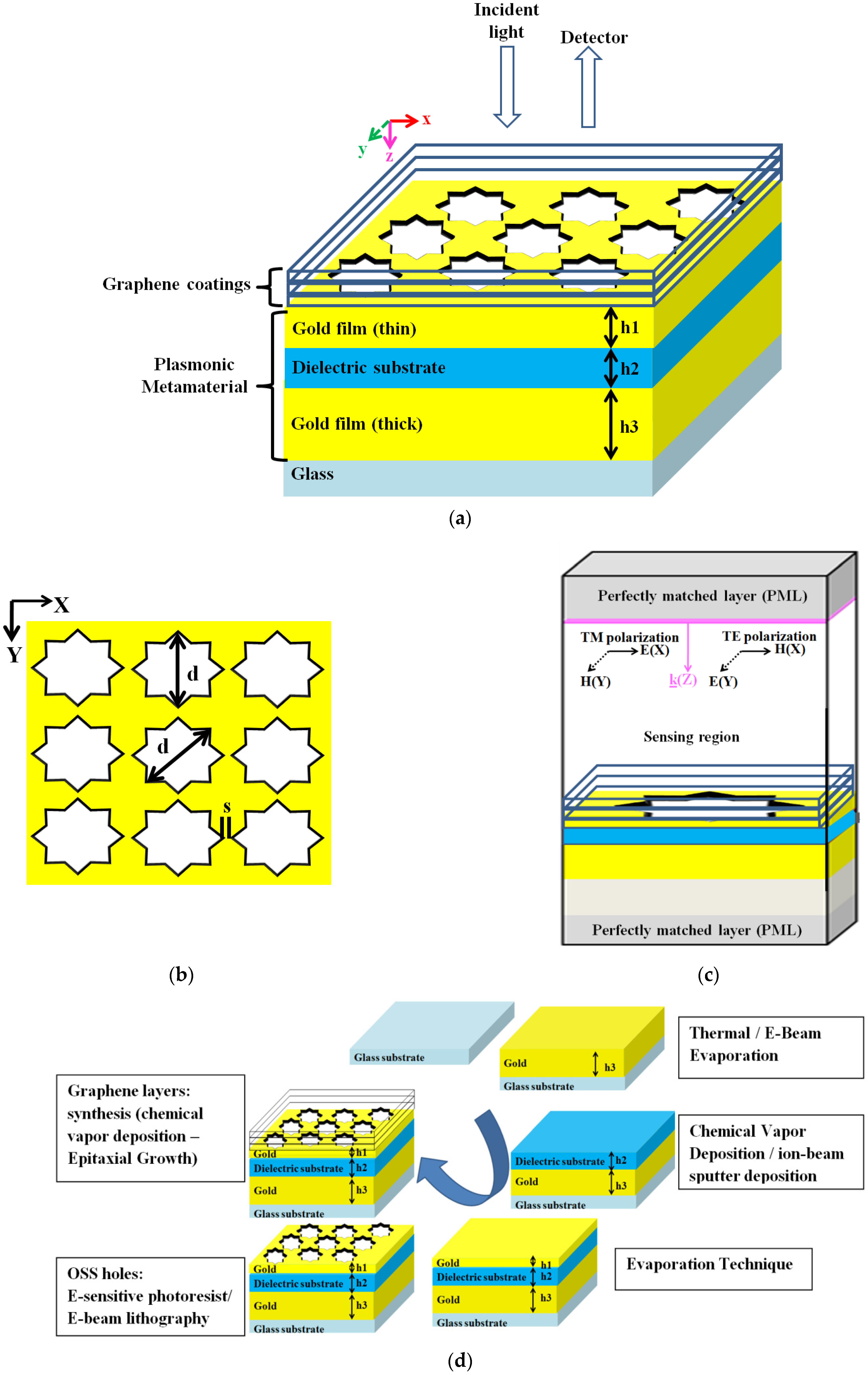
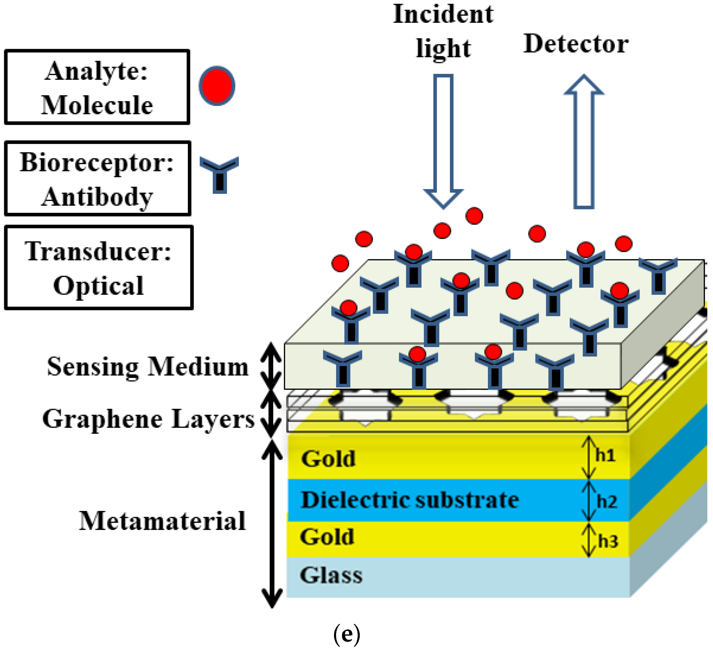
2. Geometry and Method

Graphene-based plasmonic metamaterial perfect absorber (GPMPA) is proposed for the visible and near-infrared region (i.e., 400–1000 nm) placed on a glass substrate as shown in Figure 1. The proposed design is divided into two regions, the first region consists of graphene coatings and the other region consists of a plasmonic metamaterial. Proposed design is analyzed for different numbers of graphene coating layers (N = 1, 2, 3). Each graphene coating has a thickness of 0.34 nm. Graphene layers are used for getting additional absorbance. Plasmonic metamaterial structure comprised of three layers: top, middle, and bottom with thicknesses of h1 (30 nm), h2 (40 nm), and h3 (200 nm), respectively. The top layer consists of a two-dimensional array of octagonal star-shaped (OSS) holes etched into the thin gold film with a separation (s = 13.73 nm), as shown in Figure 1. The OSS is made up of two overlapping square plates with diagonals (d = 226.27 nm). The absorption in the plasmonic structure depends on the excitation/resonance of the electrons in the metals. This leads to the enhancement of the localized electric field surrounding the metal/dielectric interface. If the metallic structure has more corners, then this leads to the excitation of the higher order strong electric dipole resonances (i.e., near fields). As the excitation of the plasmonic modes depends on the geometrical structure, therefore different shapes could lead to different results. Therefore, the OSS holes are used to get the highly localized fields. Middle layer comprises of a thin dielectric substrate used for the confinement of electromagnetic energy. Bottom layer is a thick metallic gold film that eliminates the transmittance of the whole spectrum [22]. The material parameters of the gold and graphene are taken from [22,23], respectively. Whereas the material parameters εr(n) of glass and dielectric substrate are kept as 2.295 (1.515) and 1.9 (1.378).
The simulation setup of the proposed design is illustrated in Figure 1. Finite integration technique (FIT)-based commercially available simulation software (CST Microwave Studio) is used for the electromagnetic analysis. Unit cell of the proposed structure is taken for the simulation to save computational resources. For that purpose, periodic boundary conditions (PBCs) are applied along the X and Y directions of the computational domain with a periodicity (i.e., width of the unit cell/chip) of 240 nm. The PBCs are used to mimic the array of the structure; it helps in reducing the computational requirements of the structure. Absorbing boundary conditions such as perfectly matched layer (PML) is applied along the direction of propagation (i.e., Z-direction). Transverse electric (TE) and transverse magnetic (TM) polarized waves are incident (as excitation) for the spectral calculations between 400 and 1000 nm. Excitation wave is incident with normal incidence (i.e., incident angle = 0°) from the top through a waveguide port, available in CST software. Waveguide port is placed at a distance of λmax (1000 nm) above the proposed structure. In order to analyze the performance behavior of the proposed design, the reflectance (R(λ)), transmittance (T(λ)), and absorbance (A(λ)) spectra are required. This can be achieved by computing reflectance coefficient (S11(λ)) and transmittance coefficient (S21(λ)) through simulation of the whole spectrum. Furthermore, R and T spectra are obtained by (S11)2 and (S21)2, respectively. Whereas A(λ) spectra is obtained by A(λ) = 1 − T(λ) − R(λ).
The fabrication of the proposed biosensor can be carried out using traditional fabrication methods involving thin film deposition and lithography. Graphical representation of fabrication steps can be seen in Figure 1. In sample preparation step, the glass substrate is cleaned and dried to remove any possible contaminations. In the first step, a 200 nm thick gold-film (h3 layer) is deposited on the glass substrate using thermal evaporation or electron beam (E-beam) evaporation technique. In the second step, the 40 nm dielectric layer (h2) can be deposited using chemical vapor deposition or ion-beam sputter deposition technique. In the third step of fabrication, the 30 nm gold-film (h1 layer) is deposited using evaporation technique. Afterwards, the OSS hole can be defined on the gold layer (h1) by applying the E-sensitive photoresist and using E-beam lithography. The solubility of the photoresist is changed when exposed to E-beam which can later be developed to define the patterns. The unwanted portions of the gold-film can be etched by a suitable dry etch technique to etch the desired patterns. Later on, the graphene layers can be grown using bottom-up strategy by synthesis of graphene layer from carbon atoms which can involve various techniques such as chemical vapor deposition and epitaxial growth.
The proposed biosensor with sensing medium, receptor and biomarkers is shown in Figure 1. The optical signal is used as the transduction signal for the detection of biomolecules. The transduction signal is incident with normal incidence (incidence angle = 0°) from the top of the sensing medium. Sensing medium is the region where analytes (biomolecules) are detected. Bio-receptors are the bio-recognition elements that can couple biomolecules. When a biomolecule is coupled with the bio-receptors, the material properties (i.e., RI) of the sensing medium are changed that can be measured with the detector placed at the top of the biosensor.

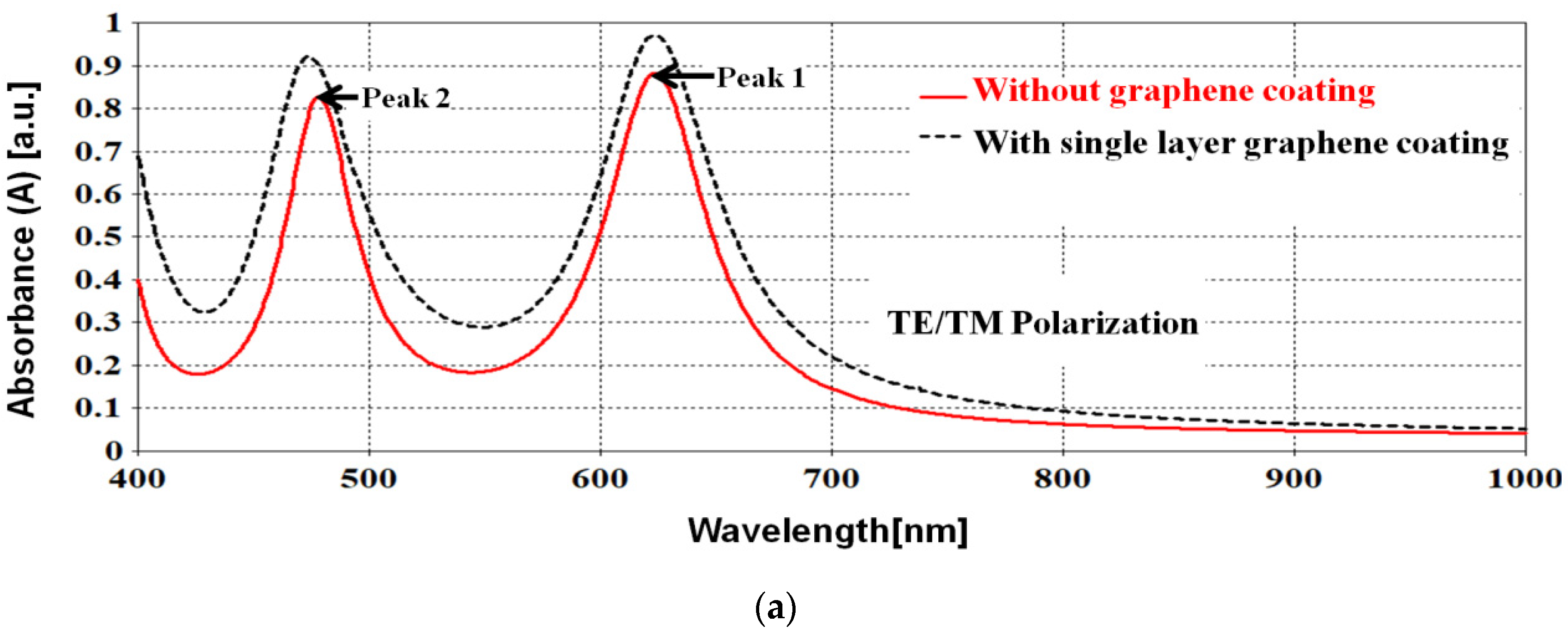
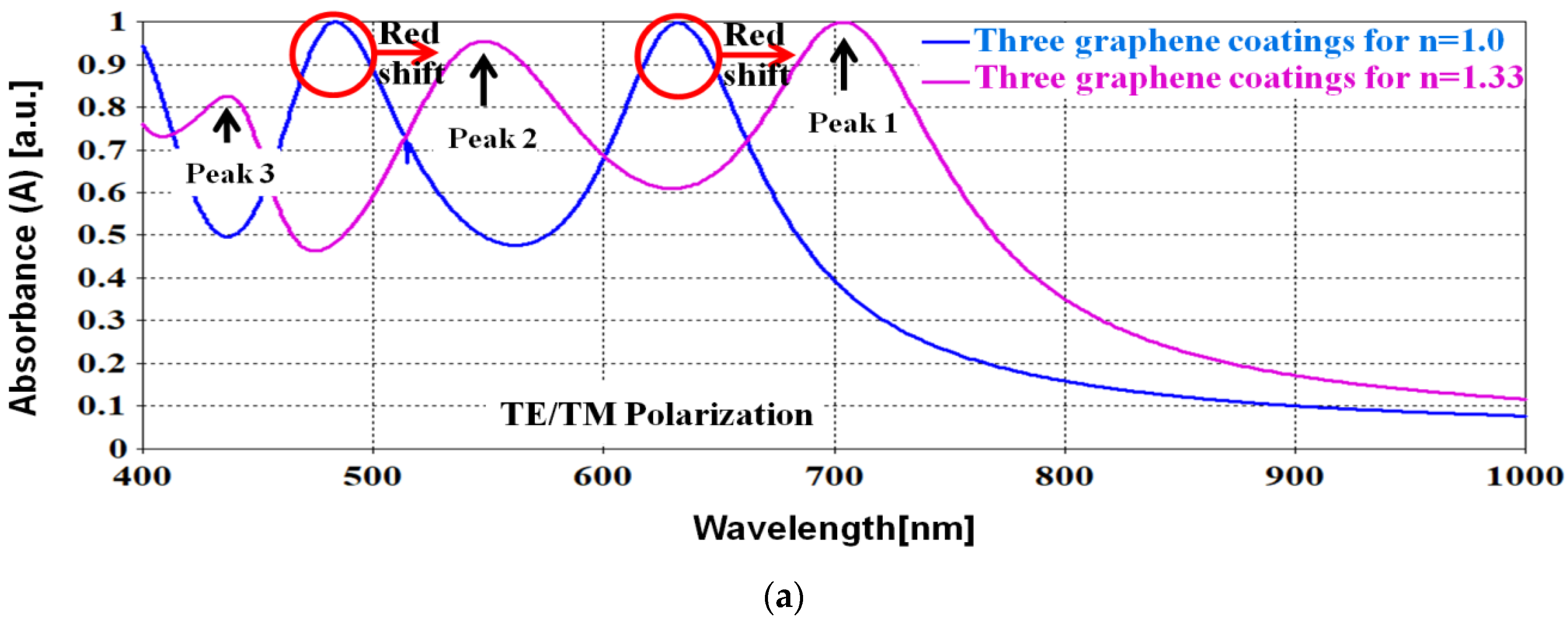
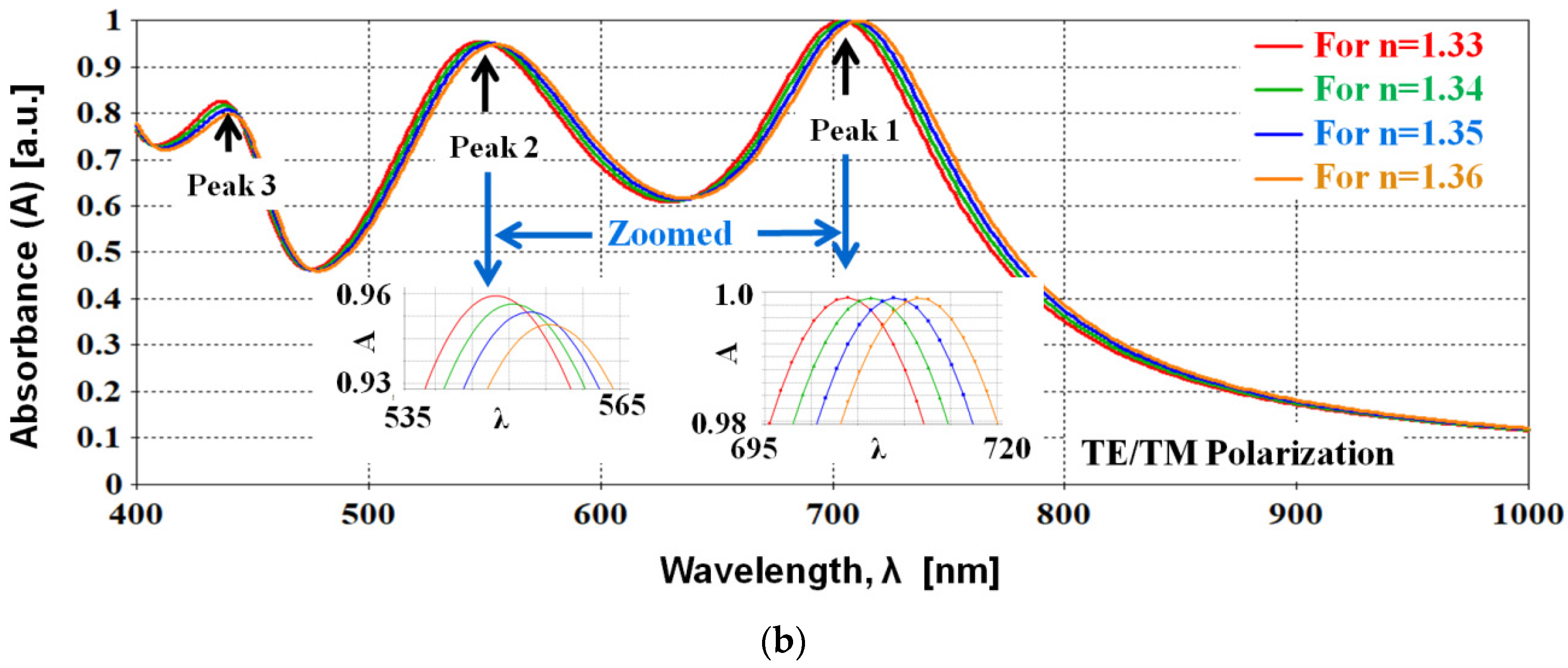
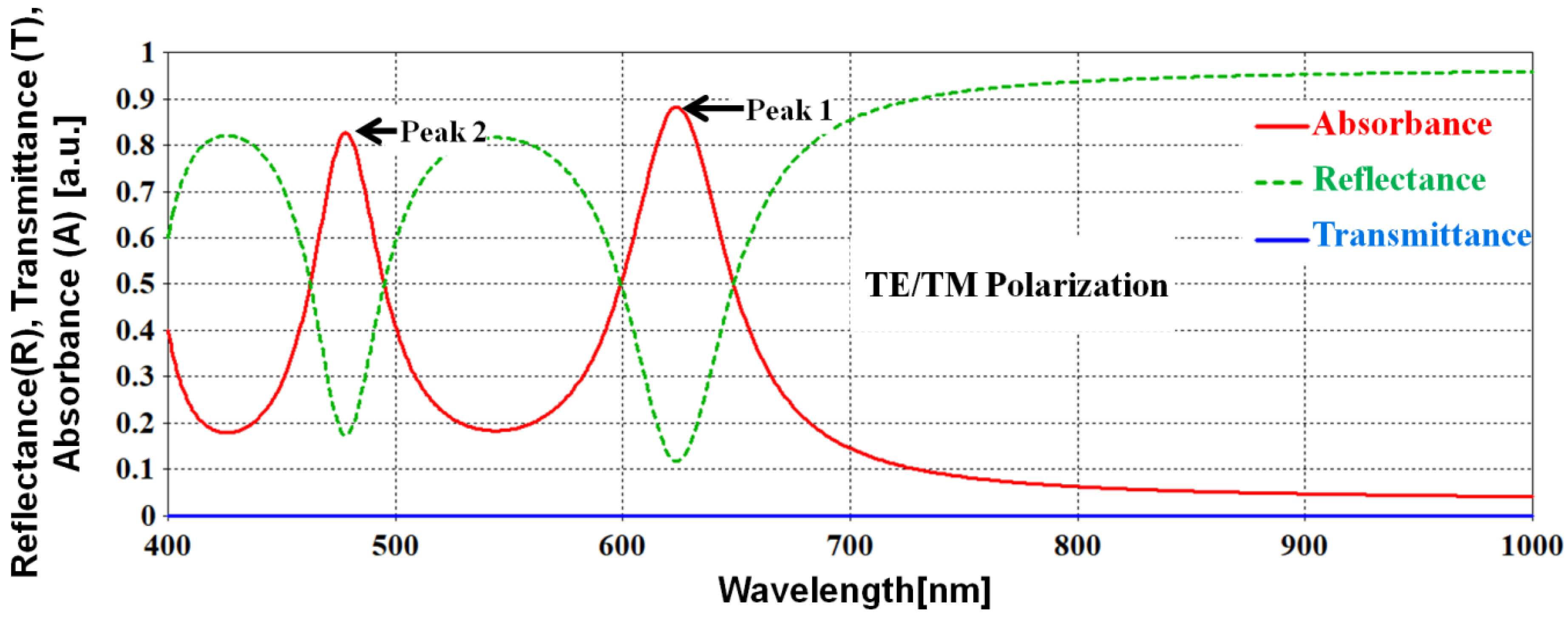
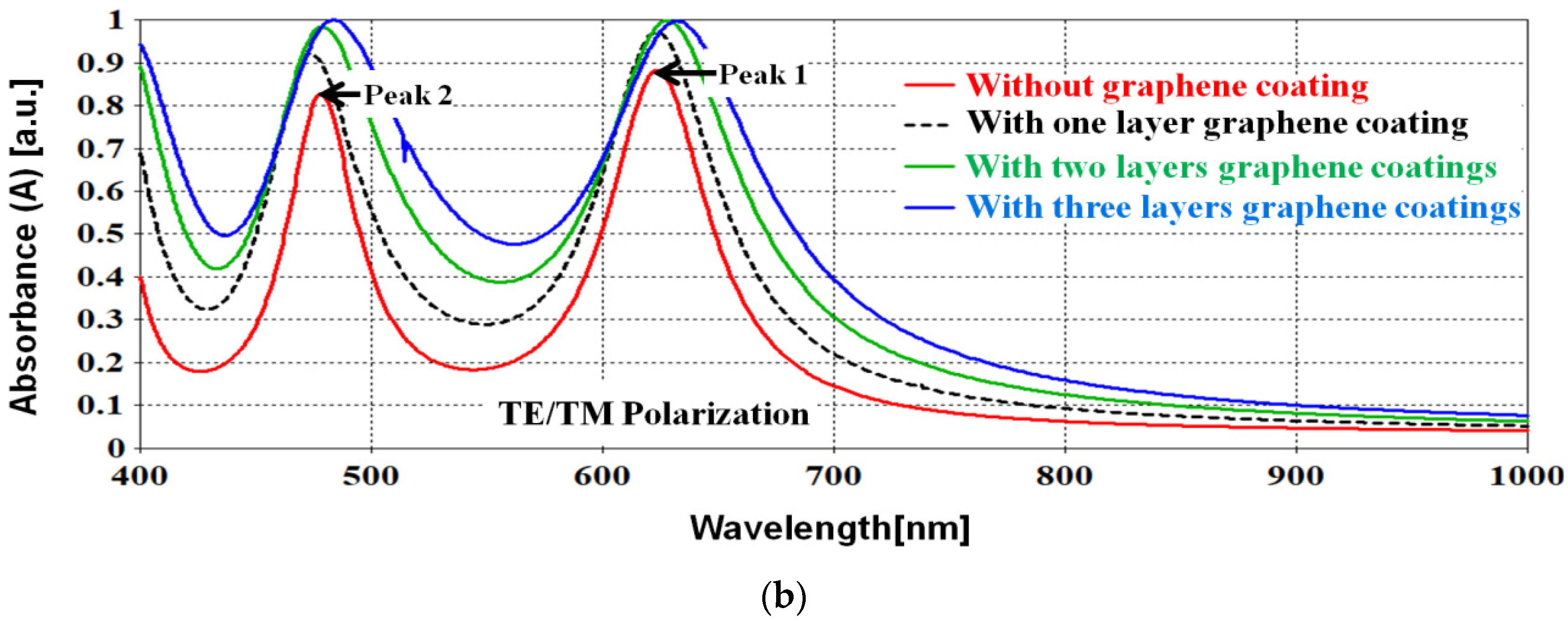
3. Results and Discussion

This work focuses on the numerical analysis of the novel graphene-based plasmonic metamaterial perfect absorber. The simulation results of a unit cell of a proposed device are presented for a wavelength range of 400–1000 nm. The TE and TM wave are excited at normal incidence for a complete spectrum. The R, T, and A spectra are computed for each polarization. The R and T are obtained by squaring separately the S11 and S21, respectively. The A is calculated by using A = 1 − T − R.
Initially the metamaterial perfect absorber is analyzed without graphene layer. The background material (sensing region) between the excitation port and the structure is kept as vacuum (n = 1.0). The R, T, and A spectra for TE and TM polarizations are shown in Figure 2. Both polarizations have similar performance effect, as can be observed in Figure 2 for TE and TM polarizations, respectively. The dashed-green, blue, red curves show R, T, and A spectra, respectively. As can be seen in the blue curve, the transmittance is completely eliminated (i.e., T = 0), which is due to the presence of thick metallic gold layer in the metamaterial absorber. Hence, the A can only be computed from R spectra (A = 1 − R). There are two narrow bands absorbance peaks observed (with more than 80% absorbance). The first peak is found at λ1 = 623.5 nm with 88% absorbance, whereas the second peak is found at λ2 = 478 nm with 83% absorbance.
After analyzing the proposed metamaterial structure, the graphene layer of 0.34 nm is stacked on top of the metallic film having OSS holes. Since, the proposed device is independent of TE and TM polarization, only one polarization is shown in Figure 3. The absorbance spectra of the proposed device with and without single graphene layer are shown in Figure 3. Red curve shows the absorbance spectrum of the device without graphene coating, whereas the dashed-black curve shows the absorbance spectrum of the device with single layer graphene coating. The addition of the single graphene layer has shown 10% increment in the absorbance for both peaks. After that, N number of graphene layers (where N = 0, 1, 2, 3) are stacked on the device. The absorbance spectrum for each layer is also computed, as shown in Figure 3. It is observed that higher absorbance is achieved with increasing number of graphene layers. The first, second, and third graphene sheet enhanced 10%, 6%, 1%, respectively. The perfect absorbance (i.e., 100%) is obtained when three layers of graphene (N = 3) are placed on top of the metallic film having OSS holes, see Figure 3. It is observed that the addition of graphene coating has enhanced the absorbance effect of the device. This in turn improves the adsorption of the biomolecules, leading to an increment in sensitivity of the biosensor, if used in the plasmonic biosensing device, as discussed in [21,22,23]. This is due to the fact that graphene hexagonal cells have stronger and stable π-interaction with carbon-based ring structures [23].
For analyzing the device for biosensing purposes, the RI of the background medium is changed from vacuum (n = 1.0) to water (n = 1.33). Absorbance spectra for n = 1.0 and n = 1.33 are shown in Figure 4. When the RI is changed from 1.0 to 1.33, the absorbance has shown a red-shift (i.e., shifting towards the longer wavelength). First peak (λ1) is red-shifted from 633 nm to 705 nm leading to a shift of 63 nm. Second peak (λ2) is also red-shifted toward the longer wavelength from 484 nm to 546 nm leading to 72 nm shift. Third absorbance peak (λ3) is also observed at 437 nm for n = 1.33 with 82.6% absorbance. This is a red-shifted peak from n = 1.0 which is below 400 nm (visible range). When a light is incident on the plasmonic metamaterial, it causes excitation of SPR depending on the geometrical/material properties of the metamaterial and material properties (RI) of the surrounding environment, i.e., sensing medium. The excitation of SPs is caused when a wave vector of incident light matches with the SPs’ wave vector. Due to this, incident light gets absorbed by the metamaterial structure. As discussed, the excitation of SPs also depends on RI of the surrounding medium. If the RI of the sensing medium changes, excitation of SPs (or absorption) occur at the different wavelengths leading to a shift in the absorption peaks. Figure 4 shows the RI change (Δn) of background material from n = 1.33 to n = 1.36 (Δn = 0.01). Each Δn change of 0.01 red-shifts the absorbance spectra. With this information, the sensitivity (Δλ/Δn) of a device can be computed, which measures the change in output of signal (i.e., absorbance shift) with the change in RI (Δn = 0.01). It is observed that the absorbance spectra for each RI change of 0.01 red-shifts 2.5 nm, this results in the sensitivity of 250 nm/RIU.

4. Conclusions

The absorbance performance of the graphene sheets is analyzed in the novel plasmonic metamaterial structure for the wavelength range of 400–1000 nm (i.e., for visible and near-infrared region). The analysis is performed by using CST Microwave simulation software that utilizes FIT as a numerical technique. First, the absorbance spectra of novel proposed model are studied without graphene sheets. The simulated result shows two absorbance peaks with more than 80% absorbance. The coatings of graphene sheet are added one by one on top of the proposed structure, and the absorbance behavior of peaks is observed. Each sheet of graphene coating added extra absorbance. It is demonstrated that three sheets of graphene coatings lead to perfect absorbance (100%) for both peaks. After getting perfect absorbance, the RI of sensing region is changed from 1.0 to 1.33 to further investigate it as a biosensor. The variation in RI has shown red-shift of the absorbance spectra. The sensitivity (250 nm/RIU) of the proposed device is also computed for biosensing applications. The proposed fabrication steps for the realization of the biosensor structure are also provided. This work has added further knowledge in the plasmonic metamaterial absorber for enhancing absorbance and sensitivity.

Author Contributions

Conceptualization, M.A.K., A.A.J. and Y.K.; methodology, M.A.K., A.A.J. and Y.K.; software, M.A.K., A.A.J. and M.u.R.L.; validation, M.A.K., A.A.J. and M.u.R.L.; formal analysis, M.A.K. and F.Q.; investigation, M.A.K., A.A.J. and M.u.R.L.; resources, X.-C.R., Y.Z. (Yongzhi Zhai) and Y.Z. (Yanmin Zhu); data curation, Y.Z. (Yongzhi Zhai) and Y.Z. (Yanmin Zhu); writing—original draft preparation, M.A.K. and F.Q.; writing—review and editing, M.A.K., F.Q. and M.R.A.; visualization, M.R.A.; supervision, A.A.J. and Y.K.; project administration, A.A.J. and X.-C.R.; funding acquisition, X.-C.R. and M.R.A. All authors have read and agreed to the published version of the manuscript.

Funding

This work is supported in part by the National Nature Science Foundation of China under grant (61861043).

Acknowledgments

The authors acknowledge Quaid-e-Awam University of Engineering, Science and Technology (QUEST), Nawabshah, Pakistan for providing administrative and technical support.

Conflicts of Interest

The authors declare no conflict of interest.

References

  1. Chao, J.; Cao, W.; Su, S.; Weng, L.; Song, S.; Fan, C.; Wang, L. Nanostructure-based surface-enhanced Raman scattering biosensors for nucleic acids and proteins. J. Mater. Chem. 2016, 4, 1757–1769. [Google Scholar] [CrossRef] [PubMed]
  2. Mehrotra, P. Biosensors and their applications—A review. J. Oral Biol. Craniofac. Res. 2016, 6, 153–159. [Google Scholar] [CrossRef] [PubMed] [Green Version]
  3. Rissin, D.M.; Wilson, D.H.; Duffy, D. Chapter 2.13—Measurement of Single Protein Molecules Using Digital ELISA. In The Immunoassay Handbook; Elsevier Science: Amsterdam, The Netherlands, 2013; pp. 223–242. [Google Scholar] [CrossRef]
  4. Lesuffleur, A.; Im, H.; Lindquist, N.C.; Oh, S.-H. Periodic nanohole arrays with shape-enhanced plasmon resonance as real-time biosensors. Appl. Phys. 2007, 90, 243110. [Google Scholar] [CrossRef] [Green Version]
  5. Liu, G.-S.; Xiong, X.; Hu, S.; Shi, W.; Chen, Y.; Zhu, W.; Zheng, H.; Yu, J.; Azeman, N.H.; Luo, Y.; et al. Photonic cavity enhanced high-performance surface plasmon resonance biosensor. Photonics Res. 2020, 8, 448–456. [Google Scholar] [CrossRef]
  6. Chuang, P.-C.; Liao, P.-C.; Chen, Y.-F. Enhancing the sensitivity of localized surface plasmon resonance (LSPR) biosensors using nanorods and DNA aptamers. In Proceedings of the SPIE BiOS, San Francisco, CA, USA, 7–12 February 2015; p. 93400T. [Google Scholar] [CrossRef]
  7. Takei, H.; Bessho, N.; Ishii, A.; Okamoto, T.; Beyer, A.; Vieker, H.; Gölzhäuser, A. Enhanced Infrared LSPR Sensitivity of Cap-Shaped Gold Nanoparticles Coupled to a Metallic Film. Langmuir 2014, 30, 2297–2305. [Google Scholar] [CrossRef]
  8. Chien, M.-H.; Brameshuber, M.; Rossboth, B.K.; Schütz, G.J.; Schmid, S. Single-molecule optical absorption imaging by nanomechanical photothermal sensing. Proc. Natl. Acad. Sci. USA 2018, 115, 11150–11155. [Google Scholar] [CrossRef] [Green Version]
  9. Nunna, B.B. Detection of cancer antigens (CA-125) using gold nano particles on interdigitated electrode-based microfluidic biosensor. Nano Converg. 2019, 6, 3. [Google Scholar] [CrossRef]
  10. Sagle, L.B.; Ruvuna, L.K.; Ruemmele, J.A.; Van Duyne, R.P. Advances in localized surface plasmon resonance spectroscopy biosensing. Nanomedicine 2011, 6, 1447–1462. [Google Scholar] [CrossRef] [Green Version]
  11. Willets, K.A.; Van Duyne, R.P. Localized Surface Plasmon Resonance Spectroscopy and Sensing. Annu. Rev. Phys. Chem. 2007, 58, 267–297. [Google Scholar] [CrossRef] [Green Version]
  12. Chen, S.; Svedendahl, M.; Van Duyne, R.P.; Käll, M. Plasmon-Enhanced Colorimetric ELISA with Single Molecule Sensitivity. Nano Lett. 2011, 11, 1826–1830. [Google Scholar] [CrossRef]
  13. Liang, Y.; Zhang, H.; Zhu, W.; Agrawal, A.; Lezec, H.; Li, L.; Peng, W.; Zou, Y.; Lu, Y.; Xu, T. Subradiant Dipolar Interactions in Plasmonic Nanoring Resonator Array for Integrated Label-Free Biosensing. ACS Sens. 2017, 2, 1796–1804. [Google Scholar] [CrossRef] [PubMed]
  14. Xu, T.; Geng, Z. Strategies to improve performances of LSPR biosensing: Structure, materials, and interface modification. Biosens. Bioelectron. 2021, 174, 112850. [Google Scholar] [CrossRef] [PubMed]
  15. Chen, T.; Li, S.; Sun, H. Metamaterials Application in Sensing. Sensors 2012, 12, 2742–2765. [Google Scholar] [CrossRef] [PubMed]
  16. Dolling, G. Simultaneous Negative Phase and Group Velocity of Light in a Metamaterial. Science 2006, 312, 892–894. [Google Scholar] [CrossRef] [Green Version]
  17. Hoffman, A.J.; Alekseyev, L.; Howard, S.S.; Franz, K.J.; Wasserman, D.; Podolskiy, V.A.; Narimanov, E.E.; Sivco, D.L.; Gmachl, C. Negative refraction in semiconductor metamaterials. Nat. Mater. 2007, 6, 946–950. [Google Scholar] [CrossRef]
  18. Smith, D.R. Metamaterials and Negative Refractive Index. Science 2004, 305, 788–792. [Google Scholar] [CrossRef] [Green Version]
  19. Yi, Z.; Chen, J.; Cen, C.; Chen, X.; Zhou, Z.; Tang, Y.; Ye, X.; Xiao, S.; Luo, W.; Wu, P. Tunable Graphene-based Plasmonic Perfect Metamaterial Absorber in the THz Region. Micromachines 2019, 10, 194. [Google Scholar] [CrossRef] [Green Version]
  20. Yi, Z.; Liang, C.; Chen, X.; Zhou, Z.; Tang, Y.; Ye, X.; Xiao, S.; Yi, Y.; Wang, J.; Wu, P. Dual-Band Plasmonic Perfect Absorber Based on Graphene Metamaterials for refractive Index Sensing Application. Micromachines 2019, 10, 443. [Google Scholar] [CrossRef] [Green Version]
  21. Li, Z.; Zhang, W.; Xing, F. Graphene Optical Biosensors. Int. J. Mol. Sci. 2019, 20, 2461. [Google Scholar] [CrossRef] [Green Version]
  22. Jamali, A.A.; Witzigmann, B. Plasmonic Perfect Absorbers for Biosensing Applications. Plasmonics 2014, 9, 1265–1270. [Google Scholar] [CrossRef]
  23. Wu, L.; Chu, H.S.; Koh, W.S.; Li, E.P. Highly Sensitive Graphene Biosensors Based on Surface Plasmon Resonance. Opt. Express 2010, 18, 14395–14400. [Google Scholar] [CrossRef] [PubMed]
Figure 1. Geometry and method of the proposed graphene-based plasmonic metamaterial perfect absorber; (a) perspective view; (b) top view of the 2-dimensional OSS holes embedded in a gold film; (c) simulation setup of a unit cell; (d) proposed fabrication steps for the realization; (e) proposed biosensor showing sensing surface, receptors, and biomarkers.
Electronics 11 00930 g001aElectronics 11 00930 g001b
Figure 2. Reflectance (dashed-green), transmittance (blue), and absorbance (red) spectra with TE/TM polarizations for the proposed structure.
Electronics 11 00930 g002
Figure 3. Comparison of absorbance spectra of the proposed model without and with graphene coatings; (a) proposed model without graphene layer coating (red curve) and with single layer graphene coating (black dashed curve); (b) for N = 0, 1, 2, and 3 layers (where N is the number of graphene layers).
Electronics 11 00930 g003aElectronics 11 00930 g003b
Figure 4. Absorbance spectra for different RI (n): (a) 1.0 and 1.33; (b) 1.33 to 1.36 (insets show the zoomed pictures of both peaks, left (peak 2), right (peak 1)).
Electronics 11 00930 g004aElectronics 11 00930 g004b
Publisher’s Note: MDPI stays neutral with regard to jurisdictional claims in published maps and institutional affiliations.

