Abstract
The radio frequency (RF) laboratory hosted in the Corpuscular Physics Institute (IFIC) of the University of Valencia is designed to house a high-power and high-repetition-rate facility to test normal conduction RF accelerator cavities in the S-Band (2.9985 GHz) in order to perform R&D activities related to particle accelerator cavities. The system, which manages the entire process of RF signal generation, data acquisition and closed-loop control of the laboratory, is currently based on a modular and compact PXI platform system. This contribution details the development of a platform with similar features, but which is based on open architecture standards at both the hardware and software level. For this purpose, a complete system based on the μTCA platform has been developed. This new system must be able to work with accelerator cavities at other operating frequencies, such as 750 MHz, as well as to explore different options at firmware and software levels based on open-source codes.
1. Introduction
The IFIC [1] high-gradient radio frequency (RF) laboratory is designed to house high-power infrastructure with which to test S-Band normal conduction RF accelerator cavities. The main objective of the facility is to develop S-Band high-gradient accelerator structures and contribute to the study of very high field non-linear electromagnetic phenomena, also known as breakdowns.
The type of structures that can be studied in the laboratory are copper-made traveling wave accelerating cavities for linear accelerators with a central operating frequency of 2.9985 GHz. These cavities work in pulsed mode at a repetition frequency of up to 400 Hz and with a duty cycle of two parts per thousand. This means that during a period of 2.5 ms, the cavities are fed with the RF signal only for a time of up to about 5 μs, i.e., the duration of the RF pulse which accelerates the beam of particles through the cavity. The interest is in this type of accelerator structure because linear accelerators, unlike ring accelerators, are of special importance for medical applications as they can provide a high degree of flexibility for treatments [2]. For example, linear accelerators for protons or carbon ions that operate at a 100–400 Hz repetition rate can vary the energy (and intensity) of the beam during the 2.5–10 ms time gap which separates two consecutive pulses. This allows complex and more precise treatments that are not possible otherwise.
The design of the laboratory has been carried out through a collaboration between IFIC and CERN’s CLIC-RF group [3]. A high-power RF system and its corresponding control and acquisition systems have been built. This allows research activities to be carried out, as well as the testing of different cavity geometries and configurations.
The RF and control electronics system described in this publication, the so-called low-level RF (LLRF) system, is similar to many current installations in particle accelerators, in both test and real operations. The role of the LLRF system is to carry out a precise control of amplitude and phase of the EM field inside the cavity, which is of primary importance to ensure field stability throughout the acceleration process. Several external factors can disturb the field during operation, and these sources of non-ideality must be tackled by the LLRF system, which implements a closed-loop control in order to stabilize the field parameters in the cavity. Therefore, this system requires the simultaneous data acquisition of multiple ADC channels and real-time signal processing between pulses, together with highly demanding requirements in terms of reliability, availability and reconfigurability. Initially, many of these were based on custom hardware developments using architectures such as VME, as well as in other modular platforms with limited reconfigurability, such as nuclear instrumentation modules (NIM), similar to the designs used at the LHC [4]. Next, other platforms, such as CompactPCI (cPCI) [5] and VXI [6], were also used in the field of particle accelerators and are still in operation, while others that have been built to have low cost and long lifecycles, such as PXI, have not been able to establish themselves as a reference architecture. However, the new generation of modular systems capable of higher performance in terms of timing accuracy, transfer speeds, frequency range, processing capability and programmability, based on the μTCA open standard [7], has been emerging as the platform of choice for LLRF systems in the particle accelerator world over the last few years.
μTCA is a descendant of ATCA. It is built for more compact and less expensive systems, without affecting reliability or data throughput, and has been promoted and supported by DESY through its MicroTCA Technology Lab. The standard was first ratified in 2006 and, subsequently, several extensions have been added to it, of which the so-called μTCA.4 is of particular interest and is being widely used for particle accelerators and other large scientific facilities. The advantages it offers, and for which it stands out, are [8]: it combines high-precision measurement with low-latency processing; it is designed for the parallel processing of a large number of RF signals; the standard is very compact; it offers high reliability and availability thanks to its redundancy; it allows for remote software upgrades and maintenance; modularity and scalability permit easy hardware system upgrades; it offers a computer architecture consistent with the modular open systems approach (MOSA) for reduced lifecycle costs; there is an increasing number of suppliers offering new modules with new capabilities for a broad range of industrial and scientific applications in and with the latest FPGA devices.
In the specific case of this project, the reason for exploring the use of a μTCA system is motivated by certain limitations found in the current PXI system related to: the obligation to program the entire system using labVIEW, with the advantages and disadvantages that this entails; the limited ability to control what and how algorithms are implemented in FPGAs; it is a closed standard and, in this case, there is an exclusive dependence on a hardware vendor; and finally the cost, which, in the case of the system described in this contribution, is above EUR 100 k.
However, systems based on μTCA.4 are becoming more widely used in the particle accelerator community mainly thanks to their high performance and their high integration in a compact format [7]. It is certainly also considered to be an expensive and difficult standard to develop on, but one which offers reasonable flexibility, and it is possible to find an incipient number of providers and modules based on the FMC standard (FPGA mezzanine carrier) on the market, which allow the diversification of the functionality of the system. In addition, the cost of a system with functionality comparable to that of the PXI system described in this contribution costs around half.
The new acquisition system described in this publication, which is based on the μTCA platform, is intended to be used for different operating conditions and for different operating frequencies. In particular, the compact RFQ (radio frequency quadrupole) cavities that operate at 750 MHz and which are used as the first acceleration stage in linear accelerators [9] are of special interest.
First, the laboratory high-power RF system will be introduced. The following two sections are dedicated to describing the LLRF and the details of its current implementation based on the PXI platform. Subsequently, a new LLRF proposal based on the μTCA platform and the details of the implementation will be presented. After that, the real-time control algorithms running in the embedded system will be described. Finally, the possibilities to develop the firmware and software of the new system based on open standards will be discussed.
2. Materials and Methods
2.1. High Power RF System
The design of the RF laboratory is inspired by the set-up of the Xbox-3 test facility [10] at CERN, and it has been adapted to the S-Band frequency. The design and all the components are shown in Figure 1. Two pulsed S-Band klystron-type amplifiers fed by two solid-state modulators are used. In a first stage, the RF inputs to the klystron come from a 400 W solid-state preamp with ~56 dB gain. The input to these amplifiers is a pulsed RF signal (2.9985 GHz) of 5 μs in length generated by the LLRF system. The klystrons can provide a maximum RF power of 7.5 MW with a pulse length of up to 5 μs and a repetition frequency of up to 400 Hz. The power output of both klystrons is combined in a hybrid of 3 dB to achieve a power of up to 15 MW alternately, depending on the relative phase between the two incoming RF waves, at the cost of reducing the repetition rate by half, that is, 200 Hz. The RF power is then led through WR-284 waveguides to the structure under test (DUT) installed inside the bunker, which is equipped with the experimental setup required for breakdown studies.
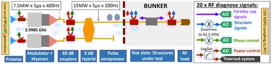
Figure 1.
High-power RF system setup.
The RF power amplitude of each klystron can be controlled pulse by pulse, providing the flexibility to test different prototype designs or structures exhibiting different conditioning states. Directional couplers are used to diagnose direct and reflected RF signals in the waveguide system and the structure under test.
Figure 1 outlines the LLRF subsystem, which will be described in the next section, although it is briefly introduced here to clarify what the interrelation between it and the high-power subsystem consists of. As indicated in the figure, the LLRF system is in charge of generating the RF signal that will reach the DUT and, therefore, defines the RF power that will drive it. The figure also indicates, by using arrows of different colors, all the signals which are read by the acquisition system and that are used for the control or monitoring purposes of the system. These signals are extracted through directional couplers in different stages of the system, after which down-mixing is carried out and, subsequently, they are sampled to extract their amplitude and phase in order to be used for controlling the system. These RF signals will also be able to generate, through the use of logarithmic RF amplifiers, fast interlock signals that will make it possible for the LLRF to disable the RF injection or even completely stop system operations. Finally, and although it is not shown in the figures, due to the amplifiers’ pulsed mode operation, the LLRF must send the trigger signals with the appropriate delays and durations to enable the equipment only during the necessary time window, and so the system works synchronously as a whole.
2.2. LLRF Subsystem
The LLRF subsystem is the “brain” of the entire system and, therefore, is the most critical element from an operational point of view. It comprises RF generation, the entire DAQ chain, and some additional components, such as down-mixers and logarithmic power detectors. The generation of the RF signals is based on a commercial programmable vector and arbitrary signal generators at a sampling rate of 250 MSPS (megasamples per second) with a range of operating frequencies from 750 MHz to 3 GHz, and with a bandwidth of about ~200 MHz, which is considered to be sufficient to generate pulsed amplitude and phase modulated signals, with a duration that ranges from tens of nanoseconds to milliseconds. Data acquisition is based on ADCs with acquisition rates which range from 100 MSPS to 500 MSPS. The choice of the ADC features is mainly based on system requirements and market availability. In addition to the RF generator and the ADCs, two further elements are required: a module based on programmable digital logic to generate the synchronization and trigger signals that are normally needed by other components of the experimental system due to pulsed mode operations, and a CPU unit to read, process and manage all the data in real time for system control.
Currently, the LLRF subsystem is built using a compact, high-bandwidth, modular PXI platform. This modular system is highly configurable and flexible, allowing real-time processing thanks to its architecture based on FPGA (field programmable gate array). As indicated in Figure 1, the RF generators provide the RF pulse at the cavity resonance frequency, in this case 2.9985 GHz, which feeds the 200 W preamps, and then continues to the klystrons. These generators define the repetition rate, maximum power, pulse length, pulse shape and the phase required by the pulse compressor and the 3 dB hybrid. Direct and reflected RF signals are read from the 60 dB directional couplers and mixed at an intermediate frequency (IF) so that ideally 4 samples per RF period can be acquired by fast ADCs. The IF signals are sent either to the fast acquisition channels for further monitoring and analysis, or they are sent (only the reflected signals) to the interlock system.
In the high-rate acquisition modules, which contain an FPGA, real-time pre-processing is performed to achieve a data reduction of the front-end signals of the read channels. This pre-processing consists of digital low-pass filtering, digital I-Q demodulation and breakdown detection. The acquisition speed is given by the need for a high temporal resolution when processing the reflected signals caused by the breakdown phenomena mentioned above.
Other direct signals are also used to realize a reliable closed-loop control of the frame input power and of the phase of the signals. The signals from the Faraday cups, intended to measure the dark currents of the structure, are also digitized. Finally, the power reflected from the structure to the klystron, caused by breakdowns, requires a robust interlock system to prevent damage to the structure due to continuous breakdowns. Excessive high reflection on many pulses could also damage the waveguide components and the klystron exit window. Reliability and redundancy are essential for the fast interlock system, which is composed of logarithmic RF detectors.
2.3. LLRF Current Implementation
As previously indicated, the existing implementation of the control system has been achieved using a modular embedded system based on the PXI platform and the LabVIEW visual development environment. In the current configuration, the IFIC RF laboratory works at a central frequency of 2.9985 GHz, the mixing system generates 62.5 MHz IF signals and the high-rate ADCs work at 250 MSPS, which enables the acquisition of 4 samples per RF period.
The front-end boards of this PXI system are based on the FlexRIO modules, which facilitate the construction of highly configurable and flexible real-time processing systems thanks to its architecture based on FPGA. The FlexRIO devices that consist of a large FPGA, as well as the adapter modules that provide the I/Os, are interchangeable and define the I/O in the LabVIEW FPGA programming environment. The chosen NI (National Instruments) FlexRIO FPGA modules feature Xilinx Virtex-5 FPGAs, onboard dynamic RAM (DRAM) and an interface to the NI FlexRIO adapter modules that provide I/O to the FPGA. The adapter module interface consists of 132 lines of general purpose digital I/O directly connected to FPGA pins, in addition to the power, clocking and supplementary circuitry necessary to define the interface’s high-performance analog and digital I/O. For this specific application, the PXI system is composed of the following elements: 16-slot PXI chassis, Real-Time controller, 2 × RF Generators (4.4 GHz), 6 × 4 ch. 250 MSPS ADC, FPGA Trigger + interlock card, RS232, RS485, 32 ch. ADC Slow monitoring.
The system is fully programmed, operated and controlled using the NI LabVIEW environment [11]. LabVIEW is a platform and development environment used to design systems, with a graphic visual programming language. It is recommended for hardware and software systems for testing, control and design, simulated or real and embedded, as it accelerates productivity. The LabVIEW programming environment is suited for FPGA modelling and makes it easier for the designer to recognize parallelism and data flow.
FPGAs perform pre-processing, consisting of digital low-pass filtering and digital I-Q demodulation, from which we obtain the amplitude and phase of the incident and reflected signals. The complete diagnostic system is as shown in Figure 2, where “BD (breakdown) Cell” stands for the specific part of the structure under test where the breakdown effect is produced.
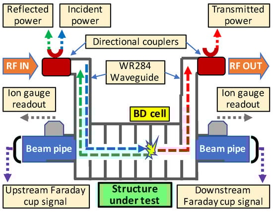
Figure 2.
Layout of the DUT and diagnostic systems. The arrows show the signals read by the acquisition system.
It can be observed that, through the directional couplers located before and after the DUT, a sample of the incident, including both reflected and transmitted RF signals, is extracted. These signals are those which are mixed at 62.5 MHz, sampled at 250 MSPS with AC coupling and later, in the FPGAs, undergo a pre-processing consisting of low-pass digital filtering and digital I-Q demodulation, from which the amplitude and the phase of the signals are obtained at a clock rate of 250 MHz. These amplitude and phase samples are stored in the internal SRAM memory of the Virtex-5 SX501 FPGA of the NI FlexRIO 7961R module and, before the next RF pulse arrives, these data will be sent by PCI express to the “CPU Board”. The PCIe buses are used for both the transmission of pre-processed data from the different acquisition cards to the CPU card and for sending the configuration and monitoring data between the CPU and the rest of the modules. Figure 3 shows a screenshot of the front-end LabVIEW panel with the amplitude of RF pulses signals readout at the CPU board, after I-Q demodulation and low-pass filtering. It can be observed from Figure 3 and Figure 4 that the time resolution of the acquired amplitude and phase signals are rather high; they are, in fact, the signals coming from the ADC, which for a 250 MSPS ADC yields a resolution of 4 ns. The procedure is explained in [12] and will be further detailed in Section 2.6.
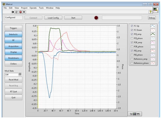
Figure 3.
Screenshot of the RF signals on the LabVIEW front-end control panel.
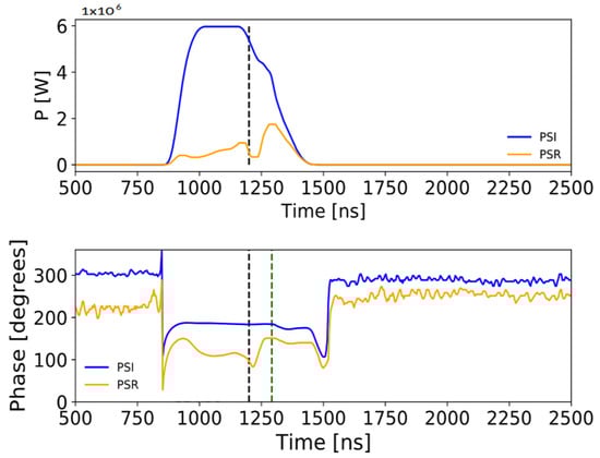
Figure 4.
Power structure incident (PSI, blue) and power structure reflected (PSR, orange) pulse amplitudes (top plot) and phase (bottom plot) signals obtained after offline processing. The trigger of the breakdown is indicated with a black dash line and the maximum of reflected power with a green dashed line, which are the time instants that will be used for reflectometry analysis.
Within the FPGA, the information relating to the amplitude is used to check, pulse by pulse, if it exceeds certain thresholds and, thus, decide if there is a breakdown, in which case it is signaled to the “Trigger + interlock card” through one of the dedicated lines for backplane triggers and/or the interlock PXI. The amplitude and phase data will be used offline to perform reflectometry analysis and obtain the position of the breakdown. For this analysis, the time differences between the transmitted and reflected signals and the incident and reflected signals, respectively, as well as the information on the phases of the signals, will be used. Figure 4 shows an example of the signals used offline for breakdown data analysis.
With the same RF signals, which also pass through the logarithmic amplifiers, and with the signals from the Faraday cups (which are represented with dotted purple arrows in Figure 2), the processing is easier in other modules since they are read directly coupled in DC. It is then checked within the FPGA whether they exceed a certain threshold to indicate if there is a breakdown.
Regarding the algorithm implemented in the “CPU Board”, it is focused on the testing of cavities and its conditioning process. The RF conditioning process follows that of CERN’s Xbox-3, as described in [13]. The algorithm has two levels of hierarchy. The first is a timing cycle, which increases, maintains or decreases power by a user-defined amount depending on the short-term behavior of the structure (typically 2–10 min). This allows power to be increased smoothly by tens of kilowatts every few minutes, instead of the multiple-megawatt jumps every few hours/days typical of a manual mode of operation. The second part of the algorithm observes the evolution of the breakdown rate on a longer time scale (1 million RF pulses) and prevents the increase in energy if this rate exceeds a value defined by the user, typically around 3 × 10⁻⁵. The resulting behavior is a constant increase in power in which the breakdown rate remains constant around the defined value.
In order to control the power injected to the structure, a PID is used within the control loop which compares the incident power with that defined by the conditioning algorithm. The power in the structure is calculated from the incident RF signal already mentioned above and from the calibration measurements made previously in the entire RF chain, from the DUT to the ADCs, which are adjusted to a given second-order equation according to the relationship between the power and the voltage, which is ultimately what ADCs acquire. It should also be mentioned that every time a breakdown occurs, the RF power delivery to the structure is restarted from zero, and the PID is in charge of matching it to that indicated by the algorithm. This process lasts a few seconds, as seen in Figure 5. Based on our expertise, this is the most reliable and safe way to carry out the conditioning.
Figure 5.
Example of how the PID control system increases the power until it equals that requested by the conditioning algorithm after the production of breakdowns.
2.4. Proposal for a New System Based on μTCA Architecture and Open Source Standards
This contribution describes the development of a control system similar to the one already implemented on the PXI system, but based on the μTCA standard, particularly on specification 4. It also proposes to explore the use of open-source software tools for real-time control, including Linux-RT, Linux-CGL and high-level Python programming software.
The essential premises the system must accomplish for the current project are shown schematically in Figure 6 and reflect those described in the previous section: the control system has to be highly configurable to be able to carry out different types of experiments and modify the possible control strategies; RF generation should be enabled; it should be able to acquire reflected and transmitted signals, as well as dark current signals from Faraday cups; it needs to perform real-time pre-processing in FPGA; it should have aggregated high-level real-time CPU processing; it should be able to manage trigger and interlock signals for the whole system; it needs to monitor the pressure level in the structure; and it needs to take readings of environmental signals.
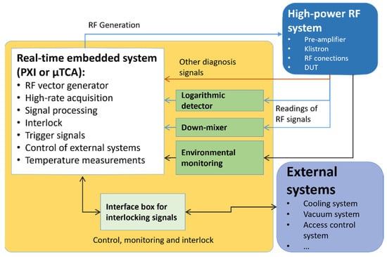
Figure 6.
Proposed LLRF control system essential to operate accelerator cavities.
It is important to highlight that, in the proposed system, the “Down-mixer” element must be specifically designed for both the resonance frequency of the cavity to be tested and the sampling frequency of the ADCs. Currently, a down-mixer is in operation in the laboratory that converts signals from 2.9985 GHz to 62.5 MHz. The proposed project also intendeds to accommodate 750 MHz cavities with an acquisition rate of 125 MSPS; therefore, a new ad hoc multichannel down-mixer is being developed.
2.5. μTCA System Specifications
MicroTCA or μTCA [7] is an open standard developed by PCI Industrial Computer Manufacturers Group (PICMG®) to implement robust computing systems. This organization also manages the Compact PCI®, AdvancedTCA and the Advanced Mezanine Card (AdvancedMC ™) module standard.
The μTCA specifications were published to establish an open standard, with the main objective of facilitating the reuse of existing concepts, and as a complementary system to the advanced telecommunications computing architecture (ATCA) for the development of applications which require a low commissioning cost, smaller physical size, lower capacity and less stringent requirements compared to an ATCA system. μTCA is an integrated system with a scalable architecture which offers flexibility to build reliable, high-performance systems, mainly for telecommunications networks which always demand high availability. However, due to its modular capacity and processing power, its use is already widespread outside of telecommunications networks. In addition, the μTCA specification 4 adds functionality and capabilities to the standard, some of which are of great interest to accelerator and particle physics acquisition systems. The primary purpose of this specification is the inclusion of rear transition modules (RTMs). The main functions of the RTM are to expand the space for data processing or storage and to extend the front panel of the AMC to provide additional connectivity to the system. To achieve this, it defines new rear connectors on the AMC and space for rear slots on the chassis. These high-speed connectors located on the back of AMCs and RTMs can be used to create multiple interconnections within the system or with the outside world, thus providing a level of versatility that previous μTCA specifications could not achieve. RTMs allow for greater flexibility in signal routing and are typically used as analog front ends to AMCs.
For these reasons, it has been decided to develop the LLRF control system using this standard. The base system is made up of a set of AMC cards which are implemented in a modular structure, within a chassis or crate, and which allows applications to be scalable. The AMCs contain the hardware and software (whose functionality is explained in the next section) which will allow, among other tasks, signal processing and generation, as well as data capture. Adjacent to the AMCs is a μTCA carrier hub (MCH), the main management module, which enables and controls the rest of the μTCA system modules. The MCH is also responsible for data switching between modules through the backplane and for the power control provided by intelligent power management units (PM) and cooling units (CU). Figure 7 shows the component diagram of the system.
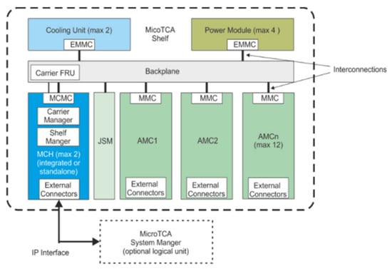
Figure 7.
Block diagram of a μTCA system.
Figure 8 shows the conceptual design of the μTCA system being built, which is similar to that explained in Figure 6. However, in this case, certain specificities related to μTCA architecture and hardware are shown. It can be seen in this diagram, specifically in the “Synthesizer” block, that the central operating frequency is 750 MHz. This frequency is the one used by the vector modulator for up-mixing and for the generation of the RF signal, which goes to the high-power system. In addition, from this same block, the local oscillator signal, which will be used in the down-mixer to obtain the IF signals, the clock signal of the ADC which samples the IF signals and a 10 MHz reference, is generated. This 10 MHz clock is the reference to synchronize the RF signal, the LO signal, and all the acquisition modules of the μTCA system. In order to implement this, the 10 MHz signal is sent to the chassis and redistributed to all the AMC modules through one of its multiple specific lines for transporting clock signals. AMC modules, in turn, are usually designed with enough flexibility to enable embedded FPGAs to operate with both internal and external clock signals. The 10 MHz signal is the clock source, and all the necessary clock signals will be generated from it so that the system as a whole works synchronously. In the case of the IF signal acquisition module, the clock required by the ADC must be provided externally and, therefore, a 125 MHz signal is provided from the “Synthesizer” block. The figure also shows other important elements, such as the trigger signals, which are needed to work in a pulsed manner, the interlock signals, which can come from different equipment, and additional elements labeled as “Beam diagnostics”, which include different types of detectors that can be used to monitor the particle beams that can abandon the cavity, including the aforementioned Faraday cups.
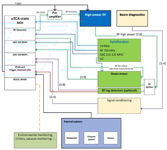
Figure 8.
Global architecture of the LLRF system to be implemented using a μTCA platform.
Figure 9 shows the internal structure of the “Synthesizer” block. The 10 MHz reference source is a high-stability and -precision 10 MHz oscillator module from Pasternack with a phase noise of −150 dBc/Hz at 10 KHz [14]. This clock is distributed to three PLL LMX2592 systems from Texas Instruments that are able to generate signals with a phase noise around −100 dBc/Hz at 10 KHz. The clock is used to produce the 750 MHz RF signal, that of 125 MHz for the ADCs and 718.75 MHz for the LO, so the IF frequency generated is one-fourth of the sampling frequency of 125 MSPS. Two extra 10 MHz outputs are available to synchronize other external equipment.
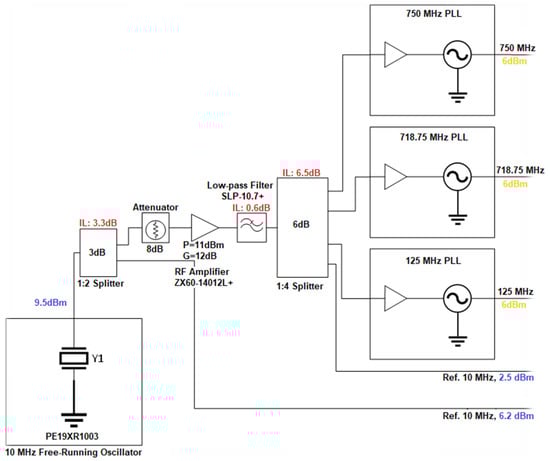
Figure 9.
Internal structure of the synthesizer block. The different components used are shown with their insertion losses (in red), gains and compression point at 1 dB in the case of the amplifier, as well as the nominal output powers (synchronization signals in blue and RF outputs in yellow).
To conclude the description of the most relevant blocks of the system, Figure 10 shows in a simplified way another of the central elements in the RF and synchronization system, the down-mixer. As can be seen, the LO signal is distributed to the different mixers, which are also reached by the external RF signal with a maximum amplitude level of −5 dBm, and from which the IF signal is obtained and subsequently amplified and filtered. In addition to the up to eight RF signals that the down-mixer allows us to mix, an extra reference signal called “RF-REF” is necessary, and which is a direct sample of the 750 MHz signal from the generator, as was also shown in Figure 8. This signal is used as a phase reference in the post-processing of the data, and all the phase measurements of the signals coming from the structure are made with respect to it.
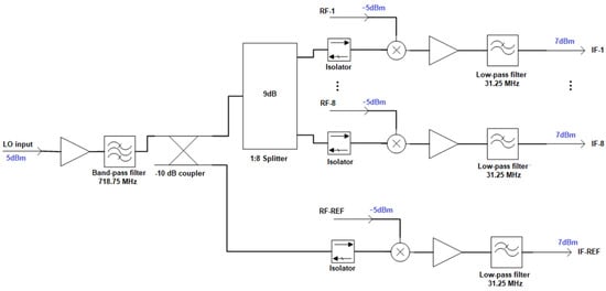
Figure 10.
Simplified diagram of the down-mixer block.
2.6. Control Algorithms in Real Time
Before proceeding to explain the algorithms and functionalities to be implemented by the different elements of the embedded control system, it is necessary to understand the functional distribution of the μTCA chassis to be developed and put into operation, as shown in Figure 11, which does not necessarily match the physical real distribution inside the chassis.
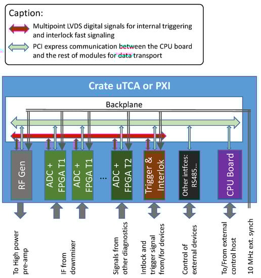
Figure 11.
Conceptual diagram of the embedded modular system with the fundamental elements to carry out the control and acquisition of the LLRF system.
The diagram shows the different input and output sources of data and signals in the system at the chassis level, as well as the different types of modules or cards which make up a typical LLRF system. It can also be seen how the different modules are interconnected with each other through the backplane, both through LVDS multi-point bus digital signals (M-LVDS) and through PCI express (PCIe) data buses. The M-LVDS signals are used for the distribution of the trigger signals between the different cards of the crate and also for the possible internal interlock signals. The PCIe buses are used for both the transmission of pre-processed data from the different acquisition cards to the CPU card and for sending the configuration and monitoring data between the CPU and the rest of the modules. Finally, it is necessary to mention the external 10 MHz synchronization signal, which is distributed between the different modules and used to derive all the clocks that are used in the digital logic of the different FPGAs, ADCs and DACs. This is essential to ensure that the entire RF generation and data acquisition system works synchronously, and that phase control and measurements can be performed on the RF signals.
Next, a brief explanation of the logic and functionality that is executed in each module is provided:
- “Trigger & Interlock”: This module is based on an FPGA in which two different functionalities are implemented. On the one hand, there is the digital logic, which allows the generation of trigger signals in a totally flexible way, and on the other, there is the logic that captures the different interlock signals that arrive through external connectors, or through the backplane, and propagates them to other elements of the system. Both functionalities are executed in parallel and independently within the FPGA. In these modules, the FPGA is synchronized with the rest of the AMC cards through the clock signals TCKLA and TCLKB, which are differential lines of the backplane that are used as input sources for the clock manager modules (MMCM).
As for the trigger signals, they determine the RF pulse rate and must have, as configurable parameters, the pulse rate in a range of 1400 Hz, the pulse width in a range from ns to μs and the delay in the range of tens of nanoseconds to milliseconds. In addition, these trigger signals normally have to be able to synchronize with a 50 Hz signal as well as the power supply network, since the performance of high-power RF equipment, and specifically klystrons, depend on the synchronism with the frequency of the network. This means that the 1400 Hz frequencies have to be generated synchronously as integer multiples or divisors of the 50 Hz frequency.
Regarding the interlock signals, the firmware must allow the different signals to be masked depending on the conditions or operating mode of the different equipment. For example, it could be the case that, due to operation and maintenance tasks, you only want to pulse the klystrons without the need to send RF to the DUT and, therefore, the cooling system of the DUT does not have to be in operation and should not interlock the operation. All the logic implemented in this FPGA can work on a single clock domain, except for the one related to the PCI express interface.
- “ADC + FPGA T1”: These cards are responsible for sampling the IF signals and performing the initial pre-processing of the RF signals which come from the high-power RF system. The IF signals which reach it are used for: the experimental studies of the DUT or accelerator cavity; the closed-loop control of RF power transmitted to the cavity; and the phase control of RF signals, among other uses. The μTCA system includes an AMC card containing the FPGA and a set of ADCs, connected via an LVDS bus.
For sampling the IF signals, the FPGA performs the management and distribution of the clock signals, which are necessary to generate the sampling and trigger signals of the ADCs and make the conversion of the analog signals. Using a software processor implemented in the FPGA, a simple firmware application serves as a user interface with which to control a set of registers to perform the ADC configuration. In addition, the FPGA manages a DMA channel to temporarily store ADC data in DDR-RAM for later processing.
These IF signals are demodulated as I-Q in the FPGA, they are digitally low-pass filtered with a linear phase FIR filter and, subsequently, the amplitude and phase information is extracted from the I-Q samples. From the amplitude information, a first check can be made to test whether the power levels coming from the RF lines are excessive and, in which case, to generate an interlock signal which is transmitted through the backplane to the rest of the system. The sampling frequency of the ADCs on this card are normally high (>100 MSPS) and, since they are RF signals, they are usually AC-coupled. The IF frequency is usually chosen in a way that allows 4 samples per IF signal period (fS = 4·fIF), which simplifies I-Q demodulation (Figure 12) since it yields a phase advance of 90° between two consecutive samples. The digitized samples are directly I, Q, -I, -Q, I, Q, etc., which means that, from any two consecutive samples, the I and Q values of the phasor can be obtained and, therefore, the amplitude and phase components of the IF signal can be extracted with a simple calculation, as shown in Figure 12. By performing this operation at a rate of fS, i.e., with one sample overlap for every two, amplitude and phase information at the ADC sample rate is obtained. These operations must be executed on an FPGA in order to run in real time.
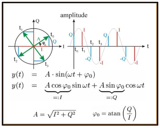
Figure 12.
I-Q demodulation.
The greatest complexity lies in the different clock domains that must be defined, since the reading of the ADCs and the processing cannot operate at the same speed. In current PXI cards, it has been seen that for a data reading frequency of 250 MSPS, the synthesis and routing algorithms fail on multiple occasions when processing the data from 4 reading channels at a frequency of 40 MHz. It is difficult make a clear assessment of the reason for this limitation with the LabVIEW-FPGA tools, but it may be related to the 23-stage FIR filters that are used to remove the harmonics which are missed by the analog filtering.
- “ADC + FPGA T2”: These other cards are like the previous ones, but are used for another purpose, such as reading the signals which come from Faraday cups, from the logarithmic detectors or from the BPMs (beam position monitors). In each case, the sampling rate and the type of coupling (AC or DC) is chosen according to the needs, but it is usually within the range of 100–250 MSPS. The pre-processing in FPGA can also be very varied, from the simple detection of thresholds, as would be performed for the Faraday cup or the logarithmic detectors signals, to non-linear corrections of a higher order, decimated and filtered, as in the case of BPMs.
This is possible since the FPGA includes its own code cores, which are configurable, and which implement the different post-processing algorithms according to the specified parameters. Data capture and access are performed in a similar way to the previous module.
- “RF Gen”: This module is a configurable arbitrary RF signal vector generator. Internally, it is made up of an I-Q modulator, a high-rate DAC (>100 MSPS) and an up-mixer to raise the desired operating frequency. The FPGA allows us to configure an appropriate clock signal for the DAC and send the specific I-Q samples multiplexed for each trigger signal that comes from the “Trigger & Interlock” module. The I-Q samples can be generated both internally in the FPGA (directly or through a DMA channel for access to the DDR-RAM memory), or they can come from the “CPU Board” module through the PCIe bus. Therefore, the FPGA is also in charge of managing the operation of the PCIe port by configuring the MGT modules that facilitate the data transmission to other cards connected to the backplane of the μTCA system.
This last option offers a greater degree of flexibility since it can be implemented at the software level, at the cost of greater data traffic through the backplane and an increase in the computational load and latency of the processes that run in the real-time system of the “CPU Board”.
- “CPU Board”: This module consists of an embedded CPU that has to run an operating system in real time and manage the control of the entire system. This module must perform as a priority and, therefore, must execute the following in strict real time: collect all the data which come from the ADC cards, check the trigger and interlock signals from “Trigger & Interlock”, and perform the closed-loop control (usually one or more PIDs) of the RF power going to the DUT or accelerator structure. In addition, it is also responsible for reading with lower priority the values of ambient temperatures, vacuum levels of the waveguides and DUTs, sending monitoring signals to the user host, etc.
- “Other interfaces”: These modules are usually used to communicate with devices through RS485, RS232 and Canbus protocols.
2.7. CPU Board Algorithms
The current PXI system runs National Instruments’ own real-time operating system on the crate CPU. The programmed code has been made in LabVIEW and its structure responds to Figure 13, and the same scheme is followed in the μTCA system. The code execution sequence consists of an initialization phase and the initial configuration of services and hardware components. Next are the tasks that require real-time processing, which will be executed concurrently and are explained below, and finally, in the case of aborting the system execution, the orderly closing of services.
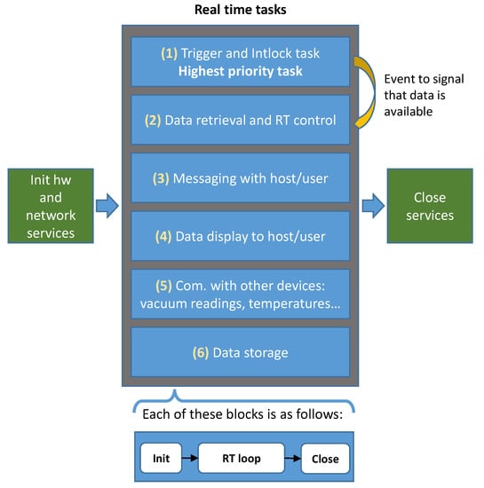
Figure 13.
General structure of the code in the real-time system.
Before describing the content of each task, it is worth highlighting several characteristics of the previous system. The tasks listed from (1) to (6) all respond to the paradigm indicated in the lower part of the figure, in which the hardware is initialized first (ADCs, FPGAs, RS-232 communications, FIFOS, memory space, etc.). Then, a permanent real-time loop is entered and, finally, the resources are freed in the case of aborting the loop. It should also be noted that task (1) is the highest priority, since it is in charge of checking whether there are new data available and, if so, it sends alerts by propagating an event to task (2), which is the one in charge of collecting the data from the ADC modules and performing all the processing in real time.
(1) “Trigger and Interlock”: this is considered to be a critical periodic task, whose execution frequency is within the 1 MHz range and must present very low jitter. The main function consists of reading through the PCIe bus the status of the “Trigger and Intlock” card and checking if a trigger signal has been generated for the acquisition of new data. If so, an event will be propagated for task (2) to read the data. Ideally, this task should run in a parallel thread or process in order to have a different processor core assigned from the other tasks.
(2) “Real-time data reading and control”: this is a critical sporadic task, triggered by an event in task (1). Its main function is to read through the PCIe bus the data pre-processed by all the ADC cards and store them in a FIFO stack or in shared memory, depending on the application. These data will then be used to perform the necessary processing for the closed-loop control of the system. In the current application, multiple PIDs are running in parallel. In a simple way, one of the PIDs is in charge of keeping the set RF power in the accelerator structure, for which it needs to read the amplitude and phase of all the incident and reflected RF signals periodically. Another PID is in charge of performing the long-term conditioning of the cavity, for which it has to continuously calculate the breakdown rate and, depending on whether it is below or above a critical limit during a given period of time, increase or reduce the setpoint RF power. In this task, determinism is essential and will depend on the trigger rate, which, in the current system, is stipulated as a maximum of 400 Hz, which gives a time limit of 2.5 ms in the most critical case. To handle this in LabVIEW, the threading and, therefore, the capability to assign tasks to specific cores is implemented in the real-time module. In this module, there is a loop structure, called “Timed Loop”, which has the capability to execute one or more subdiagrams of code sequentially on each iteration of the loop at the specified period, i.e., they can be used to execute deterministic code. This code is executed in a single system thread and can be assigned manually to a dedicated CPU or core in order to reduce jitter. In other open platforms, as introduced in the next section, the way to handle this critical task is to implement parallel processing in a real-time Linux operating system with the process scheduling assigned to a specific processor.
(3) “Messaging with host/user”: this task is in charge of managing the exchange of messages and configuration data between the crate and a remote user. This exchange can be both synchronous and asynchronous, depending on the importance of the information transmitted. As a general rule, it can be specified that the control and configuration commands must be synchronous, while other information, such as temperature values, vacuum levels, etc., whose update is periodic and not critical, can be asynchronous. This task can be considered to be uncritical or interactive.
(4) “Visualization of data towards the host/user”: this consists of the transmission of samples of the data read from the ADCs so that the remote user can make a visual presentation of the RF signals of the structure. It is considered a transmission method where packet loss is not relevant. This task is considered to be uncritical.
(5) “Communication with other devices”: this task or set of tasks is in charge of controlling and monitoring other devices of the system through communication protocols, such as Ethernet, ModBus, CanBus, RS-485, etc., and publishing the data and/or putting them at the disposal of other tasks, such as control (2). This task is uncritical.
(6) “Data storage”: all data pre-processed, processed and acquired through other devices must be stored in some type of database or storage file, whether local or remote, under the premise that the information stored keeps a pulse-to-pulse timestamp. This task is uncritical.
2.8. Development Plans Based on Open Standards
As discussed in Section 2.4, emerging industry standards, such as AdvancedTCA, MicroTCA or Carrier Grade Linux, among others, make possible the implementation and development of a new category of communication servers through the use of open standards and tools for use in embedded systems that can deal with a wide range of specific applications beyond the telecommunications spectrum, such as within the scientific field, for the monitoring and control of instruments that distribute a large amount of information such as the LLRF system that is described in this article.
The development at the firmware and software level that will make up the main application of the system, and which will be executed within the communications server itself in its internal CPU module, should also be based on open-source tools to reduce third-party dependencies and licensing costs. Along with this, it is of interest that certain standards and restrictions are also met for the correct execution of the applications. Some of the criteria adopted for their fulfillment are described below.
The μTCA standard implemented is intended for small developments that meet, among others, the “Carrier Grade” or CG specification, and it is, therefore, desirable that the software development also complies with them. In these types of systems, carrier grade refers to either a hardware or software component which is extremely reliable, is well tested and verified in its capabilities. CG systems are tested and designed to meet or exceed high availability definitions, and provide very fast failure recovery through redundancy.
Based on this specification, it has been chosen to use an open operating system that complies with this specification, and which avoids the use and dependence of proprietary systems, in order to reduce costs and improve adaptability. It has been decided to develop the system using a Linux OS that complies with the CG specification, known as “Carrier Grade Linux” or CGL. CGL is a set of specifications detailing the standards for availability, scalability, manageability and service response characteristics which must be met for the Linux kernel-based operating system to be considered to be carrier grade [15].
The Linux Foundation CGL workgroup of the Linux Foundation have released version 5.0 of their Carrier Grade Linux (CGL) specification for operators. This version introduces updates which increase security and reliability, for example in file systems, and aims to provide a platform for a market in which the demands for transferring data between networks have increased [16]. This project uses tools for the development of a Linux operating system which adapts to this version of the specification.
Currently there are various CGL distributions, among which MontaVista and WindRiver or Yocto [17] stand out. These distributions provide a flexible set of tools and configurations which can be used to create customized and optimized Linux distributions for embedded devices and IOT on any architecture, and they have been analyzed for the next generation of custom Linux distribution, which will act as the main OS of the system. After a comparison, the distribution finally chosen was WindRiver, which was developed from the Yocto project, and which makes a wide set of tools available to developers and offers free support within their plans and products for clients. Its main advantage over others is its considerable ease of ease when it comes to the implementation and configuration of a CGL distro on different platforms.
Given this, the implemented operating system distribution meets the initial objectives proposed in terms of being developed from open software and meeting the CG specifications. However, given the nature of the application designed to act on the designed μTCA system, it is truly necessary to use an RTOS or real-time operating system, which will be used to execute individual processes or algorithms in real time, as described in the previous chapters. This RTOS must be set up to provide a predictable execution pattern and must be within time constraints, that is, the processing completes with a certain latency, or the system as a whole could fail.
The decision to use an RTOS is due to its ability to have an advanced algorithm for scheduling tasks. As described, the key factors in a real-time operating system are minimal interrupt latency and minimal inter-process switching latency. For this system, the speed or predictability with which it can respond to events will be more valued than the amount of work it can perform in a given cycle of time, which is how GPOS or traditional operating systems work.
The Linux operating system itself is not capable of working strictly in real time. Therefore, from our generated CGL distribution, it is necessary to patch its kernel with an additional PREEMPT_RT patch, in order to offer RT support and obtain real-time capabilities [18]. This modification will be made using WindRiver’s own configuration tools, indicating in them how the sources should be downloaded and patched. Later, the new kernel configuration must be adapted. Afterwards, the kernel can be compiled again and started, verifying its new functionality.
For the FPGA firmware development, the Vivado tool has been employed during the first stages of the system development. The FPGAs used belong to the Kintex-7 family from Xilinx, and the use of its proprietary design and synthesis tool simplifies the design and commissioning of the first performance tests.
It has been decided to test the free tool HDLmake in parallel with Vivado as an aid in the management of the created HDL projects. This open-source tool generates automation files (makefiles) which contain the commands to generate the projects and allows other known tools (Icarus Verilog, Ghdl, modelsim, Altera Quartus, Xilinx Vivado, ISE, etc.) to execute the simulation, compilation, or bitstream generation. The configuration is implemented using the Manifest.py files in which the source files of the design, the simulation files (testbench) and the tools to be used are indicated. The main reason for using this tool is its modularity, scalability and capability to reuse sources, in addition to the ability to download codes from remote repositories.
Regarding the HDL description language, both VHDL and Verilog are used, as some third-party cores are being utilized and they are developed in either language. This is another reason to explore the use of other open-source tools for the compilation of these modules, such as Icarus Verilog or GHDL. Both tools allow the compilation of codes defined in these languages, and which can later be simulated in order to verify their proper operation.
Finally, within this set of criteria applied in software development, it is convenient to implement the functions of the algorithms using a programming language for real-time systems. In general, a real-time operating system can guarantee that the tasks it handles are deterministic, but the operating system may not guarantee that the developer’s software code runs equally in real time. Fortunately, there are several languages of interest for real-time programming, such as C/C++, ADA or even JAVA. However, initially for this development, we want to explore the use of a high-level language such as MicroPython for the development of the source code which will form the critical applications of the system mentioned above.
MicroPython is a simple and efficient implementation of the Python programming language that is optimized to run on microcontrollers and in restricted environments. According to the content of the reference [19], several strategies and tactics are necessary to solve the latency problems due to the use of this interpreter; however, there are many known benefits of using Python for the development of RT applications, including the benefits of developing and debugging more easily or generating simpler and more understandable code. Among our future objectives, we need to carry out a test bench to quantify the response in the execution time of the applications on the RTOS system. Therefore, the algorithms are programmed using the RT language. Each algorithm represents a specific task (see Figure 13) and is executed inside a process. Some of these processes require execution in parallel with respect to other processes (which execute low-priority tasks) to achieve greater efficiency. For this reason, they have a processor core assigned exclusively to them in order to avoid competing for the core resources, thus obtaining the best possible performance and also guaranteeing an optimal parallelism. To meet this objective, the Gnu/Linux taskset tool will be used to indicate to the OS task scheduler which core can execute these processes. This tool modifies the affinity flag (AF), a bit mask which represents each available processor, and which is created for each new process, forcing it to run on a specific core or dedicating a core only to a particular process. Once configured, the Linux operating system scheduler will not assign any regular processes to the reserved kernel.
3. Results
The μTCA system architecture is totally defined and its real implementation is ongoing. The technicalities between PXI and μTCA are different, and a complete and detailed performance comparison is not available at this point. However, it is worth showing some partial results to demonstrate the feasibility of this open standards approach using μTCA.
Figure 14 left shows a pulsed RF signal coming from the RF generator module (see also Figure 11) used to feed the high-power pre-amplifier. It is a pulsed signal with a central frequency of 750 MHz and a configurable repetition frequency between 100 Hz and 400 Hz. In Figure 15, some periods of the IF signal corresponding to the down-mixed RF (750 MHz) are shown. In this case, an LO frequency of 718.75 MHz has been used in order to obtain the 31.25 MHz IF, which is sampled by the 125 MSPS ADCs and yields four samples per period (marked with red lines in the figure), as needed for the quick I-Q demodulation. This sampling is completely synchronous, so the sampling phase is repeatable in every period, as can be seen in the figure. This is an essential requirement to properly recover the amplitude and phase in the digital I-Q demodulation.
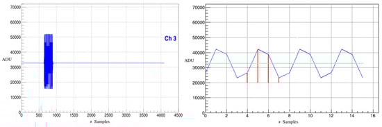
Figure 14.
Generated pulsed RF signal centered at 750 MHz (left plot) and sampled IF signal at 125 MSPS (right plot).
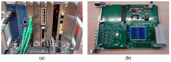
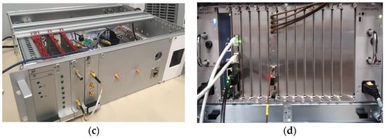
Figure 15.
Hardware employed in the LLRF system. (a) Mini-µTCA crate for system development. (b) Self-made multipurpose AMC card. (c) Frequency synthesizer to generate the LO and synchronization signals. (d) Final full-size µTCA crate to be used in the facility.
Finally, in Figure 15, some pictures of the hardware employed to build the LLRF system are shown. The top-left picture shows the mini-µTCA crate used to test the self-made AMC cards without compromising the integrity of the real system and carry out the development work. In this image, different modules of the µTCA system as described in the block diagram in Figure 11 can be seen. From left to right: the power module (leftmost); the MCH; the CPU module; the “trigger and interlock” AMC card with an FMC mezzanine card to sample external signals; the “RF Gen” module and “ADCs + FPGA” from the manufacturer Strück in the same slot, since it is implemented as a µTCA frontal and real transition module. The top-right picture shows the self-made AMC card with the FMC ADC module used for the sampling of control analog signals as well as for “trigger and interlock”. The bottom-left picture shows the frequency synthesizer designed to provide the LO and synchronous signals needed for the system. Finally, the bottom-right picture shows the full-size µTCA crate, which hosts the complete system.
4. Discussion
Based on the experience gained in the development and implementation of the current LLRF system of the laboratory, on the results obtained by other research groups in the development of LLRF systems with μTCA, and based also on the preliminary results obtained by us so far with the same platform, implementing a system similar to PXI is feasible. The same external RF hardware and electronics interfaces which are currently working at the facility are in use, and they have already been tested and are working properly. The new RF synthesizer and mixer of 750 MHz have already been built and characterized with specific RF instruments (spectrum analyzer and VNA), following the same experience as for the previous S-Band system [1]. Hereafter, there follows a brief description of the development and deployment strategy for the μTCA system.
The commissioning procedure of the whole system is a long and complex task. Once all the external hardware pieces are working, an approach from least to most complex is followed. Therefore, the first step is to start by autonomously commissioning a prototype μTCA system with the vector modulator and the acquisition system working in a synchronous manner. This is achieved by feeding back the output of the modulator vector to the ADCs with a directional coupler and checking that it is possible to acquire the data from the modulator vector synchronously, as it has been already implemented. The next step is to add the VHDL code to perform the I-Q demodulation and to store the amplitude and phase results in the internal memory of the FPGA, so it can be fully read out by means of some software tool. After this, the I-Q vector modulator needs to be calibrated, since these devices always show I-Q imbalances which need to be corrected [20]. This error correction is completed at software level and consists of a series of correction factors applied to the I-Q samples, which are sent to the modulator vector so that the RF output is as exact as possible. The calibration of the ADCs inputs with respect to the RF input power in dBms scale can also be performed at this stage, although it is not completely necessary, However, both calibrations must be performed at some point before operating with the real signals and a real DUT.
After this point comes the commissioning phase of the “Trigger & Tnterlock” AMC board. Once the modulator generator, RF acquisition and triggering and interlocking cards are working together with a basic functionality, it is time to move on to the commissioning of the real-time system in the CPU. This requires a long, iterative development process in which the different tasks of the real-time system are implemented one after the other. These will monitor, read and reconfigure in real-time the other μTCA system boards. Once this basic core consisting of the CPU real-time system, the “trigger & interlock”, vector modulator and acquisition cards are working coherently, it is possible to proceed to add extra functionalities or to rescale the system to a larger number of generator or acquisition cards. Among the extra, but essential, functionalities are the software user interface, additional high-speed boards to acquire the signals from beam diagnostic detectors, slow acquisition boards to monitor the status of high vacuum pumps, RS485 interfaces, etc.
Once the system with the basic functionality briefly described above is running, one can begin the integration phase with the high-power RF system. This phase is highly dependent on the facility characteristics, but it is usually a high-priority task to make sure that the interlock interface between the high-power, vacuum or other safety equipment with the μTCA system works safely and reliably. This is critical because applying high RF power to a system that is signaling an interlock (and thus should not be operated), can permanently damage valuable equipment. When the RF can finally be driven to the high-power equipment, then a phase in which the triggering of the different devices needs to be synchronized can begin. It is of utmost importance that the FPGA code that implements the trigger dispatching is flexible enough to allow trigger signals with different delays, since not all devices have the same operational latencies. At the same time, it is necessary to ensure that the RF power reaching the ADC inputs is within a suitable range, so that they are strong enough to be above the noise floor, and not too high so as not to damage the devices.
5. Conclusions
During the development of this project, it has been possible to verify that it is feasible to design a platform with benefits similar to the current one, located in the IFIC laboratory, using only open architecture standards at both hardware and software levels. The μTCA system thus developed behaves similarly to the PXI in terms of scalability and flexibility, but with the advantages of having a lower cost than similar systems, as well as offering reusability and compatibility with existing technologies. Likewise, the benefits of developing software with free tools allow us to reduce licensing costs and install them on any number of devices, as their use is not limited, along with the possibility of modifying their source codes according to our needs. Compliance with the CGL standards and the use of RTOS utilities allow us to guarantee the service response objectives that must be met with respect to having high reliability and providing recovery from failures, as well as the requirements in the limitations of latency times for the execution of the applications.
Regarding the difficulties encountered, μTCA is a relatively new standard compared to other similar existing ones. The documentation, even though it is abundant, is very generic, which makes it necessary to consult with module manufacturers to carry out certain implementations. It is necessary to program both the hardware and software of the modules together with a correct configuration of the MCH to establish the communication channel in an optimal way, in our case through a PCI express. At the level of software programming, it is also necessary to develop a driver for access to the PCIe so that data transfers between modules are transparent for the main application.
Author Contributions
Conceptualization, D.E. and B.G.; Data curation, R.M. and J.M.; Formal analysis, J.P.-S. and R.M.; Funding acquisition, B.G.; Investigation, A.M., R.G.-O., J.T., J.P.-S., J.M. and J.S.; Methodology, D.E., R.G.-O. and J.T.; Project administration, D.E. and B.G.; Resources, J.T., R.M. and J.S.; Software, A.M.; Supervision, D.E., R.G.-O. and B.G.; Validation, A.M.; Writing—original draft, A.M., D.E. and R.G.-O.; Writing—review & editing, J.T., J.P.-S., R.M., B.G., J.M. and J.S. All authors have read and agreed to the published version of the manuscript.
Funding
The work presented here has received funding from the Agencia Valenciana de Innovación (AVI) through the DosLINC6+ project with file number INNEST/2020/123.
Conflicts of Interest
The authors declare no conflict of interest.
References
- Esperante, D.; Blanch, C.; Boronat, M.; Fuster, J.; Iglesias, D.G.; Vnuchenko, A.; Gimeno, B.; Lasheras, N.C.; McMonagle, G.; Syratchev, I.; et al. Construction and Commissioning of the S-Band High-Gradient RF Laboratory at IFIC. J. Phys. Conf. Ser. 2018, 1067, 082024. [Google Scholar] [CrossRef] [Green Version]
- Lasheras, N.C.; McMonagle, G.; Syratchev, I.; Wuensch, W.; Golfe, A.F.; Argyropoulos, T.; Blanch, C.; Esperante, D.; Giner, J.; Vnuchenko, A.; et al. Design and construction of a high-gradient S-Band RF laboratory at IFIC-Valencia. In Proceedings of the IPAC2017, Copenhagen, Denmark, 14–19 May 2017. [Google Scholar]
- Clic Detector & Physics Collaboration. Available online: https://clicdp.web.cern.ch/ (accessed on 31 December 2021).
- Baudrenghien, P.; Hagmann, G.; Molendijk, J.C.; Olsen, R.; Rohlev, T.; Rossi, V.; Stellfeld, D.; Valuch, D.; Wehrle, U. The LHC low level RF. In Proceedings of the 10th European Particle Accelerator Conference, Edinburgh, UK, 26–30 June 2006; p. 1471. [Google Scholar]
- Salom, A.; Perez, F. Digital LLRF for ALBA storage ring. In Proceedings of the 11th European Particle Accelerator Conference, EPAC08, Genoa, Italy, 23–27 June 2008. [Google Scholar]
- Butler, T.A.; Allen, L.J.; Branlard, J.; Chase, B.; Paul, W.; Joireman, E.C.; Kucera, M.; Tupikov, V.; Varghese, P. New LLRF system for Fermilab 201.25 MHz Linac. In Proceedings of the LINAC08, Victoria, BC, Canada, 29 September–3 October 2008. [Google Scholar]
- MicroTCA Overview. Available online: https://www.picmg.org/openstandards/microtca (accessed on 31 December 2021).
- Omet, M.; Ayvazyan, V.; Branlard, J.; Butkowski, L.; Cichalewski, W.; Czuba, K.; Grecki, M.; Hoffmann, M.; Ludwig, F.; Makowski, D.; et al. Operation experiences with the microTCA.4–based LLRF control system at FLASH. In Proceedings of the 6th International Particle Accelerator Conference IPAC’15, Richmond, VA, USA, 3–8 May 2015. [Google Scholar]
- Vnuchenko, A. High-Gradient Issues in S-Band RF Acceleration Structure for Hadrontherapy Accelerators and Radio Frequency Quadrupoles. Ph.D. Thesis, University of Valencia, Valencia, Spain, 2020. [Google Scholar]
- Catalán Lasheras, N.; Argyropoulos, T.; Esperante Pereira, D.; Eymin, C.; Giner Navarro, J.; McMonagle, G.; Rey, S.; Solodko, A.; Syratchev, I.; Volpi, M.; et al. Commissioning of XBox3: A very high-capacity X-band RF test stand. In Proceedings of the LINAC2016, East Lansing, MI, USA, 25–30 September 2016. [Google Scholar]
- Bress, T.J. Effective LabVIEW Programming; NTS Press: Austin, TX, USA, 2013; ISBN 1-934891-08-8. [Google Scholar]
- Schilcher, T. RF applications in digital signal processing. In Proceedings of the CAS—CERN Accelerator School: Digital Signal Processing, Sigtuna, Sweden, 31 May–9 June 2007; pp. 249–283. [Google Scholar] [CrossRef]
- Wuensch, W.; Lasheras, N.C.; Degiovanni, A.; Döbert, S.; Farabolini, W.; Kovermann, J.; McMonagle, G.; Rey, S.; Syratchev, I.; Tagg, J.; et al. Experience Operating an X-Band High-Power Test Stand at CERN. In Proceedings of the 5th International Particle Accelerator Conference, Dresden, Germany, 15–20 June 2014. [Google Scholar]
- Pasternack PE19XR1003 10 MHz, Free Running Oscillator. Available online: https://www.pasternack.com/images/ProductPDF/PE19XR1003.pdf (accessed on 25 February 2020).
- Carrier Grade Linux. Available online: https://wiki.linuxfoundation.org/cgl/start (accessed on 31 December 2021).
- Carrier Grade Linux Requirements Definition. Available online: https://www.linuxfoundation.org/sites/main/files/CGL_5.0_Specification.pdf (accessed on 31 December 2021).
- Carrier Grade Linux Registered Distributions. Available online: https://wiki.linuxfoundation.org/cgl/registered-distributions (accessed on 31 December 2021).
- Kodi, S.; Jog, C.H. Testing Real-Time Linux, What to Test and How; IBM Linux Technology Center: Armonk, NY, USA, 2008. [Google Scholar]
- Mahmoud Almostafa, R.; Nabila, R.; Hicham, B.; Mounir, R. Python in Real Time Application For Mobile Robot. In Proceedings of the Smart Application and Data Analysis for Smart Cities (SADASC’18), Casablanca, Morocco, 27–28 February 2018. [Google Scholar]
- Sabah, S.; Lorenz, R. Design and calibration of IQ-Mixers. In Proceedings of the 6th European Particle Accelerator Conference, EPAC’98, Stockholm, Sweden, 22–26 June 1998. [Google Scholar]
Publisher’s Note: MDPI stays neutral with regard to jurisdictional claims in published maps and institutional affiliations. |
© 2022 by the authors. Licensee MDPI, Basel, Switzerland. This article is an open access article distributed under the terms and conditions of the Creative Commons Attribution (CC BY) license (https://creativecommons.org/licenses/by/4.0/).