1. Introduction
The computer science and telecommunication communities have devoted great efforts toward the design of energy-efficient solutions for data transmission and network management. A novel energy-efficient strategy is presented in [
1] for Ethernet networks. Ethernet is used in many fields ranging from industry [
2] to home automation [
3]. The amount of data circulating in Ethernet networks has drastically increased due to the growing number of connections among users, the sharing of multimedia data, and the widespread distribution of devices [
4]. Ethernet technology has been adopted for use in computer communication systems [
5]. For instance, an Ethernet interface can be implemented on a digital signal processor (DSP), such as TMS320F2812, and a controller chip, such as KSZ8851, can analyze the functionality of software in the DSP and in transceiver drivers of KSZ8851. Such functionality can be easily achieved in most embedded systems and can be used in many Ethernet communication applications [
6]. The ASIC design resolves the energy-efficient problem for data transceiver and network management.
Universal serial bus (USB) is also a commonly used communication interface. USB communication data class (CDC) defines Ethernet application over USB protocol, which can be implemented by emulation protocol software. However, CDC exhibits performance degradation, especially when handling small-size and latency-critical data in practical applications. Data throughput gain with low resource utilization was achieved using parallel processing and jumbo frame techniques [
7]. Currently, USB 3.0 is the most popular communication interface for commonly used devices. The transformation of packets from Ethernet protocol to other communication interfaces and protocols is a critical step for connecting different platforms. When embedded devices are connected by a USB bus, it is convenient to use an Ethernet emulation model, which can also be used for conventional TCP/IP networks.
Traditional server-side Modbus transmission control protocols (Modbus TCP) include many unnecessary blocking input–output operations. Some improvements, such as asynchronous nonblocking and multithreading, are applied to the TCP network layer. In [
8], a customized TCP packet format was used to perform Modbus TCP functions and a new method was established to achieve efficient and real-time dialogue between the master and slave. Such methods improve the performance of Modbus TCP and reduce power dissipation. USB Communication Data Class (CDC) defines Ethernet over USB protocol which can be implemented by emulation protocol software. However, it presents a performance degradation problem within a real system, especially for the critical data with small latency. In [
9], two methods based on packet network traffic measurement are studied by simple sniffers and the transformation of captured packet traffic into data source statistics. The TCP/IP protocol stack and fragmentation/defragmentation procedures are considered according to RFC 793. Moreover, the actual Modbus IoT sensors are connected to the 4G/3G/2G router via Modbus TCP Ethernet protocol to server. In general, the 4G/3G/2G router comes with additional storage capacity to develop custom applications [
10]. In [
11], an application software is developed with development board for IoT gateways, including two functions of Modbus over TCP and Modbus to MQTT. It is convenient for controlling the gateway, integrating with apps, and using the AI computing. A greater effort can be made to complete a remote access to the laboratory on industrial communications on popular protocols, such as USB, Modbus TCP, and CAN bus [
12].
Figure 1 shows a neural network direct torque control (NNDTC) architecture for AC induction motor, which is composed of the Hall sensor, successive-approximation register (SAR) analogue-to-digital converter (ADC), rotor speed encoder, and neural network DTC ASIC. By integrating the above-mentioned NNDTC with USB/Ethernet bridge, a mixed-signal IC is completed to control the AC induction motor remotely. The result of this study not only controls the AC motor remotely through USB/Ethernet interface but also stores those controlled codes into PC through the Ethernet/SONET media transport layer. Note that a high-speed bridge is necessary to have a high transmission speed and to relax the bandwidth requirement for different applications.
The introduction of new telecommunication services also requires the transformation of packet histograms into data source statistics. In most cases, the length of the transmitted data is longer than that of the packages. The data source and packet traffic must be connected by fragmentation and defragmentation processes [
9,
13], which can be realized through dual-port static random access memories (SRAMs) (Dual-Port SRAM_1 and Dual-Port SRAM_2). Two SRAMs are used to improve the frequency incompatibility between Ethernet (125 MHz) [
14] and USB (100 MHz) [
15]. The remainder of this paper is organized as follows. The system architecture of the Ethernet and USB 3.0 interface is presented in
Section 2.
Section 3 presents the simulation results.
Section 4 presents the verification of the proposed packet transformation and transmission interface developed using an FPGA development kit.
Section 5 presents conclusions.
2. Bridge Architecture between Modbus TCP and USB 3.0
Figure 2 shows the architecture diagram of the proposed transformation and transmission interface between Modbus TCP and USB 3.0. It is composed of the Ethernet module, two dual-port SRAMs (Dual-Port SRAM_1 and Dual-Port SRAM_2), and a USB module. The Ethernet module is serviced with address resolution protocol (ARP) and Modbus RTU (Remote Terminal Unit) message with TCP, aka Modbus TCP. The Ethernet module receives Ethernet packets from the Ethernet port physical layer (PHY) and sends them to the USB module. Simultaneously, the Ethernet module receives USB data from the USB module and converts it into an Ethernet packet. As shown in
Figure 2, the Ethernet module includes a gigabit medium independent interface (GMII) module, a ModbusTCP_to_USB module, a MAC_send module, a USB_to_ModbusTCP module, and an ARP_send module.
When the Ethernet module wants to send the Ethernet packet to the external device via Ethernet PHY, it needs to send a Request packet to inquire the MAC address of the external device. Next, the external device sends a Reply packet to the submodule MAC_send_module in the Ethernet module. The MAC address of the external device is sent to the submodule of MAC_send_module. Then the transmission of MAC address is completed between Ethernet module and external device.
The GMII module is responsible for transmitting the Ethernet packet via the Ethernet PHY chip using the GMII interface. An Ethernet receiver submodule is responsible for receiving and analyzing the Ethernet packets. If the received Ethernet packet is a correct Modbus TCP packet, it will be stored in Dual-Port SRAM_2. If the received packet is a correct Ethernet ARP request packet, an ARP reply packet is returned to the GMII interface through the Ethernet MAC_send module and the Ethernet ARP_send module. The packet will be discarded if it is incorrect.
The MAC_send module of Ethernet module is responsible for processing the preamble, MAC address, Ethernet type, and frame check sequence (FCS) of the received Ethernet packet. The Ethernet Modbus/TCP module is responsible for processing the IP, TCP, and Modbus/TCP headers and for reading the data stored in Dual-Port SRAM_1. The Ethernet ARP_send module is responsible for processing the ARP header. Two dual-port SRAMs, which are provided by ARM and made using a 0.18-μm CMOS process, have a 128 memory words and a 32-bit word size. When the proposed SRAM is implemented with an FPGA development kit, the two dual-port SRAMs can achieve a 2048 memory words and a 32-bit word size.
Figure 3 shows the architecture diagram of the dual-port SRAMs.
Figure 4 presents the designed USB module based on the specification of CYUSB301X/CYUSB201X [
15]. CLK_100 is a 100-MHz input clock signal. PCLK is the reversed output clock signal of CLK_100. Flag_a and Flag_b are input status signals and are preset to low (0). When the input status signals are high (1), the module is ready to receive data. Flag_c and Flag_d are input status signals and are preset to low. When the input status signals are high, the module is ready to transmit data. The value of SLOE controls data input and output. The USB module receives data when SLOE is high and transmits data if SLOE is low. SLRD is a read enable switch. When SLRD is low, data can be read. SLWR is a write enable switch. When SLWR is low, data can be written. Addr[1:0] is the address for selecting output or input data. Addr[1:0] = 0 is the address for output data, while Addr[1:0] = 1 is the address for input data. DQ[31:0] is a 32-bit bidirectional data transmission port.
Figure 5 presents the flowchart of the Request packet transmitted from the submodule ARP_send_module to external device to obtain the MAC address. First, the ARP signal will be triggered by setting high (1), the MAC address of destination will be set to unknown (48′hffffffffffff) and the Ethernet_Type is set to ARP_type. Next, both ARP and Ethernet packets are transmitted. In the ARP packet, it includes ARP_header, ARP_opcode, Source MAC address, Source IP, Destination MAC address, and Destination IP. Regarding the Ethernet packet, it is composed of Preample, Destination MAC address, Source MAC address, Ethernet type, Payload, CRC (Cyclic Redundancy Check), and Calculated FCS. Then a completed ARP Request packet is transmitted from ARP_send_module to the external device via Ethernet PHY. Conversely, the external device will send a Reply packet to the submodule MAC_send_module by setting the Reply trigger signal ARP_ack_TX to high (1). Thus, the destination MAC address will be replaced by the MAC address of external device.
Figure 6 presents a flowchart of the process of receiving an Ethernet packet and converting it into a USB interface format. First of all, the receiver of Ethernet module is idling and waiting to receive the Ethernet packet. That is, the driving signal of receiver (Rx_dv) is set to high (1) and the error signal is low (0). If the preamble of received Ethernet packet is correct, the FCS calculation is started, and the current state is replaced with the header of the Ethernet packet. After the validity of the MAC address has been confirmed, the protocol type of Ethernet packet needs to be distinguished. If the protocol type is ARP, the received Ethernet packet is resolved into an ARP packet (A). Otherwise, the received Ethernet packet is resolved into a Modbus/TCP packet (B). Note that the Ethernet packet is discarded if an error is found in the receiving process.
Figure 7 presents a flowchart of the process of receiving an ARP packet in the Ethernet module. First, ARP request and reply packets are distinguished. If the packet is an ARP request packet and the packet format is correct, an ARP reply signal (ARP_ack_TX) is set to high (1) and sent it to the Ethernet PHY (Request device). If the packet is an ARP reply packet and the packet format is correct, the destination MAC address is received and stored in the register.
Figure 8 presents a flowchart of the process of receiving a Modbus/TCP packet in the Ethernet module [
13]. As the symbol SYN is equal to high (1), the TCP connection is established. If the received Modbus/TCP packet format is correct, the length of the packet is stored in the register and the packet is sent to Dual-Port SRAM_2. Next, the FCS is verified. If the FCS is wrong, the packet is discarded and the memory and register are cleared. If the FCS is correct, the Ethernet packet is sent with SYN and ACK. Then the USB module receives the transmitted request signal. After receiving the request signal (Flag_a = Flag_b = 1) from the USB module, the Ethernet module sends the packet to the USB terminal.
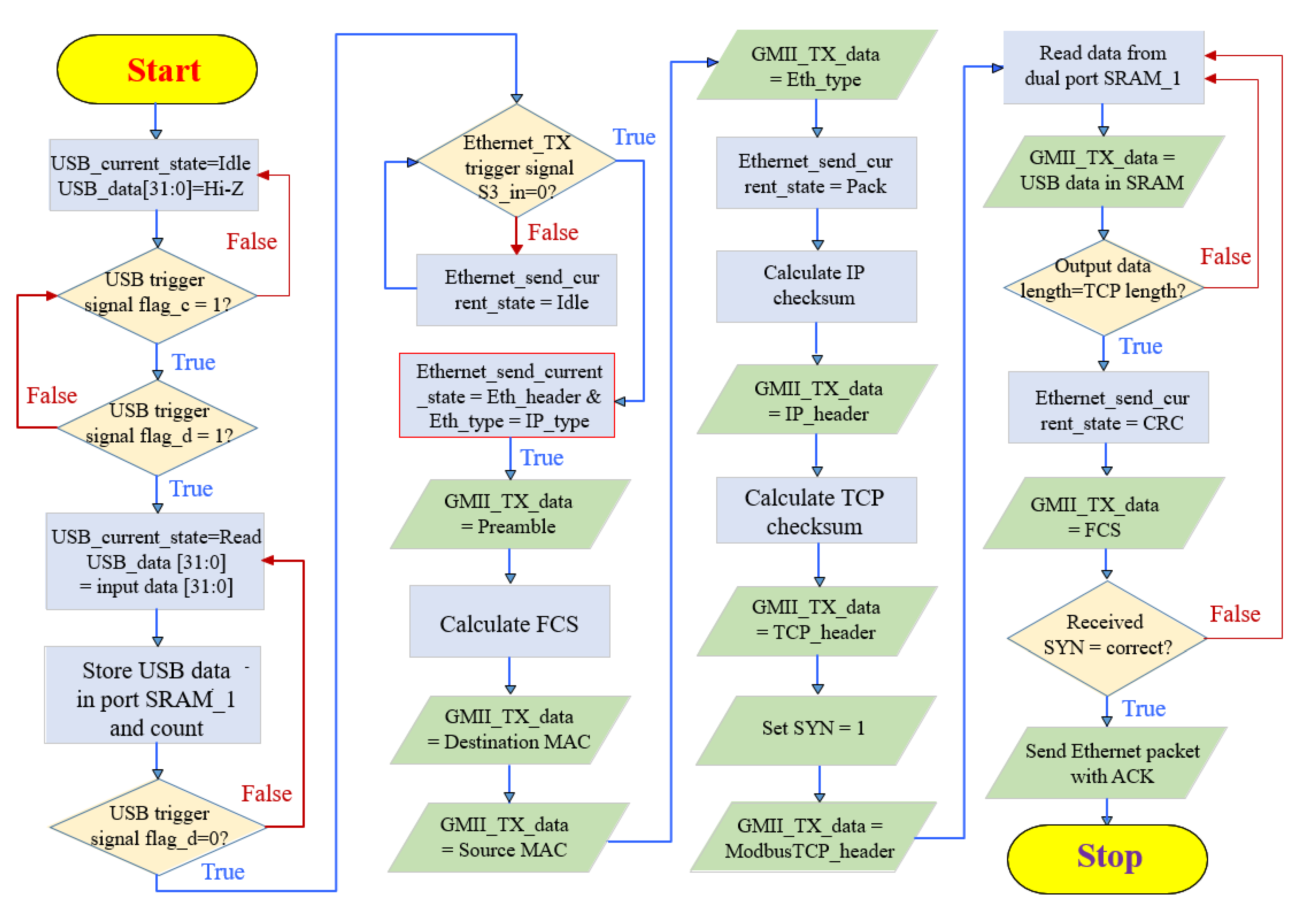
Figure 9 presents a flowchart of the process of receiving USB data from the USB module and converting it into an Ethernet packet. If the USB module receives the input request signal (Flag_c = 1 and Flag_d = 1), it saves the received USB data in Dual-Port SRAM_1 and the length of the received USB data is stored in the register. If the USB module receives an Ethernet request signal (S3_in = 0), it begins to transmit Ethernet Modbus TCP packets. First, the synchronization signal (preamble) is transmitted, the FCS is calculated, and the MAC address and Ethernet type are determined. Next, the IP checksum is calculated, and the IP header is transmitted to the GMII interface. The TCP checksum is calculated, and the TCP header is transmitted by setting SYN is high. The Modbus TCP header is then transmitted to the GMII interface [
7]. The USB data can be read from dual-port SRAM_1. If the USB data has been transmitted completely, the length of the USB data should be equal to that of the TCP data. Next, the calculated FCS is transmitted. Finally, an Ethernet packet is sent with ACK signal.
3. Simulation Results
The proposed transformation and transmission architecture has two transmission directions. One direction is transmission from Ethernet to USB. The proposed Ethernet module receives the Ethernet Modbus TCP packet and transmits it to USB 3.0. The other direction is transmission from USB to Ethernet. The USB module receives the USB data from the USB terminal and transforms it into a Modbus TCP packet. Those simulation parameters are displayed in
Figure 2 and
Figure 3, including the Ethernet module, USB module, and two SRAMs. The destination is to guarantee that the transmission function works correctly.
For transmission from Ethernet to USB, the Ethernet module confirms the control signals and received data types from the Ethernet Modbus TCP packets, as shown in
Figure 10. When gmii_rx_dv = 1, the Ethernet module starts to receive the Ethernet Modbus/TCP packet. After the preamble is verified, the Ethernet packet is received and analyzed in series. The received Ethernet packet is composed of preamble, destination MAC address, source MAC address, Ethernet type, payload, and FCS, while the ARP header includes operation code, source MAC address, source IP, destination MAC address, and destination IP. As the trigger signal arp_ack_tx is high, it means that the Ethernet packet is ready to transmit from Ethernet to USB.
If the received Ethernet Modbus/TCP packets (payload) are correct, they are stored in Dual-Port SRAM_2, as shown in
Figure 11. The first Ethernet packets are “00”, “01”, “02”, and “03”, which are transformed into a 32-bit serial data “00010203”, as shown in
Figure 11a. Note that the lengths of TCP output data are 80 in hexadecimal numeral system. The last Ethernet packets are “7c”, “7d”, “7e”, and “7f”. The CRC data are added at the end of the received Ethernet packet. As the write enable signal, wr_en, is low (0), the received function is stopped, as shown in
Figure 11b. All Ethernet packets have been transformed into serial data and stored in Dual-Port SRAM_2.
Next, if the received transmission trigger signals (Flag_c = 1 and Flag_d = 1), enable signal (en = 1) and address (addr) are selected, the received Modbus/TCP packets (00, 01, 02, 03), which are stored in SRAM (Dual_Port SRAM_2) as an 8-bit serial data (“00010203”), are read (START) and transmitted to the USB module as an USB data (“03020100”). When the trigger signals are off (Flag_c = 1 and Flag_d = 1), the transmission function is stopped.
Figure 12 presents the stored serial data in SRAM and the transmitted USB data with control signals. Note that the Ethernet packets (00, 01, 02, 03), the serial data (00010203), and the USB data (03020100) are the same. This means that the transmission function works correctly.
For transmission from USB to Ethernet, the USB module receives the USB data and stores it in dual-port SRAM_1. If the trigger signal (Flag_c = 1 and Flag_d = 1) is selected (START), the enable signal and the address are used as control signals in the received module. The received USB data is sequentially stored in SRAM (Dual-Port SRAM_1).
Figure 13 presents the received USB data in USB module and its serial data in SRAM. If the first group of received USB data is “03020100” in USB module, the stored serial data is “00010203” in SRAM, which is a reverse arrangement of the received USB data.
Next, the Ethernet module transmits the received USB data into the Ethernet Modbus/TCP packet. After the TCP header and the Modbus/TCP header are processed and sent out in sequence, the serial USB data, which is stored in SRAM, is read out. Because the length of the SRAM data is 32 bits and the length of the Ethernet packet data is 8 bits, the 32-bit USB data needs to be divided into four groups of 8 bits and transmitted into the GMII interface in sequence, as shown in
Figure 14.
4. FPGA Verification
Figure 15 presents the verification architecture of the proposed packet transformation and transmission interface. The Ethernet and USB modules are implemented on an FPGA board. Two personal computers, PC1 and PC2, and a photoelectric converter (STC-G3S20-11) are used to verify the function of the design. First, an Ethernet packet is generated with PC2 and is fed into the Ethernet module on the FPGA board by passing it through the Ethernet PHY board (RTL 8211EG) and the photoelectric converter. Second, packet transformation and transmission are completed with the FPGA board (DE-10 Standard) [
16]. Finally, the transformed USB data is transmitted into the USB 3.0 module (Cypress CYUSB301X) and received by PC1.
PC2 uses network packet analysis software (Wireshark) to monitor the received and transmitted packets.
Figure 16 presents the transmitted Modbus TCP packets from PC2 to the FPGA development kit. The ARP packet is sent to the FPGA board (Intel DE10-Standard) to verify the ARP protocol using packet generation software (Colasoft Packet Builder). Next, the FPGA board and the Ethernet PHY obtain the MAC address. After the verification of the MAC address, the Modbus TCP packets are transmitted to the FPGA board, as shown in
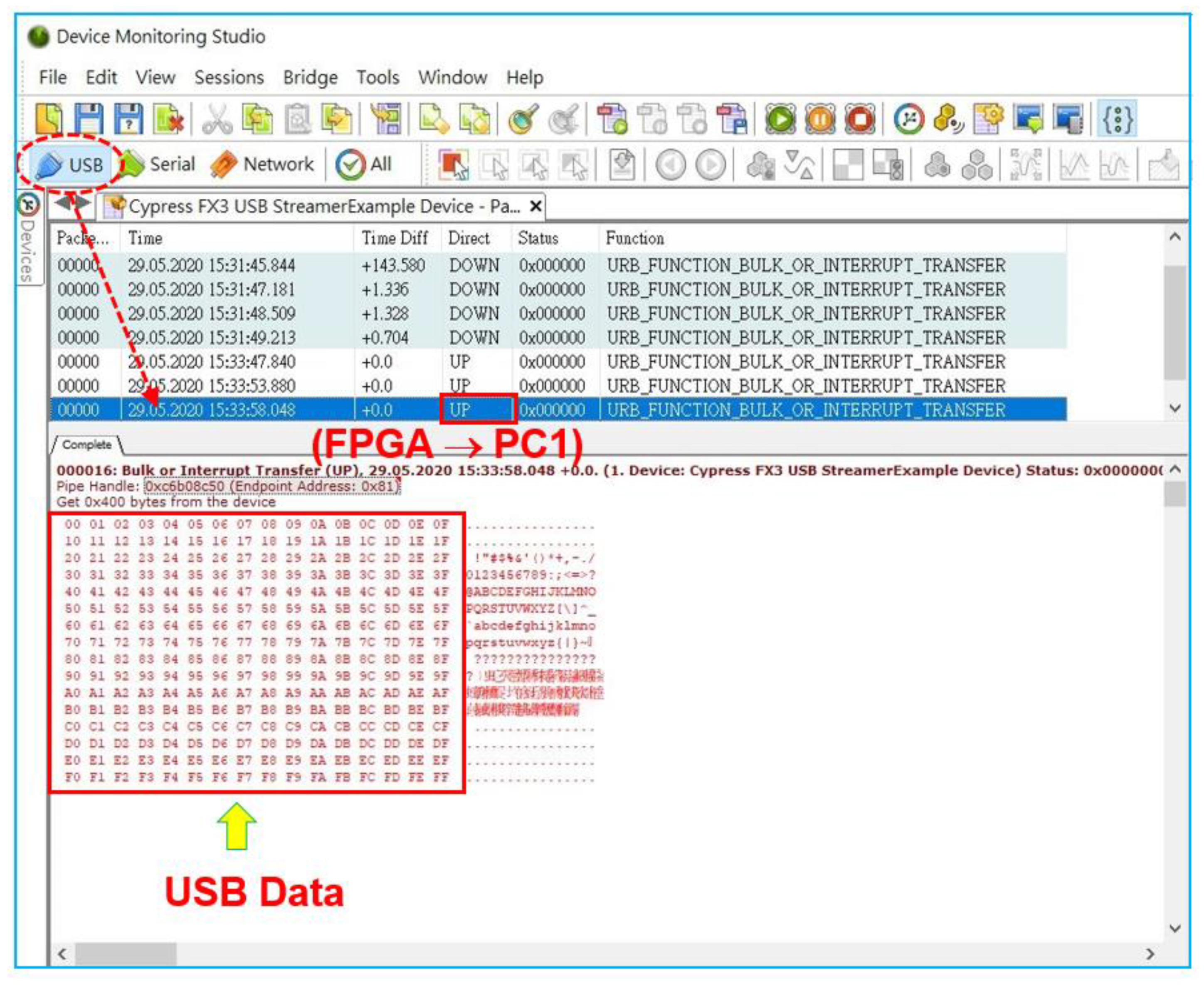
Figure 16. Finally, the FPGA board transmits the received Modbus TCP packets to PC1 via the USB 3.0 controller. The USB device monitoring software (Device Monitoring Studio) is used to monitor and analyze the transmitted USB data from USB 3.0 module, developed with a FPGA board, on PC1.
Figure 17 presents the transmitted USB data from the FPGA development kit to PC1. Those transmitted data are correct when compared to those packets in
Figure 16.
Conversely, PC1 sends USB data to the Ethernet module with Ethernet Modbus TCP packets.
Figure 18 presents the received USB data from PC1 to the FPGA development kit (Intel DE10-Standard) through the USB 3.0 controller using USB device monitoring software (Device Monitoring Studio). The FPGA board transforms the received USB data into Modbus TCP packets. The transformed Ethernet packets pass through the photoelectric converter and are sent to the CAT-5 twisted pair to connect to PC2. PC2 is used to analyze the Ethernet Modbus TCP packets.
Figure 19 shows the verification of the transformation and transmission of USB data into Ethernet Modbus TCP packets. A comparison of the transmitted packets in
Figure 16 with the received packets in
Figure 19 suggests that the proposed design is functional. By sending more packets to the proposed bridge, we cannot find the packet loss. The reliable transport of messages is completed successfully.
A logic analyzer is used to measure the latency of the transmission of the Ethernet Modbus TCP packets from the Ethernet PHY to the USB 3.0 controller.
Figure 20 presents the measured latency of the transmitted Ethernet Modbus TCP packets. When the first bit of the Modbus TCP packets is transmitted, the Ethernet PHY triggers a timer with start time of 0.000 μs. If all transmitted packets pass through the FPGA board, transformation and transmission are completed and the packets are sent to the USB 3.0 controller. When the USB receiver (USB 3.0) receives the first bit of USB data, the elapsed time is noted with finish time of 18.845 μs. The latency of the transmission of the Ethernet Modbus TCP packets is approximately 18.845 μs.
A complete Ethernet Modbus TCP packet is a 1534-byte data, which includes 8-byte Preamble, 14-byte Ethernet header, 20-byte IP header, 18-byte TCP header, 10-byte Modbus TCP header, 1460-byte payload, and 4-byte FCS. If the largest data (payload) of the Modbus TCP packet is transmitted at the processing clock frequency of 125 MHz, the processing time is approximately 12,290,641 ps for a maximum data of 1460 bytes. Then the data throughput is about 950.31 Mbps by dividing the largest data of 11,680 bits (=1460 bytes) by the processing time of 12.290641 μs.
Figure 21 shows the processing time required to transmit the largest Modbus TCP payload of 1460 bytes at the processing clock frequency of 125 MHz.
In view of the transformation and transmission between Modbus TCP packet and USB data, the processing time is reduced to 15.626303 μs because of the different processing clock frequency between Ethernet PHY and USB controller. The processing clock frequencies are 125 MHz and 100 MHz for Ethernet PHY and USB controller, respectively. If the largest data (payload) of Modbus TCP packet is transmitted between Modbus TCP packet and USB data, the processing time is approximately 15.626303 μs for a maximum data of 1460 bytes. Then the data throughput from Ethernet packet to USB data is about 747.45 Mbps by dividing the largest data of 11,680 bits (=1460 bytes) by the processing time of 15.626303 μs.
Figure 22 shows the processing time of the transformation and transmission between Modbus TCP packet and USB data at the maximum data of 1460 bytes, the processing clock frequency of Ethernet PHY of 125 MHz, and the processing clock frequency of USB controller of 100 MHz.
After the designed functions have been verified on the FPGA development kit, an application specific integrated circuit (ASIC) is fabricated in TSMC 0.18-μm CMOS process by completing the processes of synthesis, automatic placement and routing (APR), design rule check (DRC), and layout versus schematic (LVS).
Figure 23 shows the chip layout of the proposed transformation and transmission bridge between the Ethernet Modbus TCP and USB 3.0.
Figure 24 illustrates the circuit blocks of the proposed bridge ASIC using RTL Viewer software. The ASIC includes Ethernet module, USB module and two dual-port SRAMs (SRAM_1 and SRAM_2).
Table 1 provides a summary of the specifications of the proposed Ethernet and USB bridge ASIC [
14,
15].
Figure 25 shows the comparison between pre-layout simulation (UP) and post-layout simulation (DOWN) for receiving the Ethernet Modbus TCP packets, which are sent to USB controller. According to the simulated results, all Ethernet packets were received correctly in a post-layout simulation. The chip layout successfully works for the proposed bridge ASIC.
Table 2 summarizes the measured specifications of the proposed Ethernet and USB bridge developed herein with FPGA (FPGA development kit)/PL (programmable logic) and compares them with those of previous studies. The performance comparison proved that the measured throughput, latency, and power consumption in this study are superior to those reported in [
13,
16,
17,
18,
19] and that only the Modbus TCP protocol is used in this study. The TCP/IP protocol is popular in [
13,
19] and this study. Meanwhile, the ARP protocol is used in [
13,
17] and this article. Notably, the proposed Ethernet and USB bridge achieves the highest throughput (950.31 Mbps) and the lowest latency (18.845 μs) compared to those previous studies. A bridge ASIC was fabricated in TSMC 0.18-μm CMOS process with low power consumption of 142.17 mW.


