1. Introduction
Optical antennas are the new concept in physical optics and are the analogues of radio-wave and microwave antennas. The advancement in these optical antennas enables modern technologies to manipulate and control optical radiation at subwavelength scales [
1]. Regardless of the prevalent use of radio- and microwave antennas, these optical analogous antennas have not been developed so far in technological applications because of their small sizes and difficult fabrication techniques. These optical antennas are mostly based on the plasmonic effect, which is one of the rapidly growing research areas from the past two decades due to its wide range of applications in solar energy harvesting, biosensors, imaging, medicine, quantum computing, spectroscopy and optical communication [
2,
3,
4]. Many researchers have designed different plasmonic nano structures for different applications. For example, [
5] has presented nanowire waveguides for deep subwavelength confinement. The authors in [
6] prepared metallic nanowires for ultrasensitive deflection sensing. In [
7,
8,
9], the authors showed the coaxial lithography for optical and electrical properties of heterogeneous nanowires. In addition, [
8] showed the metal–semiconductor interface for lithography.
Among the applications of plasmonics, the novel optical properties such as resonant scattering and transparency are achievable from active core–shell nanoparticles for nano-sensor applications [
10]. These plasmonic-based core–shell nanoparticles also have possible applications as a localized optical sensor [
10,
11] used in biomedical sensing and imaging. Due to the tunability of plasmonic resonance in an optical regime [
12], these core–shell nano-antennas have potential use in displays. The exciting application of these plasmonic core–shell nano-antennas is their potential to be used in drug delivery [
13,
14] and cancer therapy [
15,
16,
17]. In addition to this, these core–shell nano-antennas have the ability to enhance the light-trapping behavior of solar cells and consequently can improve the conversion efficiency of solar cells [
18,
19]. These plasmonic core–shell nanomaterials also have several advantages over organic dye markers and quantum dots because they have chemical stability, low toxicity and a high signal-to-noise ratio [
20].
The spherical core–shell nano-antennas presented to date are of two types, i.e., passive and active nano-antennas [
21]. Many numerical and experimental works have been presented on passive core–shell nano-antennas, such as Ag-coated SiO
2 nano-antennas [
20,
22,
23,
24,
25], unidirectional scattering by magneto-electric core–shell nanoparticles [
26], a gold nanoparticle-based core–shell [
27] and self-assembled 3D arrays of Au-SiO
2 core–shell nanoparticles [
28]. Likewise, some active core–shell nanoparticle antennas have been presented purely based on simulations, e.g., active cylindrical and active coated nanoparticles [
29], scattering from active core–shell nanoparticles [
21,
30,
31], active coated nano-toroid antennas [
32], core–shell arrays with more stability [
33] and plasmonic-induced polarization rotation [
34]. Some of these arrays of core–shell nanoparticles work out the enhancement of the optical characteristics, such as what is presented in references [
29,
32,
33,
35]. Unfortunately, all the active core–shell arrays, as well as the passive core–shell arrays, experience the problem of instability, as the basic units reported till now are placed in open air or in an aqueous solution [
27,
28,
36,
37]. However, when a dielectric occupies the spacing between CNPs to achieve stability, the destructive coupling then limits the enhancement of optical characteristics [
33]. Similarly, the arrangement of nanoparticles to construct an array for enhancing their optical properties is another issue faced by both passive and active core–shell nano-antennas [
33,
34,
38]. However, the optical properties still need enhancement for applications in nano-sensors and nano-amplifiers.
This article proposes an inverse model of the already proposed active coated nanoparticle (CNP) [
34], having silver in the core while the gain medium is in the shell; hence, it is named an active inverse coated nanoparticle (I-CNP). This active I-CNP is then combined with an active CNP and having a dielectric in between them hence constructs a new model. The optical properties of this model are compared at first with the model comprising two active CNPs having a dielectric in between them and with the model comprising two I-CNPs having dielectrics between them. A remarkable enhancement is observed for this mixed model of an active CNP with an active I-CNP in the presence of a dielectric. The dielectric is inserted in all the proposed models for achieving stability, while the size of the dielectric is optimized for the better far-field dipole pattern of scattered radiation. After comparison of the optical properties of the three models, the proposed model is extended two-dimensionally to observe its optical properties. Fortunately, the proposed model does not affect the radiating polarization of the far field. This is because the dielectric is not in a resonant state at the desired frequency when the CNPs and I-CNPs are in a resonant state.
It is important to mention here that a single active CNP may have better optical characteristics over an I-CNP, but the compacted array comprising only active CNPs [
33] or I-CNPs (shown in this article) faces large side beams due to the coupling inside the configuration, which limits the gain enhancement of the nanoparticle array, so we called it destructive coupling. Here, this research proposes that the destructive coupling is tailorable and can be decreased by combining the active CNP with I-CNP for both smaller and larger spacing between CNPs and I-CNPs. The combined structure of the CNP and I-CNP actually tailors the electric currents that orient in such directions to obey Kirchhoff’s current law, which consequently produces electric fields in such directions to support each other, hence decreasing the destructive coupling and achieving array gain to strengthen the SCS.
2. Modeling the Materials
The optical characteristics are characterized here by scattering cross-section and absorption cross-section, which can be obtained by exciting the core–shell nanoparticles with an electromagnetic planewave [
19]. Therefore, we use CST post-processing tools utilizing CST Microwave Studio, which solves Maxwell’s equations using the frequency domain method, to calculate these values of scattering and absorption cross-sections. The basic units of the configurations in this research are the spherical active coated nanoparticle (CNP) and the inverse spherical active coated nanoparticle (I-CNP). In CNP model, the erbium-doped silicon dioxide (called an active/gain medium or active SiO
2) shell surrounds silver (Ag) in the core, whereas in I-CNP model, the silver in the shell surrounds the active SiO
2 core.
The boundary condition is open and space in all directions. The mesh size and density affect the convergence of the simulation, and here the final meshes are optimized as minimum step of mesh is 5.0.
2.1. Size-Dependent Drude Model
The silver (Ag) used here is based on the size effect Drude model at optical wavelengths between 200 nm and 1800 nm. The optical response of nano-dimensional materials is tremendously different from their bulk counterpart. The relation given below provides the dielectric response of a material in terms of Drude response and inter-band transition [
30,
35].
Here, R, ωp and Γ represent the thickness of the surrounding shell, the plasma frequency and the collision frequency, respectively.
The values of all Drude parameters and Fermi velocity, used to compute the dielectric dispersion for 10 nm thick silver shell and 58 nm dielectric core, are m*/m = 0.96, N = 5.85 × 10
28 m
−3, V
F = 1.39 × 10
6 m/sec and
ωp = 1.39269 × 10
13 s
−1, as given in reference [
29]. The separation gap of CNPs and I-CNPs in all three configurations is enough large to prevent quantum tunneling or charge transfer between CNPs; therefore, the size effect in classical Drude model is termed a semi-classical model.
2.2. Lorentz Model for Gain Medium
The gain media in core of CNP and in shell of I-CNP have rare-earth-doped SiO
2. The values for gain media used in CNPs and in I-CNPs are the same as discussed in references [
29,
35,
39]. The following relation describes Lorentz model to incorporate the canonical gain media in CST Microwave Studio.
The relative epsilon of the dielectric (silicon dioxide) is set as constant
due to its low loss characteristics, resulting in the refractive index
. The optimal value for
is set for resonance frequency
and also
to obtain
and then obtain
.
Re-arrange Equation (2) and replace
with its value to obtain:
The damping frequency
is related to the resonance frequency and valued in the range (10
−3~10
−1)
to represent low to high loss materials listed in [
29,
39].
2.3. Planewave Excitation
Scattering cross-section (SCS) and absorption cross-section (ACS) can characterize the behavior of core–shell nanoparticles excited by electromagnetic planewaves. SCS is the integrated power enclosed in the scattered field normalized by the irradiance of the incident field, whereas ACS is the measure of the net power flux through a surface surrounding the concentric shells normalized by the incident field irradiance. Therefore, ACS is a measure of how much energy is being absorbed by the concentric shell structure. The scattered and absorbed power can be expressed by the following expression via Poynting’s theorem:
where
S is the surface enclosing the particle, and
is the unit vector pointing outward to the surface. The total SCS, ACS and ECS can be defined by ratio of radiated power with incidence irradiance.
The values of , and are readily calculated with the CST post-processing tools.
2.4. Designed Single Core–Shell Parameters
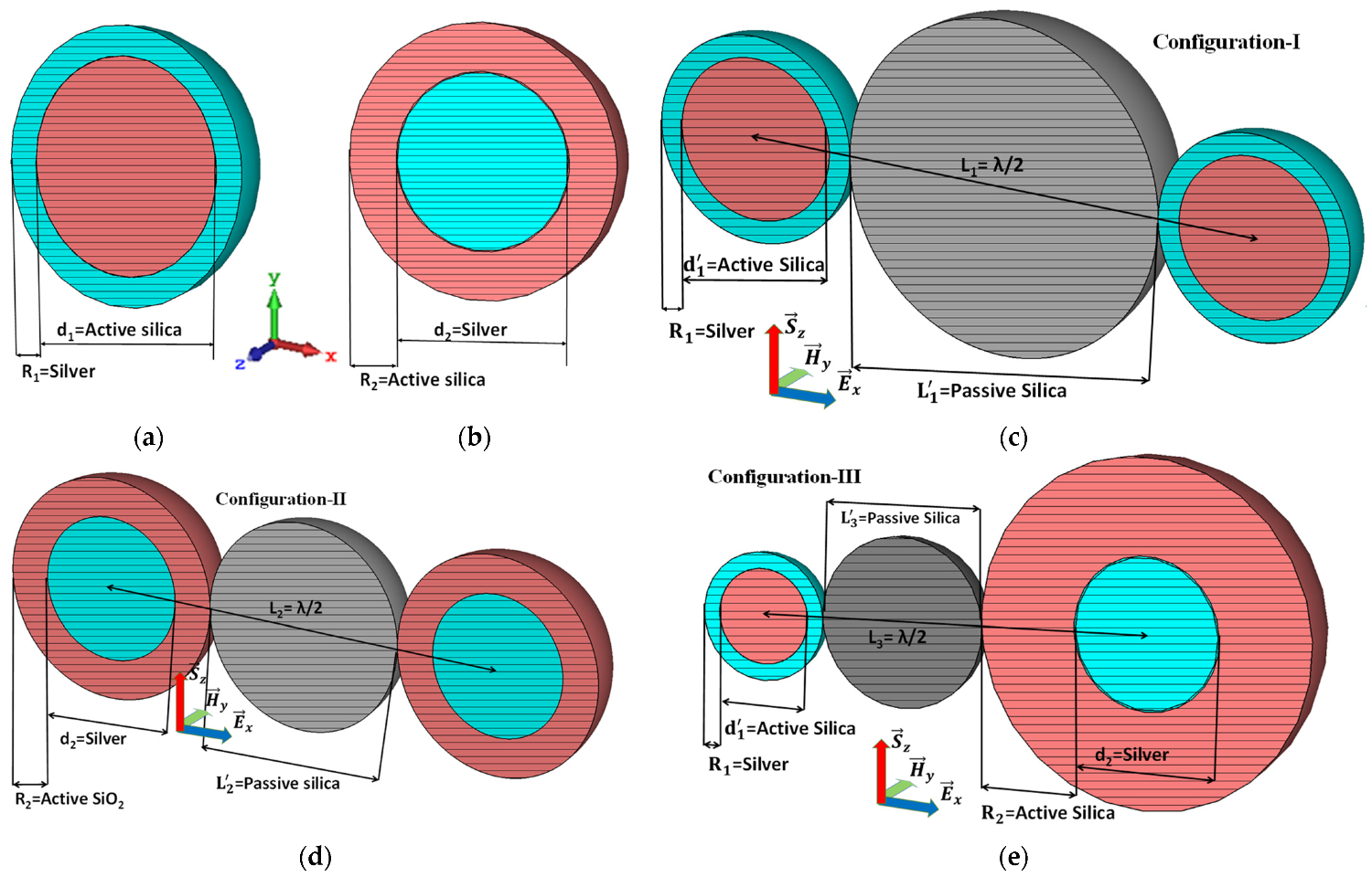
The two basic active coated nanoparticle models construct three different configurations for comparison. The first basic CNP model shown in
Figure 1a is comprised of silver in the shell of thickness “
”, and its core is filled with active silica of diameter “
”; hence, it constructs an active coated nanoparticle (CNP). Likewise, the second model in
Figure 1b consists of a silver core of diameter “
” enclosed by an active silica shell of thickness “
”. Consequently, this formulation becomes the inverse of the first CNP model, i.e., active spherical inverse coated nanoparticle (I-CNP). The resonance peaks of silver (Drude model) and active gain media were firstly optimized at a resonance frequency range of
, and then the maximum optimized thickness and diameter are selected for further simulations. These basic models further constitute three different array configurations.
2.5. Designed Parameters of the Three Configurations
In the first configuration, two active CNPs are alienated by a distance of λ/2 from their centers, as shown in
Figure 1c. The parameters of CNPs are optimized with reference to the resonance frequency. As a result, the optimized thickness of the Ag layer in a shell is the same as for a single CNP, i.e.,
, and the diameter of active silica in the core is
. The passive silica of diameter
fills here the separation between both CNPs. In the second configuration, another passive silica of diameter
combines two I-CNPs by separation of λ/2 from their centers. The parameters of I-CNPs in
Figure 1b and in
Figure 1d are the same, i.e., thickness of active silica shell is
, and the diameter of the silver core is
. Finally, in the third configuration, as shown in
Figure 1e, the passive silica of diameter
combines the CNP and I-CNP with separation λ/2. Here, the parameters of CNP and I-CNP are the same, as demonstrated in configurations I and II in
Figure 1c,d.
2.6. Optimization of Single Core–Shell Parameters
Both the radius and core material are optimizable regarding the performance of the CNP throughout the visible regime. For a constant thickness of silver in the shell, the variance in core diameter changes the resonance frequency peak of the CNP. For example, increase in core diameter shifts the resonance peak of CNP towards lower frequency and vice versa. The optimization of I-CNP follows the same process, where the variations in shell thickness keep the resonance peak variant. Here, the selected thickness of silver (Drude model) and diameter of active SiO
2 were first optimized in CST through simulations. For this purpose, different diameters of active SiO
2 were optimized at desired resonance frequency f
o = 600 THz, while the thickness of shell was kept constant (silver peak is adjusted at resonance frequency f
o = 600 THz), as shown in
Figure 2a. Similarly, in the case of I-CNP, the diameter of the silver core is constant, whereas the thickness of gain media in shell is optimized to the desired resonance frequency, as shown in
Figure 3a.
3. Single Active CNP and I-CNP Results for Planewave Excitation
The
polarized planewaves propagating in the
direction excite the individual CNP and I-CNP models at first to obtain their optimized scattering cross-section, absorption cross-section, electric field pattern, power flow and far-field pattern at resonance frequency. The amplitude of this incident planewave is
V/m and can be express as:
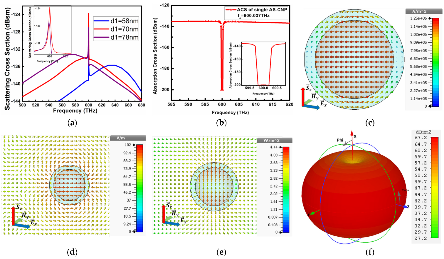
Figure 2 shows the labeled diagram of CNP whose similar design is discussed in references [
33,
34] but for a different thickness of shell and its respective core diameter. Here, a different shell thickness of the CNP is simulated according to the requirements that are explained in detail in
Figure 2.
Table 1 shows the optical properties of an individual CNP at
resonance frequency when excited by
polarized planewave, whereas
Figure 2 gives the diagrammatical illustration of the optical properties shown in
Table 1. Here, the scattering cross-section peak, shown in
Figure 2a, is −124.66 dBsm, which is 10 dB higher than the ground value, whereas the minimum absorption cross-section reported in
Figure 2b is −200 dBsm, which is 65 dB lower than the ground value.
The current density in
Figure 2c is
, whereas the electric field in
Figure 2d is
. Similarly, the arrows in
Figure 2e denote
power generating from the center of the CNP flowing towards and away from the source planewave direction. In addition to this, the far-field pattern in
Figure 2f supports the power flow along the z-axis, providing a dipole pattern of
gain.
The selection of frequency interval and numerical analysis are the same as for the CNP, as the expected resonance frequency is
.
Figure 3a,b depicts the scattering cross-section and absorption cross-section of I-CNP when excited by planewaves. The peak SCS reported in
Figure 3a is −117 dBsm, which is 13 dB higher than the ground value and again is very close to the anticipated resonance frequency
. On the other hand, the ACS reported by
Figure 3b is −200 dBsm, which is 50 dB below the background value.
Figure 3c–f elaborates the predicted numerical results of the current density, electric field, power flow and far-field pattern, respectively. The highest current density at the resonant state presented in
Figure 3c is
, while the stated electric field is
in
Figure 3d. The resonant dipole field in the I-CNP pushes power out of its y-axis, i.e., from the center, and pulls it towards the source side, forming vortices around its poles. In addition to this, the radiated power from the center of the I-CNP is
, as publicized in
Figure 3e at a resonance frequency of
. Similarly, the strong dipole realizes
gain at the resonance frequency shown by the far-field pattern in
Figure 3f.
4. Results Comparison for Array Configurations
The
polarized planewave excites the three configurations, sketched in
Figure 1c–e, to compare their optical characteristics near the desired resonance frequency.
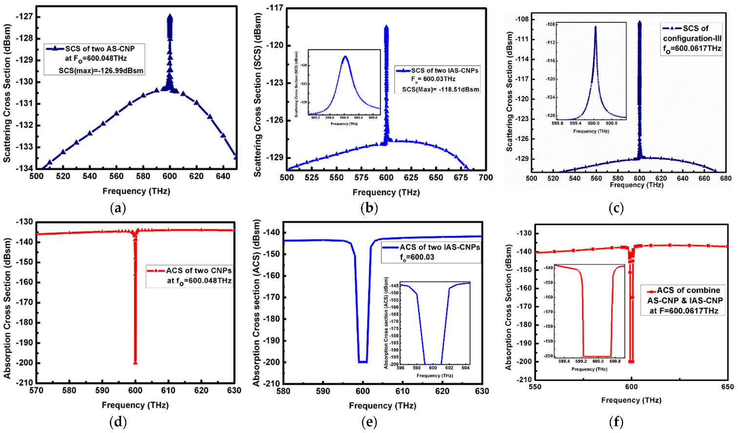
When a passive dielectric of λ/2 size combines the two CNPs (configuration I), the resonance frequency of the CNPs then displaces from the desired frequency. Therefore, to bring the resonance states of both CNPs at the desired frequency, we optimize the size of the gain media in the core of the CNPs. The SCS peaks in
Figure 4a show the optimization of gain for configuration I, where the optimized size of the core is 58 nm.
In case of configuration II, the inclusion of a passive dielectric does not affect the resonance peak of I-CNPs from the desired frequency. Therefore, configuration II does not need an optimization of parameters.
Similarly, in the case of configuration III, the parameters of CNP and I-CNP are the same as for configuration I and II, respectively.
4.1. SCS and ACS Comparison of the Three Configurations
Figure 4a reports
for configuration I at a frequency
, which is
higher than the ground value. It is a decrease of
from the SCS of the single CNP, reported in
Figure 2a. Likewise,
Figure 4b shows maximum
at
for configuration II. It is
higher than the ground value. In comparison with the single I-CNP model, it is almost similar to the SCS of the single I-CNP reported in
Figure 3a. Despite this, the maximum SCS reported in
Figure 4c is
for the third configuration, at
, which is
higher than the ground value.
It is noticeable that due to destructive coupling, the maximum SCS peaks reduce for the first two configurations as compared to the single CNP and I-CNP models, but for the desired configuration III, the SCS boosts. Moreover, the SCS for configuration III is greater than the SCS of configuration I and greater than configuration II. Adding to this, the minimum of ACSs for configurations I, II and III are and below the background values reported in d, e and f, respectively.
4.2. Analysis of E-Field and Current Densities
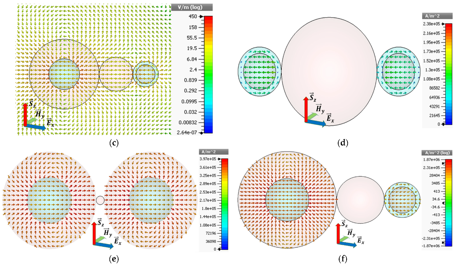
Figure 5a–c illustrates the electric field of the three array configurations. The maximum values of the electric field for configurations I, II and III are
,
and
, respectively, at their respective resonance frequencies. A clear coupling of the near E-field is observable in
Figure 5a,b. On the other hand, the electric field for configuration III enhances to
as shown in c. This configuration provides a large enhancement of electric fields because the selection of materials in the core and shell is articulated in such a way that the near-electric field of both individual formulations strengthens the electric field instead of the opposition.
Figure 5d–f represents the current densities of the three configurations. The maximum values for the current densities are
and
for configurations I, II and III, respectively. By comparing the current densities of configurations I and II with their single CNP and I-CNP models, as shown in
Figure 2c and
Figure 3c, the decline due to coupling is clear. Similarly, for configuration III, the current is stronger than configurations I and II, as well as from the individual CNP and I-CNP. From
Figure 5f, the direction of the current in the I-CNP is directed from the silver in the core to the gain medium in the shell. In the CNP, it is directed from a gain medium in the core towards the silver in the shell, which strengthens the peak of the current density and corresponds to the electric field distribution in
Figure 5c.
4.3. Analysis of Power Flow and Far-Field Pattern
Figure 6 reports the power flow and strong dipolar far-field pattern of the three configurations.
Figure 6a–c reports the power flow for the three configurations as
and
, respectively. In all configurations, power is pointing out from the gain media and flows towards the source. The power flow for the first two configurations decreases as compared to their single basic models due to coupling. The power flow for configuration III enhances almost five times as compared to the power flow of both configurations.
The far-field pattern in
Figure 6d shows a
scattering cross-section (SCS) for configuration I, which decreases by
from its single CNP model (as discussed in
Figure 2f). Similarly, for the second configuration, the SCS is
, as shown in
Figure 6e, which is a decrease of
gain from the single I-CNP model (described by
Figure 3f).
Figure 6f reports a
SCS for configuration III. It is
and
higher than configuration I and II, respectively. It is also higher than the individual CNP and I-CNP.
For the far fields in
Figure 6, the beam widths in the
xoz plane are thinner in
Figure 6d,e but fatter in f, which means that the directivities are larger for configurations I and II than that of configuration III. However, the peak values of the SCS in
Figure 6d,e are smaller than that in
Figure 6f. It is clear that the radiation efficiencies of configurations I and II are smaller than that of configuration III, which depends on the combination structure of configuration III.
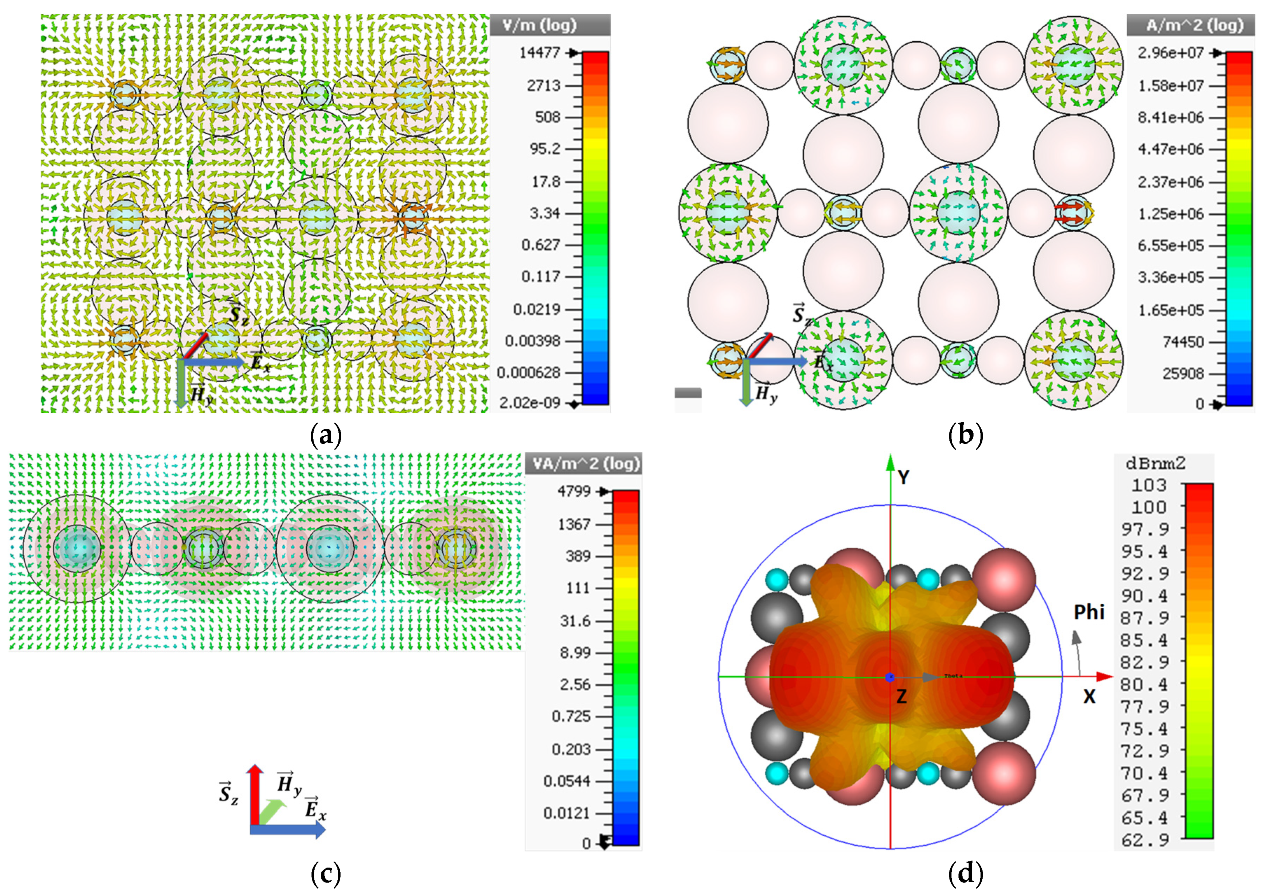
6. Extension to Array Model
Here, we propose the arrangement of CNPs and I-CNPs for the formation of an array model in the presence of a passive dielectric medium, where the passive dielectric provides the stability to resonators as well as behaves as a capacitor to prevent losses of energy. The extension of the array model constitutes from repetitions of configuration III.
Figure 7a shows the array model where the 10 nm silver shell enclosing the gain media in a core of diameter 58 nm constructs the active CNPs, whereas the 94 nm shell of gain media enclosing the silver in a core of a diameter of 60 nm forms the I-CNPs. The passive silica of diameter
combines these CNPs and I-CNPs in rows. The passive dielectric also fills the separations of CNPs and I-CNPs in a column along the y-axis, which is
. The
polarized planewave propagating along the z-axis excites the array model.
The maximum SCS obtained when the extended array radiates is
, which is nearly
higher than the background values and
higher than SCS reported for configuration III. Furthermore, the minimum of the ACS is
below the background values reported in
Figure 7c.
The electric field and current density are shown in
Figure 8a,b with peak values of
and
, respectively, which increase more than 10 times of the single configuration III. Likewise, the power flow in
Figure 8c enhances to
, which is also an increase of more than 10 times as compared to single configuration III. In addition to this, the arrows denoting power flow in c are generating from gain media and project towards the source planewave direction. This direction of power flow is verified by the directive beam of the far-field pattern in
Figure 8d, which points a maximum of
gain along the z-axis, i.e., towards the source direction. The radiated electric field of the entire three rows of the model reports fewer coupling effects and gives highly directive-scattered radiation in the planewave direction instead of scattering in all directions.
8. Conclusions
An inverse active spherical coated nanoparticle (I-CNP) is designed and combined with a CNP for array formation to enhance the optical characteristics. Consequently, three different configurations of active core–shell nano-antennas were compared for optical characteristics. The electric field, radiated power, scattering cross-section and far-field gain for configurations I and II were reported as 114 V/m and 25 V/m, 0.89 VA/m2 and 0.243 VA/m2, −126 dBsm and −118 dBsm and 56.7 dBnm2 and 65.5 dBnm2, respectively, whereas the enhancements in these optical parameters for the proposed array constitutes from configuration III are reported as 450 V/m, , −108 dBsm and 73.8 dBnm2, respectively. The results revealed that the configuration (III) having active spherical CNPs with their inverse active spherical CNPs shows the most suitable results, in comparison to that of the configurations that have two active spherical CNPs (I) or two inverse active spherical CNPs (II), due to tailoring with the core–shell material to reduce destructive coupling in the presence of small passive elements. Analysis demonstrates that the configuration of a CNP with its I-CNP separated by a passive dielectric can improve the optical characteristics and is worthy for nano-amplifier and nano-sensor applications.
