Article

Design of a Power Splitter Based on a 3D MMI Coupler at the Fibre-Tip

1
Faculty of Electrical Engineering and Information Technology, Institute of Electronics and Photonics, Slovak University of Technology in Bratislava, Ilkovicova 3, 81219 Bratislava, Slovakia
2
Department of Physics, Faculty of Electrical Engineering and Information Technology, University of Zilina, Univerzitna 1, 01026 Zilina, Slovakia
*
Authors to whom correspondence should be addressed.
Electronics 2022, 11(18), 2815; https://doi.org/10.3390/electronics11182815
Submission received: 9 August 2022 / Revised: 30 August 2022 / Accepted: 2 September 2022 / Published: 6 September 2022
(This article belongs to the Special Issue Advances in Optical Channel Waveguides)

Abstract

:
Planar MMI couplers based on inorganic material platforms have played an essential role in photonic integrated circuits development. Advances in organic polymer fabrication techniques enable the design of components beyond a single plane, thus facilitating vertical integration for a wide range of components, including the MMI coupler. This paper presents the design of two 3D IP-dip polymer-based MMI power splitters operating in the near-infrared part of the spectrum at a wavelength of 1550 nm. The resulting output power ratio, modal field distributions, spectral characteristics, and the effects of input fibre misalignment are investigated using the beam propagation method. The fabrication method used to realise the designed splitters was direct laser writing. The function of the splitters was then verified by a highly resolved near-field scanning optical microscope.

1. Introduction

The multi-mode interference (MMI) coupler offers an alternative solution to the common directional coupler while maintaining output power balance, low loss, and high fabrication tolerance. The MMI coupler solidified its place in photonic integrated circuits (PIC) due to its versatility and favourable characteristics. The applications of the MMI coupler cover a wide range, starting with basic power splitting [1,2,3], switching [4,5], polarisation dividing [6], multiplexing [7,8], sensing [9], and, more recently, it has even been used in PICs for machine learning [10].
Most of the aforementioned MMI devices were based on conventional semiconductor material platforms, such as a silicon-on-insulator (SOI), III-V semiconductor materials, and lithium niobate (LiNbO3). Each one of these platforms comes with its advantages and disadvantages, be it the low manufacturing cost and small footprint (SOI) [11,12], wider band gaps, monolithic integration of light sources and detectors (III-V semiconductors) [13,14,15], or the electro-optic effect for modulating (LiNbO3) [16]. All these material platforms are mostly bound to planar structures fabricated using conventional photolithography and etching processes. The design of the MMI coupler was thus bound by the available fabrication methods, and as a result, the design process has not been significantly changed since the review published by Soldano and Pennings in 1995 [17]. The most recent progress in this area amounts to algorithmically optimized topologies and specialised software tools meant for the fast prototyping of MMI-based devices [18].
The counterpart to the conventional inorganic platform is devices based on organic materials. In the scope of passive photonic devices, the advantages of organics are their temperature-independent operation, easy integration with other components, and low-cost 3D structure fabrication [19]. Commonly used fabrication techniques are direct laser writing (DLW), self-organization, and soft lithography. In contrast with the top-down lithography methods used for inorganic platforms, these techniques are not universally applicable, since the mechanisms which form the desired patterns depend on the material itself. Self-organisation utilises the self-assembling properties of colloidal suspensions. The suspension colloidal polymer particles (PMMA, polystyrene, etc.) form crystal layers upon the removal of the solvent. The resulting one- (1D), two- (2D), and three-dimensional (3D) photonic crystals show optical properties suitable for use in photonic devices [20]. Soft lithography is a collection of techniques for patterning substrates with an elastomeric stamp (generally made of polydimethylsiloxane (PDMS) from the micro- to nanoscale) [21]. Finally, the DLW technology utilises a laser beam to scan over a layer (or volume) of organic material to form the desired pattern. Two mechanisms are used during the DLW process: photoablation and photopolymerization. The photophysical photoablation produces the pattern by melting and/or vaporising the substrate matter, commonly PDMS, polyimide (PI), and polyethylene terephthalate (PET). For 3D structures, photopolymerization is used, specifically the two-photon absorption (TPA) [22]. During the TPA process the femtosecond laser beam is focused into the material by a high numerical aperture (NA) objective lens. The shape of the structure is then realised by scanning through the volume of a suitable photoresist. Prepolymer resists commonly used for this technique include SU-8 and IP-Dip.
The capabilities of DLW process make ground for low-cost and rapid prototyping of 3D passive photonic structures. Power splitters based on this fabrication approach could provide a solution for extending PIC design beyond a single plane and raise the degree of photonics integration as such. One of the early proposals of this kind of design approach dates back to 1999, when Garner et al. described vertically integrated waveguide polarisation splitters utilizing polymers realised by shadow mask reactive ion etching (RIE) [23]. More recent research by Weigel et al. presents vertical interconnects based on a resin 3D 1 × 1 MMI coupler and proposes a multilayer waveguide routing concept [24,25]. Another form of optical interconnect was realised in the form of 3D-printed multimode-splitters fabricated using a commercial Nanoscribe DLW system [26]. These splitters were designed for the input mode size of 1.2 μm, and the input optical signal from the laser diode source was coupled into the waveguide facets utilising a 50× microscope objective with NA = 0.8. The operating wavelength (λ0) of this system was 632 nm and splitters lengths in the propagation direction were equal to 52 μm. The DLW process also offers solutions for coupling the input from the optical fibre into the waveguides of photonic devices (either planar or 3D) and vice versa. A few different couplers were proposed so far. These include a waveguide-to-fibre coupler which is used to rotate the direction of the incoming light into the planar direction and to convert the mode field diameter of an optical fibre to the size of a nanophotonic waveguide, thus eliminating the need for periodic grating which would otherwise be needed to compensate for the abrupt change in propagation direction [27]. Another example is a 3D-printed fibre socket that integrates a focusing lens. This approach by design ensures proper fibre alignment with the component, thus making it convenient for testing and prototyping [28]. Both examples were fabricated using the Nanoscribe DLW system.
This paper presents a design of 3D MMI polymer-based power splitters for direct attachment to fibre-tip using a supporting structure based on the previous work of Mizera et al. [29]. The splitters were designed for an operating wavelength of 1550 nm. The output optical characteristics of the splitters were simulated and verified by measurements. In addition, the effects of the input fibre alignment on the output field, as well as the spectral characteristics of the designed splitters, were simulated. The proposed structures bring a novel approach to the coupling of the input signal and demonstrate the flexibility and advantages of different 3D geometries based on polymer materials.

2. Materials and Methods

The self-imaging principle, on which the MMI coupler is based, was described as soon as the 19th century. The first MMI couplers designed for use in integrated photonics were extensively researched since the 1990s [17]. The base structure of an MMI coupler is a multi-mode waveguide that supports a large number of propagating modes, usually with a single-mode waveguide at the input and an appropriate number of single-mode output waveguides at the end. The beam propagation method (BPM) is a suitable tool for the simulation of such devices because of the absence of abrupt changes in the direction of propagating light. In the case of conventional planar structures, the 2D BPM simulation model is capable of providing accurate results excluding the effects of the fibre alignment.
Conventional MMI couplers used for splitting are composed of the input waveguide, the MMI section, and the output waveguides for outcoupling the split signal. The dimensions of the MMI are determined by several factors. The fixed ones include the refractive indices of the core (nf) and the cladding (nc) materials, and the operational wavelength of the device (λ0) in the material platform uses the values of nf = 1.53 (Nanoscribe IP-Dip) [30] and nc = 1 (air). The other fixed factor is the character of the input mode. In this case, it is the mode supported by a single-mode fibre (SMF) onto which the prepared MMI coupler is attached. The SMF modal field is radially symmetrical with a gaussian distribution of power and a diameter of ~9 µm. The width of the MMI (W) should then allow for the output modes, which closely resemble the input, to be separated without introducing additional interference. This means that in the case of two output modes, the width should be ~18 µm (two times the input mode field diameter); with three it should be ~27 µm. The characteristic beat length of the coupler (Lπ) can be obtained from Equation 1, where W stands for the width of the MMI coupler [17].
L π 4 n f W 2 3 λ 0
However, an additional limitation stems from the fabrication technique used. The DLW system is capable of realising structures up to 300 µm in length. Since the operational wavelength and refractive index of the core are fixed, this leaves only the width to be adjusted to satisfy the length requirement. The length limitation could be overcome by fabricating the structure in multiple steps and bonding the parts afterwards. However, the MMI, and the interfaces between the waveguides and the MMI, must be prepared in a single step, because the additional bonding interface introduces distortion of the mode field. This distortion is unpredictable regarding the function of the complete splitter [31]. This design approach should be applicable for any symmetrical 1 × N MMI splitter realised by DLW, provided the SMF input modal field is used.
Two designs were used for evaluating MMI splitters by simulation. One with a direct fibre attachment, and one using a tapered input waveguide (Figure 1). The fabricated designs used the tapered input waveguide for both 1 × 4 and 1 × 9 splitters. The dimensions of the tapered input waveguide were 10 µm in width on the fibre side and 9 µm in width on the MMI side, with a length of 60 µm in both fabricated structures.
Considering the design requirements, two MMI splitters were designed and fabricated. One with four interference maxima at the output (1 × 4 splitter) and one with nine interference maxima (1 × 9 splitter). Different simulation models were created for each of the MMI splitters, with power monitors throughout the structures (Figure 2). The power monitors divided the simulated structure into four and nine monitored domains, respectively.
The simulated characteristics of the splitters included the total power transmitted, the power distribution in different propagation lengths in the MMI splitter, the shape of the modal field at the end of the structure, and the spectral characteristics. Based on the results of the simulations, the width and the optimal length of the MMI were determined. The effect of the input offset was also studied and evaluated using the optimised simulation models.

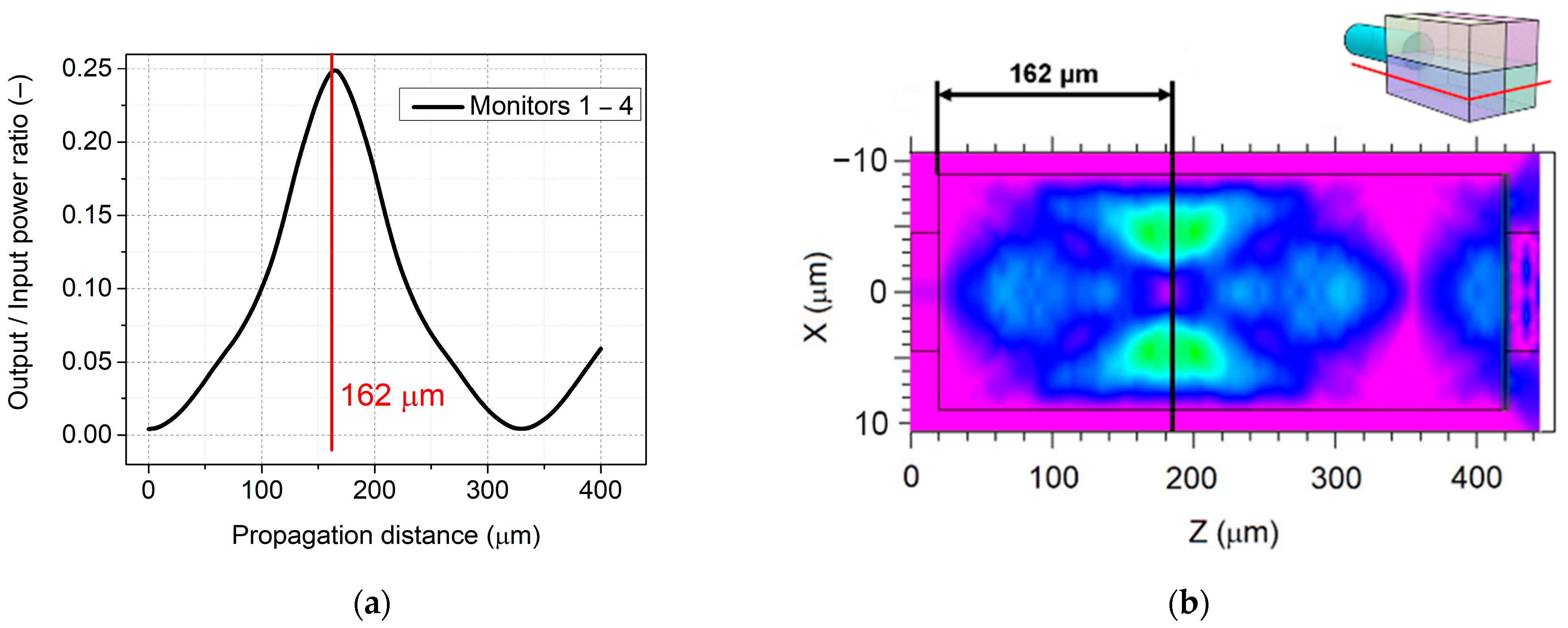
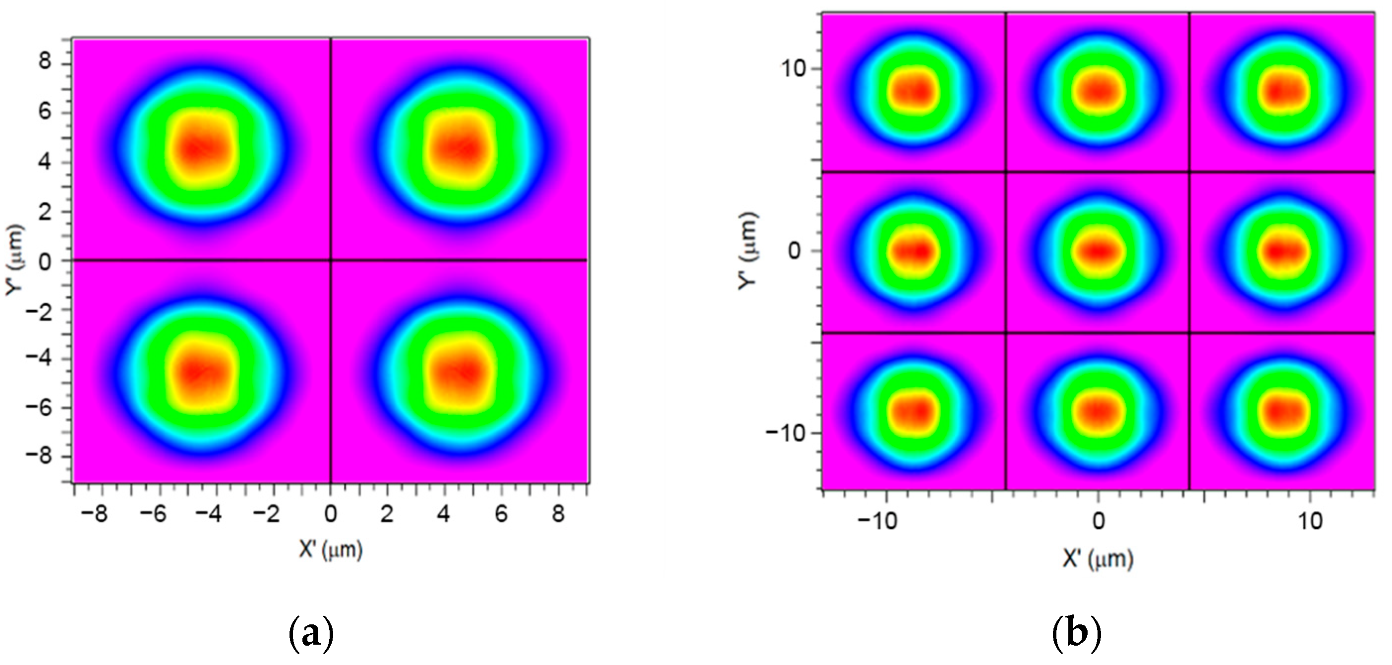
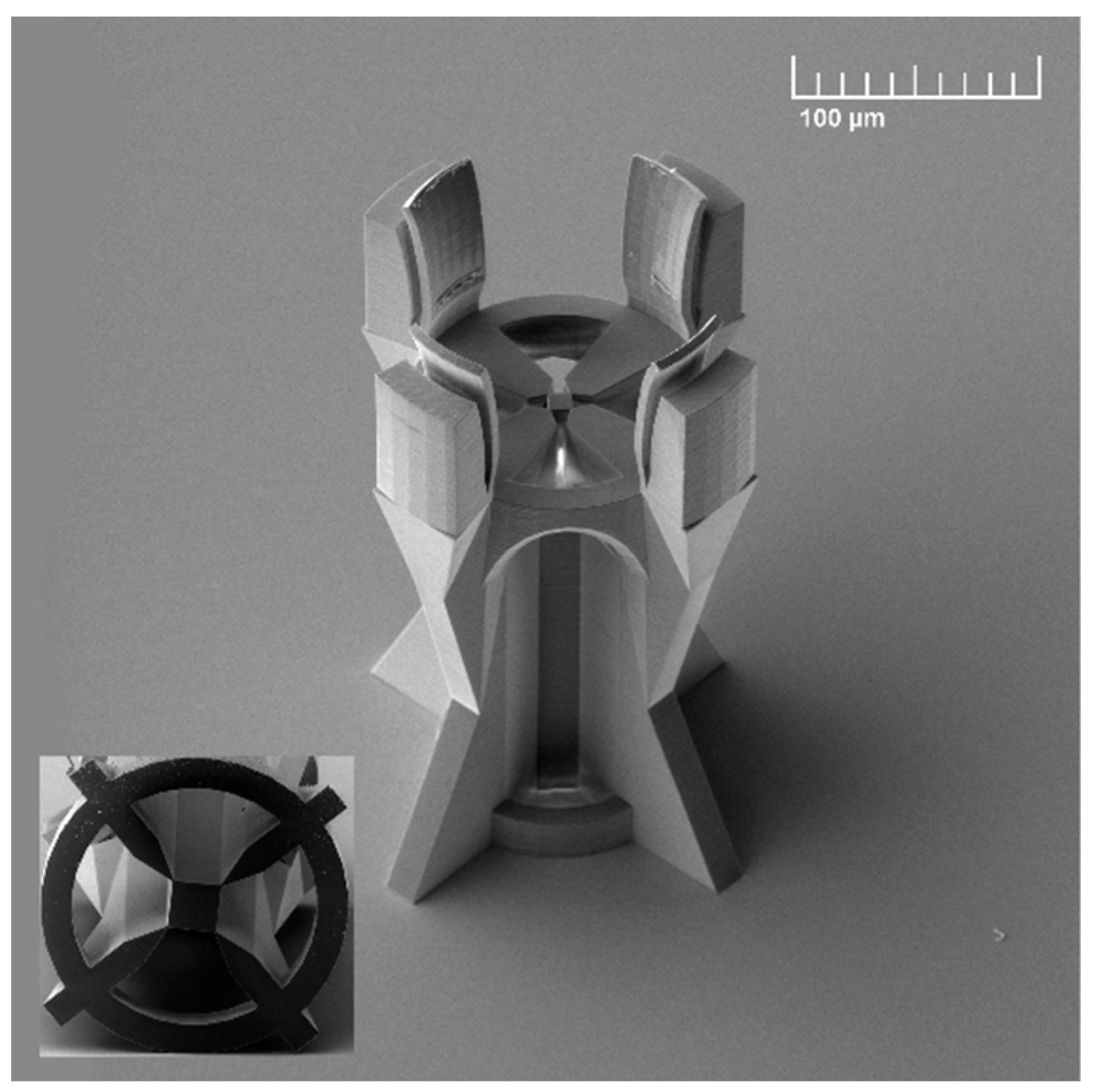
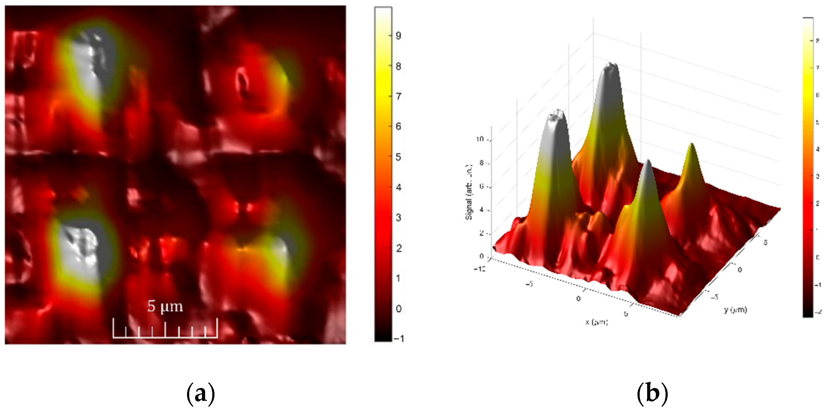
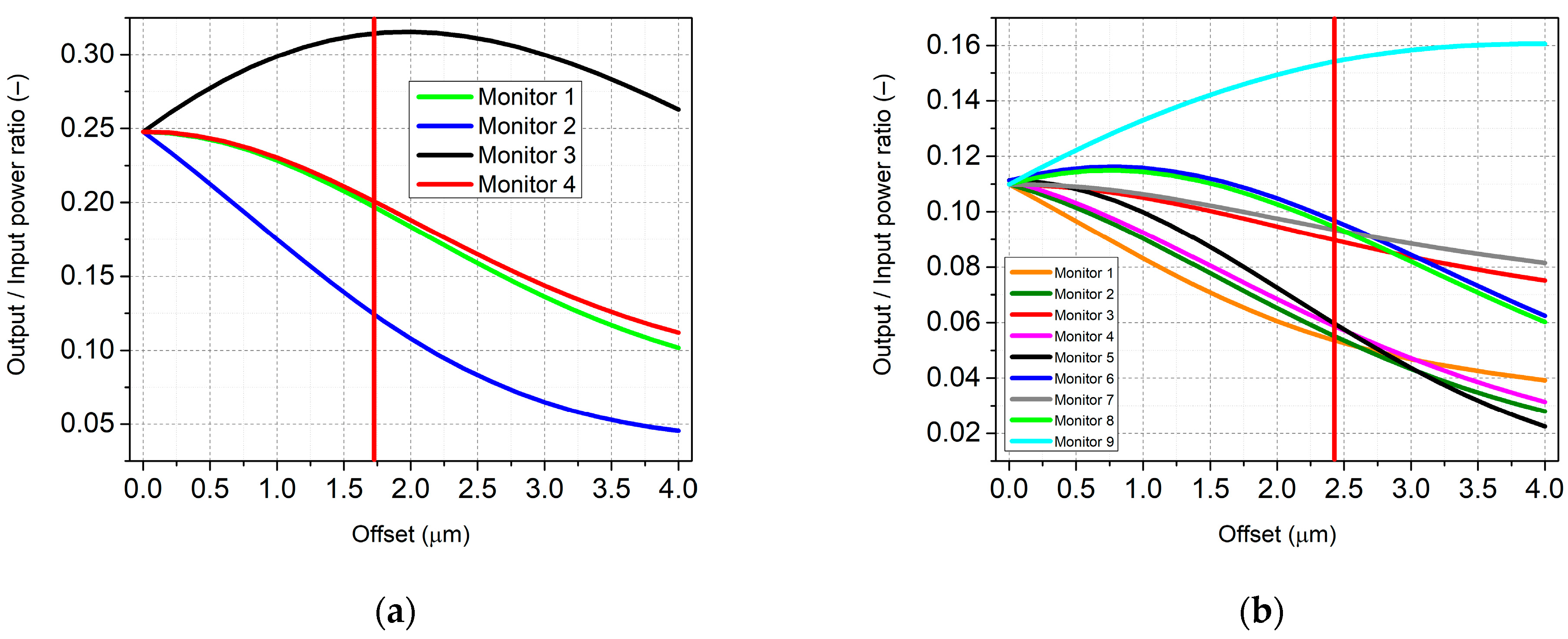
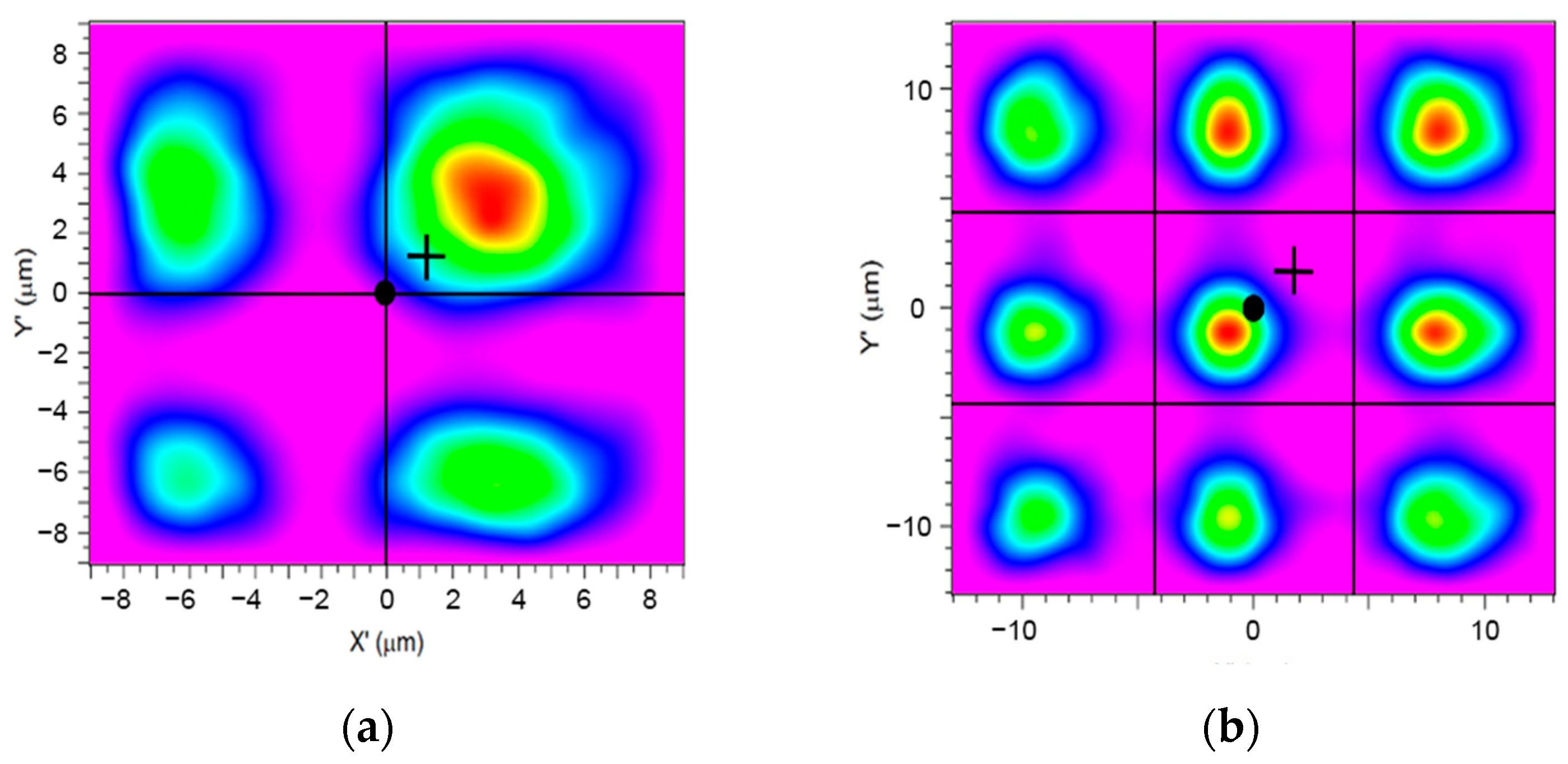
3. Results and Discussion

First, the width of the MMI (W) was determined with consideration of the design limitations. The width equal to two times the input diameter (W = 18 μm) was used for the 1 × 4 splitter. In the case of the 1 × 9 splitter, the width was reduced from three times the modal field diameter (27 μm) to 26 μm. This way the optimal beat length was reduced to fit the fabrication requirements without an impact on output interference fields.
The optimal beat length values were then simulated to be Lπ = 162 μm in the case of the 1 × 4 splitter and Lπ = 225 μm in the case of the 1 × 9 splitter. The power distribution in the MMI splitters throughout the propagation length along each output axis with modal field distribution cross-sections can be seen in Figure 3 and Figure 4. In the case of the 1 × 4 splitter the outputs were symmetrical throughout the structure, so the curves overlapped. In the 1 × 9 the interference distributed the power from the central monitor into the remaining ones.
To further verify the functions of the MMI splitters, the output modal field distributions (Figure 5) were analysed at the end of the MMI. Both splitters show distinct maxima without significant distortion. The interference images retain the shape of the input modal field and the insertion losses for all outputs do not exceed −0.75 dB in total for both designed couplers. It must be noted that the simulation doesn’t consider the surface imperfections of the device interfaces which cause loss by light scattering. However, for the purposes of the optimisation of the splitters, omitting these losses should have a negligible impact.
For a more complex analysis, the spectral characteristics of the splitters (Figure 6) were simulated. These characteristics show that both splitters fulfil their intended function beyond the wavelength of λ = 1550 nm they were designed for. The output power distribution in the 1 × 4 splitter is perfectly symmetrical throughout the spectrum, whereas in the 1 × 9 splitter it is symmetrical only from ~1300 nm and above (for wavelengths used in optical communication systems). The insertion loss in single output decreases under half power (−3 dB) at ~900 nm in the case of the 1 × 4 splitter and ~1250 nm in the 1 × 9 splitter. However, the modal fields become distorted higher in the spectrum, effectively reducing the usable bandwidth of the splitters. The modal fields retain the correct distribution down to ~1120 nm in the case of the 1 × 4 splitter and ~1400 nm in the case of the 1 × 9 splitter.
Both splitters were fabricated and characterized to validate the simulation results. For the fabrication of the 1 × 4 MMI splitter, the IP-Dip photoresist was used in a single-step process based on DLW using TPA. The commercial Nanoscribe Photonic Professional GT laser lithography system based on DLW was the crucial technology for the fabrication of the MMI splitter. The IP-Dip photoresist was used in immersion laser lithography (DILL) mode, where the lens was immersed in a liquid photoresist. In the exposed volume, the IP-Dip photoresist polymerized due to the TPA. After the polymerization process, the sample was developed in propylene glycol monomethyl ether acetate (PGMEA). The 1 × 4 splitter was prepared with a tapered input waveguide with a square profile. A tapered input waveguide with a circular profile was used for the 1 × 9 splitter. Figure 7 shows an SEM image of the prepared 1 × 4 MMI splitter.
Characterisation of the modal distribution across the output part was carried out using a highly resolved near-field scanning optical microscope (NSOM). A NSOM uses a very sharp optical fibre probe with a lateral resolution better than 100 nm, collecting the optical field at the output splitter’s surface in very close proximity [32]. Light from a fibre-coupled laser source with a central wavelength of 1550 nm was directly connected to the input waveguide. The near-field distribution near the output was measured in transmission mode.
The measured distributions in Figure 8 and Figure 9 closely resemble the distributions acquired by the simulations. Further details about the fabrication and NSOM measurements of the 1 × 4 MMI splitter are available in our previous work [33].
The size of 1 × 9 MMI was outside the range of the maximum area measurable by NSOM, so one of the maxima is not present in the measured intensity distribution. Although one can see that the 1 × 9 MMI splitter fulfils its function even with the cropped image, the number of peaks and their separation is clearly visible. The observed maxima are separated by ~8.3 μm and correspond with the simulation in Figure 5. Furthermore, the shape and intensity distribution reflect the simulated results.
Both splitters show a bias towards one of the corners of the structure. This phenomenon could be explained by the off-centre position of the input fibre in relation to the input waveguide, or by the shift of the input modal field in the input fibre itself due to the bending of the fibre in the measurement setup. The effects of the input fibre position shift were verified by the simulations in the following section.
The position of the input waveguide in conventional MMI splitters is fixed in the centre of the multimode waveguide. The attachment of the designed 3D splitters to the end of the optical fibre poses new challenges in terms of the alignment of the input and the fibre. For the simulations, the input fibre was diagonally off-centred from the centre of the multimode waveguide (Figure 10). The influence of the fibre offset on the optical power of the MMI without input taper can be seen in Figure 11. In a 1 × 4 splitter, the weakest output crosses the half-power mark (−3 dB compared with the same output without offset) at an offset value of 1.7 μm. In the case of a 1 × 9 splitter, this occurs at 2.4 μm.
The modal field distributions of both splitters with the maximum allowed fibre offset are shown in Figure 12. All of the outputs are still separated from each other. The output with the highest power is the closest to the shifted input axis of the MMI splitter, and the one with the lowest power is the one furthest from the shifted input axis. The output modal field positions are also shifted, and their shapes show some degree of distortion. The splitters in which the fibre serves as the input waveguide thus retain their function, with the fibre offset up to 1.7 μm in case of the 1 × 4 splitter and up to 2.4 μm in case of the 1 × 9 splitter.
The splitters which use input waveguides are limited by the input waveguide itself. Even a small offset may result in evident field distortion, as part of the input modal field is not confined due to misalignment. Thus, such devices rely on the proper alignment even more. This can be aided by the use of a tapered waveguide which is wider at the input. However, the taper itself introduces distortion of the modal field, which may result in uneven splitting at the end of the structure. Nevertheless, the input waveguide (with or without a taper) is necessary to ensure the proper function of the MMI splitter, as direct fibre attachment is not feasible without considerable distortion of the input modal field in real fabricable applications.
The NSOM measurements show the uneven splitting to an extent that should not be possible with alignment achieved by the use of the supporting structure with a fibre socket. The most probable cause is the bending of the input fibre before the signal reaches the input tapered waveguide. RSoft suite lacks the tools to properly simulate such a situation. The simulated bend feature contained in BeamPROP and FemSIM distorts the modal field shape without shifting the position of the SMF modal field [34,35]. The shift is present in research that utilised different means of simulating the bending SMF modes [36].
The effect of the bent fibre could be minimised by increasing the bend radius of the input fibre. The acceptable bend radius range is a question that could be answered through more research with clearly defined further application of the MMI splitters.

4. Conclusions

In this paper, simulations of 3D MMI power splitter structures realised by the beam propagation method are presented. Two splitters with symmetric power output were designed, a 1 × 4 splitter with dimensions of 18 × 18 × 162 μm3 and a 1 × 9 splitter with dimensions of 26 × 26 × 225 μm3. The simulation results show the maxima distribution. More detailed analysis shows that the splitters without input waveguide allow the input fibre to be displaced, with the offset of up to 1.7 μm (1 × 4 splitter) and 2.4 μm (1 × 9 splitter) without significant changes to the splitting ratio. It must be said that this configuration is not viable, due to interface defects created by bonding the fibre to the splitter structure. The spectral analysis results show that both structures maintain a splitting ratio with a bandwidth greater than 200 nm with a central wavelength of λ0 = 1550 nm. Both structures were fabricated using the Nanoscribe DLW system, and their function was verified by NSOM measurements. The bias in the output modal field distribution is most likely the result of the bent input fibre during measurements. Nevertheless, both fabricated splitters fulfil the functions that they were designed for, and show the potential for vertical integration and capabilities of 3D printed photonic components based on polymers.

Author Contributions

Conceptualization, M.Z., T.M., and D.P.; methodology, M.Z. and M.F.; software, M.Z.; validation, M.Z., T.M., and A.K.; formal analysis, M.Z. and A.K.; investigation, M.Z. and M.F.; resources, M.Z. and M.F.; data curation, A.K.; writing—original draft preparation, M.Z.; writing—review and editing, M.Z., M.F., A.K., and F.U.; visualization, M.F.; supervision, A.K., F.U., and D.P.; project administration, M.Z.; funding acquisition, A.K. and D.P. All authors have read and agreed to the published version of the manuscript.

Funding

This work was supported by the Slovak Research and Development Agency under project No. APVV-18-0550 and No. APVV-20-0264, and by the grant agency of the Ministry of Education, Science, Research and Sport of the Slovak Republic (VEGA 1/0677/21). Further, this publication was realized with the support of Operational Programme Integrated Infrastructure: Independent research and development of technological kits based on wearable electronics products, as tools for raising hygienic standards in a society exposed to the virus causing the COVID-19 disease, ITMS2014+ code 313011ASK8.

Data Availability Statement

Not applicable.

Conflicts of Interest

The authors declare no conflict of interest.

References

  1. Deng, Q.; Liu, L.; Li, X.; Zhou, Z. Arbitrary-Ratio 1 × 2 Power Splitter Based on Asymmetric Multimode Interference. Opt. Lett. 2014, 39, 5590–5593. [Google Scholar] [CrossRef]
  2. Zhong, W.; Xiao, J. Ultracompact Polarization-Insensitive Power Splitter Using Subwavelength-Grating-Based MMI Couplers on an SOI Platform. Appl. Opt. 2020, 59, 1991–1997. [Google Scholar] [CrossRef] [PubMed]
  3. Yin, M.; Yang, W.; Li, Y.; Wang, X.; Li, H. CMOS-Compatible and Fabrication-Tolerant MMI-Based Polarization Beam Splitter. Opt. Commun. 2015, 335, 48–52. [Google Scholar] [CrossRef]
  4. Kim, S.-H.; You, J.-B.; Rhee, H.-W.; Yoo, D.E.; Lee, D.-W.; Yu, K.; Park, H.-H. High-Performance Silicon MMI Switch Based on Thermo-Optic Control of Interference Modes. IEEE Photonics Technol. Lett. 2018, 30, 1427–1430. [Google Scholar] [CrossRef]
  5. Cheng, R.; Zhang, D.; Wang, J.; Wang, C.; Gao, F.; Sun, X.; Shi, Z.; Cui, Z.; Chen, C. Fluorinated Photopolymer Cascaded MMI-Based Integrated Optical Waveguide Switching Matrix with Encoding Functions. Opt. Express 2019, 27, 12883–12898. [Google Scholar] [CrossRef]
  6. Kudalippalliyalil, R.; Murphy, T.E.; Grutter, K.E. Low-Loss and Ultra-Broadband Silicon Nitride Angled MMI Polarization Splitter/Combiner. Opt. Express 2020, 28, 34111–34122. [Google Scholar] [CrossRef]
  7. Mohammed, Z.; Paredes, B.; Villegas, J.; Rasras, M. An Ultra-Compact CMOS Compatible MMI Based 1310/1550 Nm Wavelength (de) Multiplexer. In Proceedings of the 2021 European Conference on Optical Communication (ECOC), Bordeaux, France, 13–16 September 2021; pp. 1–3. [Google Scholar]
  8. Guo, F.; Lu, D.; Zhang, R.; Wang, H.; Liu, S.; Sun, M.; Kan, Q.; Ji, C. An MMI-Based Mode (DE)MUX by Varying the Waveguide Thickness of the Phase Shifter. IEEE Photonics Technol. Lett. 2016, 28, 2443–2446. [Google Scholar] [CrossRef]
  9. Elsayed, M.Y.; Sherif, S.M.; Aljaber, A.S.; Swillam, M.A. Integrated Lab-on-a-Chip Optical Biosensor Using Ultrathin Silicon Waveguide SOI MMI Device. Sensors 2020, 20, 4955. [Google Scholar] [CrossRef]
  10. Soures, N.; Steidle, J.; Preble, S.; Kudithipudi, D. Neuro-MMI: A Hybrid Photonic-Electronic Machine Learning Platform. In Proceedings of the 2018 IEEE Photonics Society Summer Topical Meeting Series (SUM), Waikoloa, HI, USA, 9–11 July 2018; pp. 187–188. [Google Scholar]
  11. Lim, A.E.-J.; Song, J.; Fang, Q.; Li, C.; Tu, X.; Duan, N.; Chen, K.K.; Tern, R.P.-C.; Liow, T.-Y. Review of Silicon Photonics Foundry Efforts. IEEE J. Sel. Top. Quantum Electron. 2014, 20, 405–416. [Google Scholar] [CrossRef]
  12. Bogaerts, W.; Chrostowski, L. Silicon Photonics Circuit Design: Methods, Tools and Challenges. Laser Photonics Rev. 2018, 12, 1700237. [Google Scholar] [CrossRef] [Green Version]
  13. Kim, S.-H.; Kim, S.-K.; Shim, J.-P.; Geum, D.-M.; Ju, G.; Kim, H.-S.; Lim, H.-J.; Lim, H.-R.; Han, J.-H.; Lee, S.; et al. Heterogeneous Integration Toward a Monolithic 3-D Chip Enabled by III–V and Ge Materials. IEEE J. Electron Devices Soc. 2018, 6, 579–587. [Google Scholar] [CrossRef]
  14. Tang, M.; Park, J.-S.; Wang, Z.; Chen, S.; Jurczak, P.; Seeds, A.; Liu, H. Integration of III-V Lasers on Si for Si Photonics. Progress Quantum Electron. 2019, 66, 1–18. [Google Scholar] [CrossRef]
  15. Jia, B.W.; Tan, K.H.; Loke, W.K.; Wicaksono, S.; Lee, K.H.; Yoon, S.F. Monolithic Integration of InSb Photodetector on Silicon for Mid-Infrared Silicon Photonics. ACS Photonics 2018, 5, 1512–1520. [Google Scholar] [CrossRef]
  16. Qi, Y.; Li, Y. Integrated Lithium Niobate Photonics. Nanophotonics 2020, 9, 1287–1320. [Google Scholar] [CrossRef]
  17. Soldano, L.B.; Pennings, E.C.M. Optical Multi-Mode Interference Devices Based on Self-Imaging: Principles and Applications. J. Lightwave Technol. 1995, 13, 615–627. [Google Scholar] [CrossRef]
  18. Xu, X.; Li, Y.; Huang, W. Inverse Design of the MMI Power Splitter by Asynchronous Double Deep Q-Learning. Opt. Express 2021, 29, 35951–35964. [Google Scholar] [CrossRef]
  19. Clark, J.; Lanzani, G. Organic Photonics for Communications. Nat. Photonics 2010, 4, 438–446. [Google Scholar] [CrossRef]
  20. Yadav, A.; Kaushik, A.; Mishra, Y.K.; Agrawal, V.; Ahmadivand, A.; Maliutina, K.; Liu, Y.; Ouyang, Z.; Dong, W.; Cheng, G.J. Fabrication of 3D Polymeric Photonic Arrays and Related Applications. Mater. Today Chem. 2020, 15, 100208. [Google Scholar] [CrossRef]
  21. Cai, S.; Han, Z.; Wang, F.; Zheng, K.; Cao, Y.; Ma, Y.; Feng, X. Review on Flexible Photonics/Electronics Integrated Devices and Fabrication Strategy. Sci. China Inf. Sci. 2018, 61, 60410. [Google Scholar] [CrossRef]
  22. Wu, Z.-L.; Qi, Y.-N.; Yin, X.-J.; Yang, X.; Chen, C.-M.; Yu, J.-Y.; Yu, J.-C.; Lin, Y.-M.; Hui, F.; Liu, P.-L.; et al. Polymer-Based Device Fabrication and Applications Using Direct Laser Writing Technology. Polymers 2019, 11, 553. [Google Scholar] [CrossRef] [Green Version]
  23. Garner, S.M.; Chuyanov, V.; Lee, S.-S.; Chen, A.; Steier, W.H.; Dalton, L.R. Vertically Integrated Waveguide Polarization Splitters Using Polymers. IEEE Photonics Technol. Lett. 1999, 11, 842–844. [Google Scholar] [CrossRef]
  24. Weigel, M.; Kleinert, M.; Zawadzki, C.; Scheu, A.; Conradi, H.; de Felipe, D.; Keil, N.; Schell, M. Low-Loss Vertical MMI Coupler for 3D Photonic Integration. In Proceedings of the 2018 European Conference on Optical Communication (ECOC), Rome, Italy, 23–27 September 2018. [Google Scholar]
  25. Weigel, M.; Kleinert, M.; Conradi, H.; Scheu, A.; Kresse, M.; Zawadzki, C.; de Felipe, D.; Keil, N.; Schell, M. 3D Photonic Integration: Cascaded 1x1 3D Multi-Mode Interference Couplers for Vertical Multi-Layer Connections. 2 July 2020. Available online: https://www.ecio-conference.org/wp-content/uploads/2020/06/11-Madeleine-Weigel-3D-Photonic-Integration-Cascaded-1x1-3D-Multi-mode-Interference-Couplers-ECIO-2020.pdf (accessed on 8 August 2022).
  26. Moughames, J.; Porte, X.; Larger, L.; Jacquot, M.; Kadic, M.; Brunner, D. 3D Printed Multimode-Splitters for Photonic Interconnects. Opt. Mater. Express 2020, 10, 2952–2961. [Google Scholar] [CrossRef]
  27. Gehring, H.; Blaicher, M.; Hartmann, W.; Varytis, P.; Busch, K.; Wegener, M.; Pernice, W.H.P. Low-Loss Fiber-to-Chip Couplers with Ultrawide Optical Bandwidth. APL Photonics 2019, 4, 10801. [Google Scholar] [CrossRef]
  28. Nair, S.P.; Trisno, J.; Wang, H.; Yang, J.K.W. 3D Printed Fiber Sockets for Plug and Play Micro-Optics. Int. J. Extrem. Manuf. 2020, 3, 15301. [Google Scholar] [CrossRef]
  29. Mizera, T.; Pudiš, D.; Kuzma, A.; Seyringer, D.; Gašo, P.; Miček, P.; Serecunova, S. 3D Optical Splitter Based on MMI. Transp. Res. Procedia 2021, 55, 949–954. [Google Scholar] [CrossRef]
  30. Schmid, M.; Ludescher, D.; Giessen, H. Optical Properties of Photoresists for Femtosecond 3D Printing: Refractive Index, Extinction, Luminescence-Dose Dependence, Aging, Heat Treatment and Comparison between 1-Photon and 2-Photon Exposure. Opt. Mater. Express 2019, 9, 4564–4577. [Google Scholar] [CrossRef]
  31. Mizera, T.; Pudiš, D.; Kuzma, A.; Gašo, P.; Miček, P.; Seyringer, D. New Concept of 3D MMI Splitters Based on Polymer. In Proceedings of the 2022 ELEKTRO (ELEKTRO), Krakow, Poland, 23–26 May 2022; pp. 1–5. [Google Scholar]
  32. Kubicova, I.; Pudis, D.; Suslik, L.; Skriniarova, J. Spatial Resolution of Apertureless Metal-Coated Fiber Tip for NSOM Lithography Determined by Tip-to-Tip Scan. Optik 2013, 124, 1971–1973. [Google Scholar] [CrossRef]
  33. Mizera, T.; Gaso, P.; Pudis, D.; Ziman, M.; Kuzma, A.; Goraus, M. 3D Polymer-Based 1 × 4 MMI Splitter. Nanomaterials 2022, 12, 1749. [Google Scholar] [CrossRef] [PubMed]
  34. BeamPROP Beam Propagation Method Software—RSoft Photonic Device Tools|Synopsys Photonic Solutions. Available online: https://www.synopsys.com/photonic-solutions/rsoft-photonic-device-tools/passive-device-beamprop.html (accessed on 1 August 2022).
  35. FemSIM FEM Generalized Mode Solver Software—RSoft Photonic Device Tools|Synopsys Photonic Solutions Available online:. Available online: https://www.synopsys.com/photonic-solutions/rsoft-photonic-device-tools/passive-device-femsim.html (accessed on 1 August 2022).
  36. Velamuri, A.V.; Patel, K.; Sharma, I.; Gupta, S.S.; Gaikwad, S.; Krishnamurthy, P.K. Investigation of Planar and Helical Bend Losses in Single- and Few-Mode Optical Fibers. J. Lightwave Technol. 2019, 37, 3544–3556. [Google Scholar] [CrossRef]
Figure 1. Schematics of the MMI models’ geometries used in BPM simulations: (a) MMI coupler with direct fibre attachment; (b) MMI coupler with tapered input waveguide.
Electronics 11 02815 g001
Figure 2. Schematic of the BPM power monitor layout for each splitter model with numbered monitors.
Electronics 11 02815 g002
Figure 3. Power distribution throughout the 1 × 4 MMI: (a) Values of power for each monitor against propagation distance with optimal Lπ denoted by the red line; (b) Cross section of the power distribution at the central axis of the bottom two outputs.
Electronics 11 02815 g003
Figure 4. Power distribution throughout the 1 × 9 MMI: (a) Values of power for each monitor against propagation distance with optimal Lπ denoted by the red line, (b) Cross section of the power distribution at the central axis of the central three outputs.
Electronics 11 02815 g004
Figure 5. Output modal field distribution at the end of the MMI splitters: (a) 1 × 4 MMI; (b) 1 × 9 MMI.
Electronics 11 02815 g005
Figure 6. Spectral characteristics as simulated by BPM, red lines signify −3 dB loss against the maximum output value, and green line signifies the point where output maxima retain correct distribution and sufficient separation: (a) 1 × 4 splitter; (b) 1 × 9 splitter.
Electronics 11 02815 g006
Figure 7. SEM image of the fabricated 1 × 4 MMI splitter with square-profile tapered input waveguide and the supporting structure. Inserted image shows the detail of the output side of the splitter.
Electronics 11 02815 g007
Figure 8. Near-field distribution of waveguide output for the 1 × 4 MMI splitter excited by a laser at 1550 nm [33]: (a) Top-down 2D graphic interpretation of the intensity distribution; (b) 3D interpretation of the intensity distribution.
Electronics 11 02815 g008
Figure 9. Near-field distribution of waveguide output for the 1 × 9 MMI splitter excited by a laser at 1550 nm: (a) Top-down 2D graphic interpretation of the intensity distribution; (b) 3D interpretation of the intensity distribution.
Electronics 11 02815 g009
Figure 10. Schematic of the off-centred input fibre with the direction shown by the red arrow.
Electronics 11 02815 g010
Figure 11. Power distribution at the end of the MMI couplers against varying offsets of the input fibre: (a) 1 × 4 MMI; (b) 1 × 9 MMI.
Electronics 11 02815 g011
Figure 12. Output modal field distributions at the end of the splitters with off-centred fibre. Central axis of the MMI is denoted by the black dot, central axis of the input fibre is denoted by the black cross: (a) 1 × 4 splitter with the offset of 1.7 μm; (b) 1 × 9 splitter with the offset of 2.4 μm.
Electronics 11 02815 g012
Publisher’s Note: MDPI stays neutral with regard to jurisdictional claims in published maps and institutional affiliations.

