
Design of Filtering Magic-T with Wideband and Wide Stopband Based on HMSIW and Spoof Surface Plasmon Polaritons


Abstract
:1. Introduction
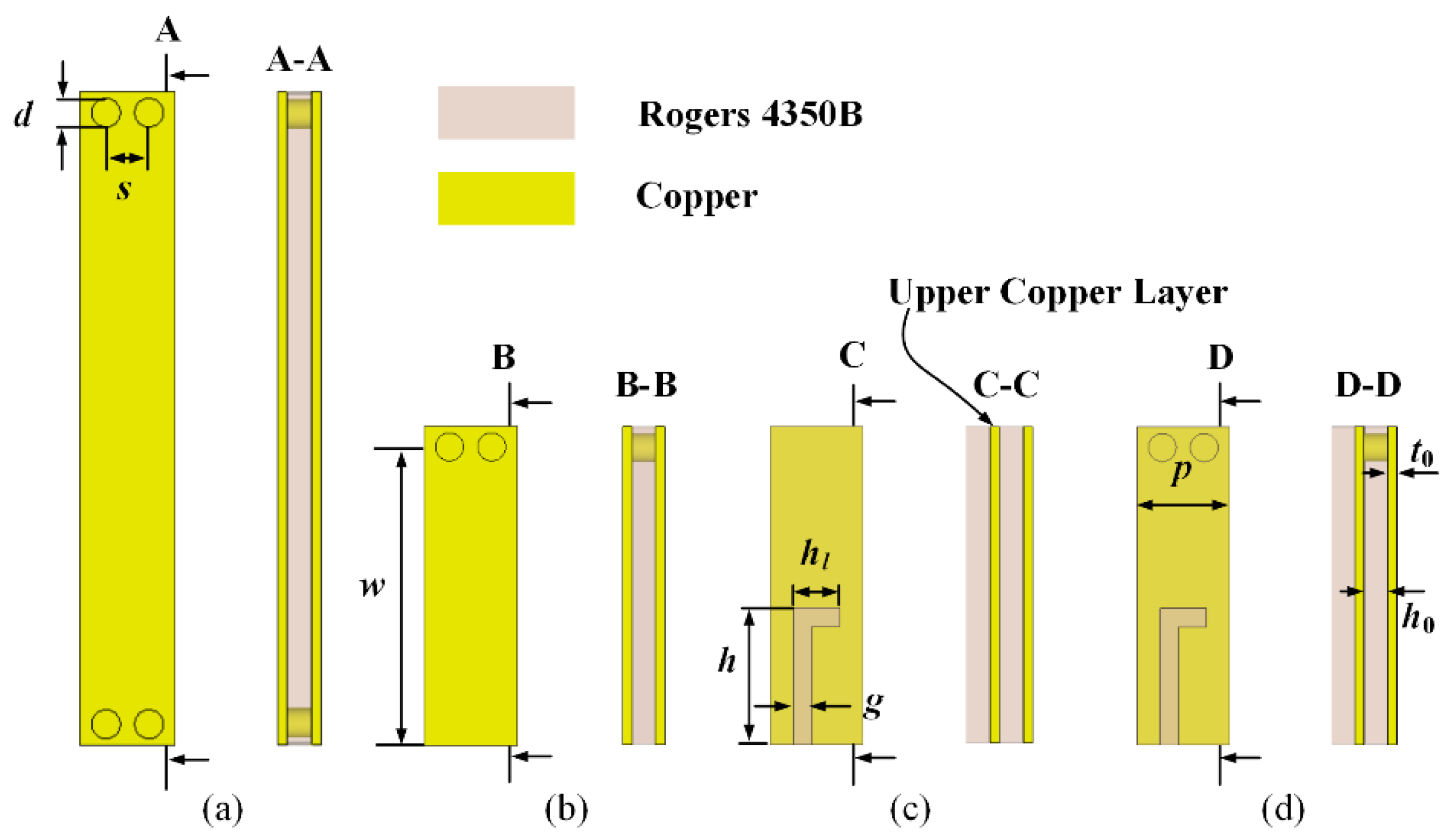
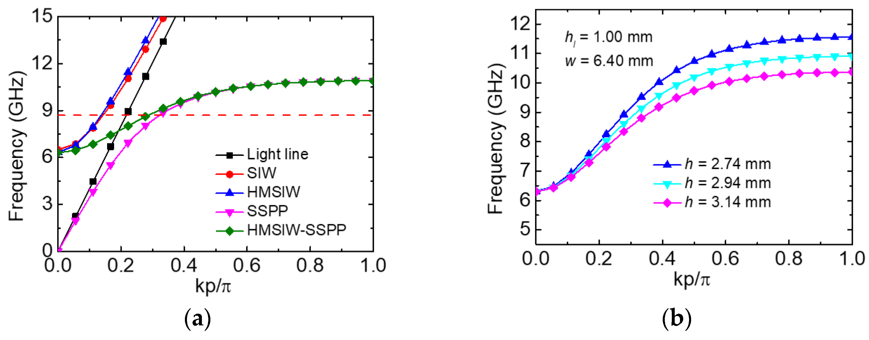
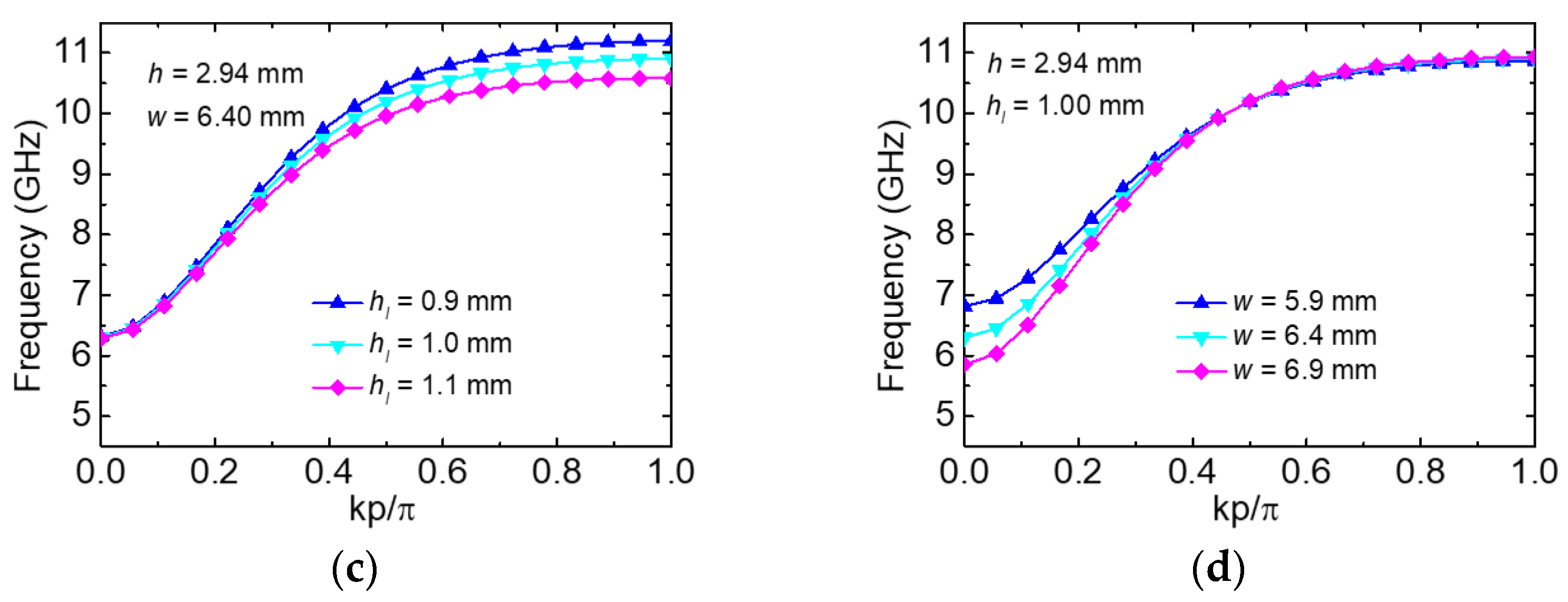
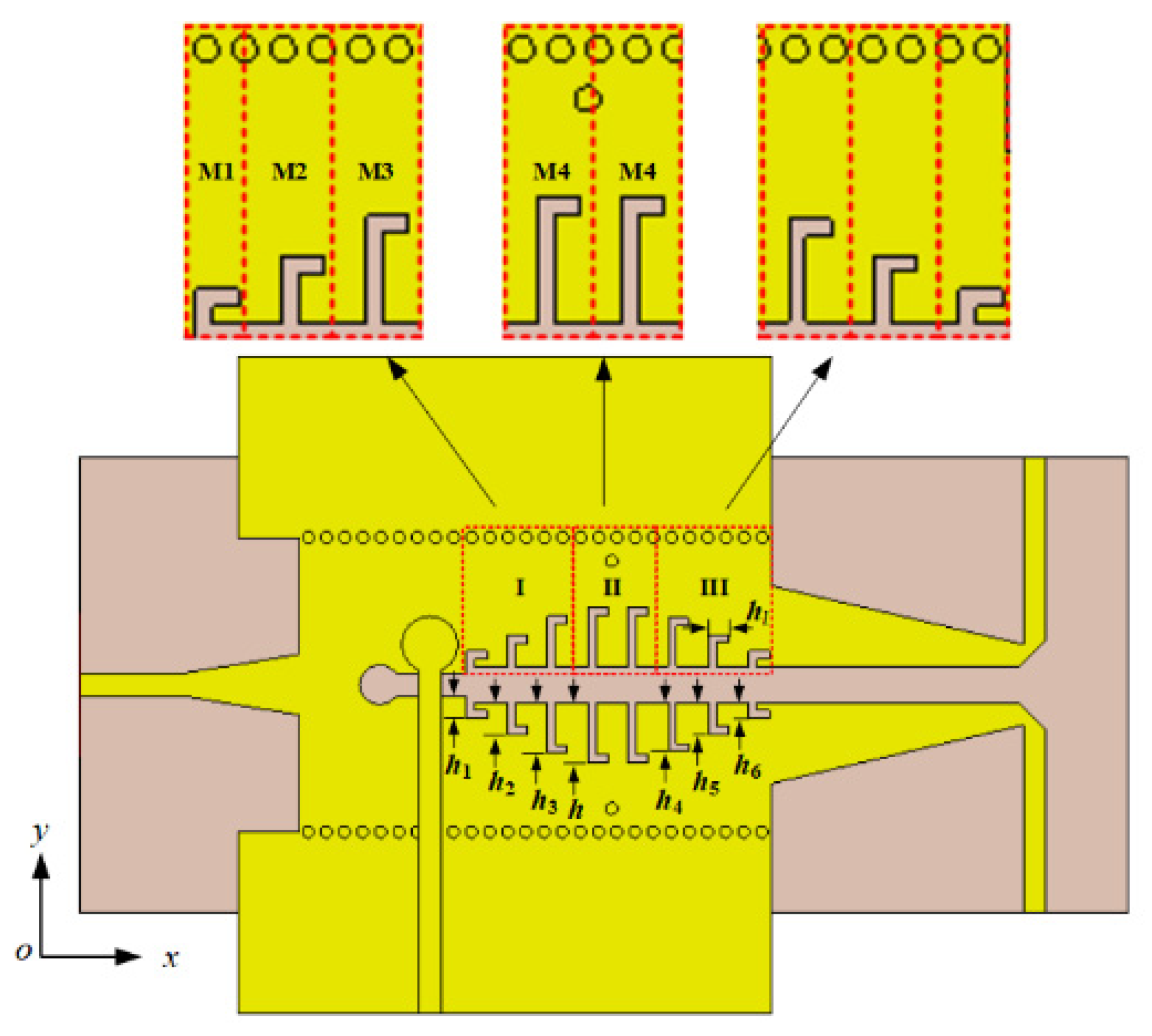
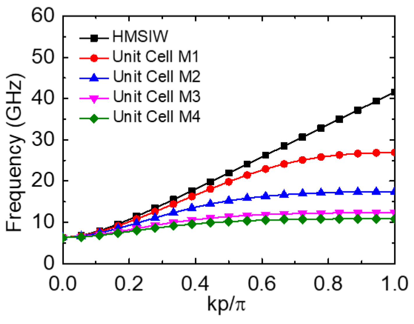
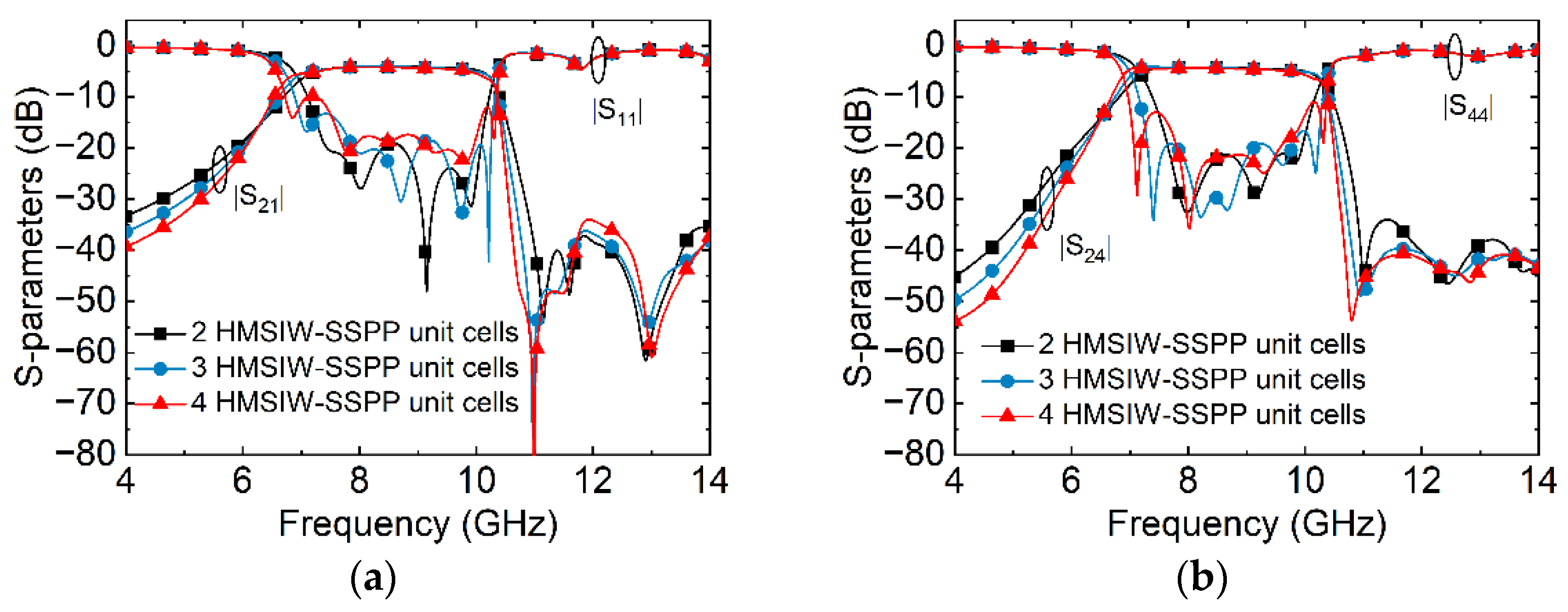
2. Dispersion Characteristics Analysis of Unit Cells
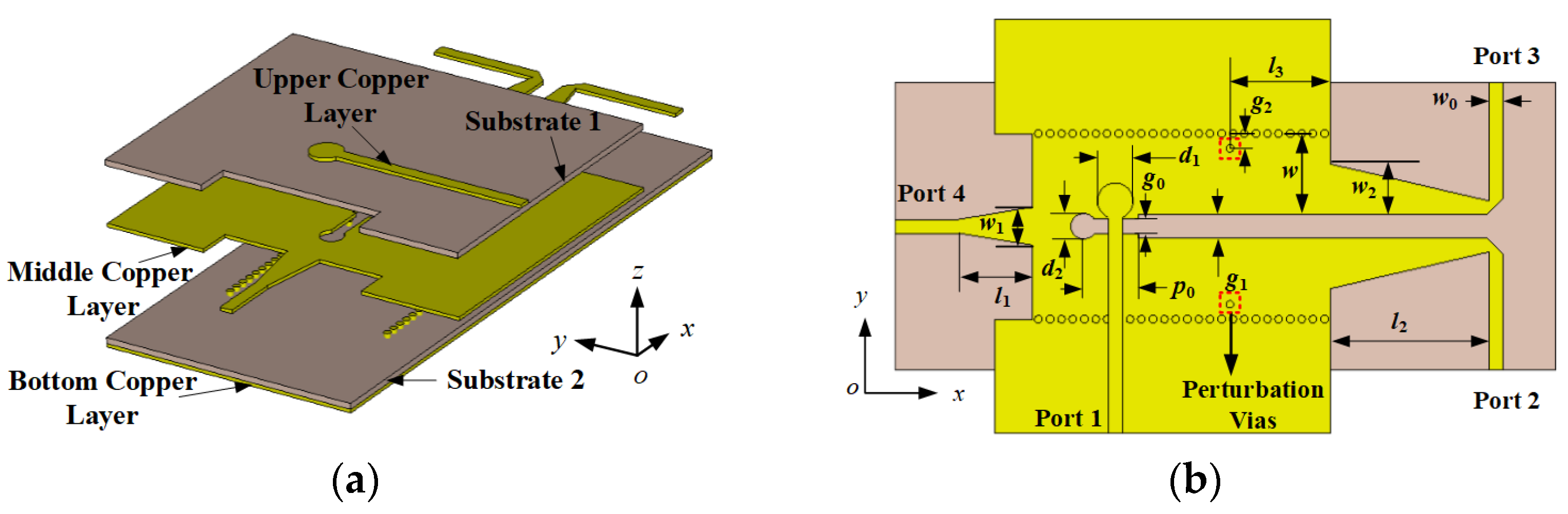
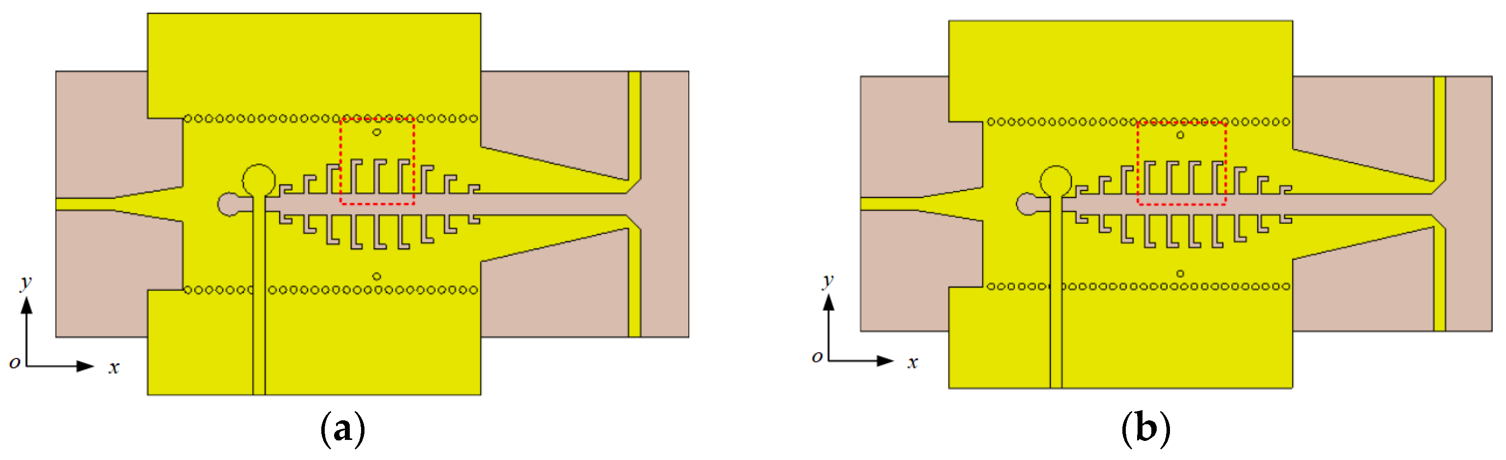
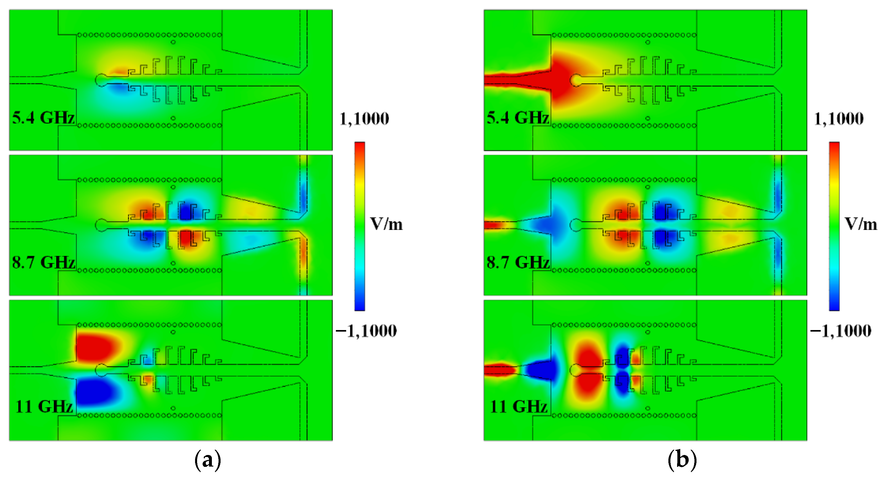
3. Design of HMT
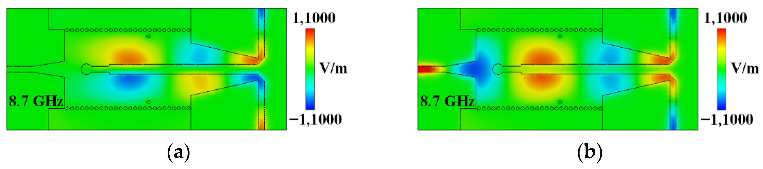
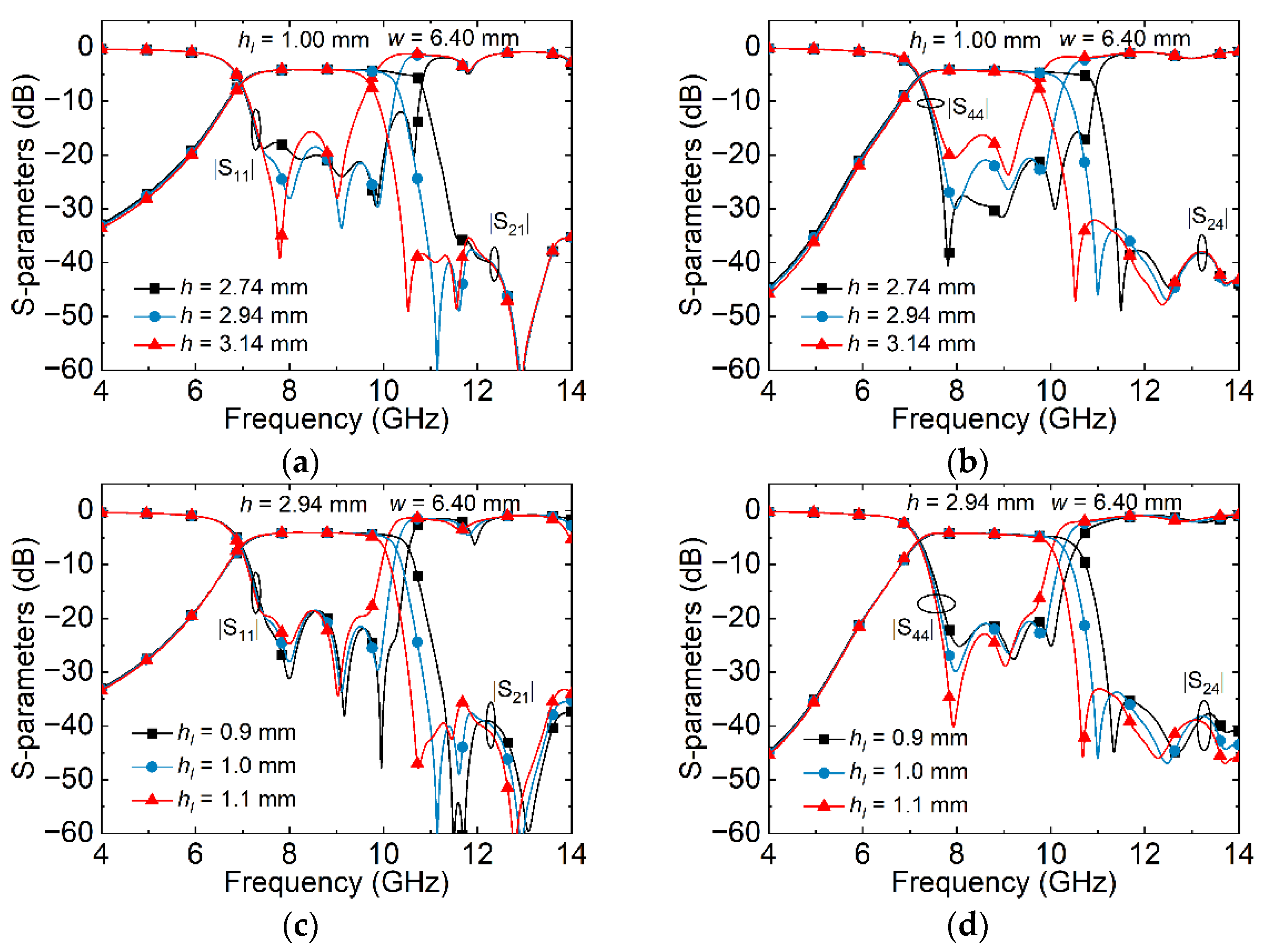
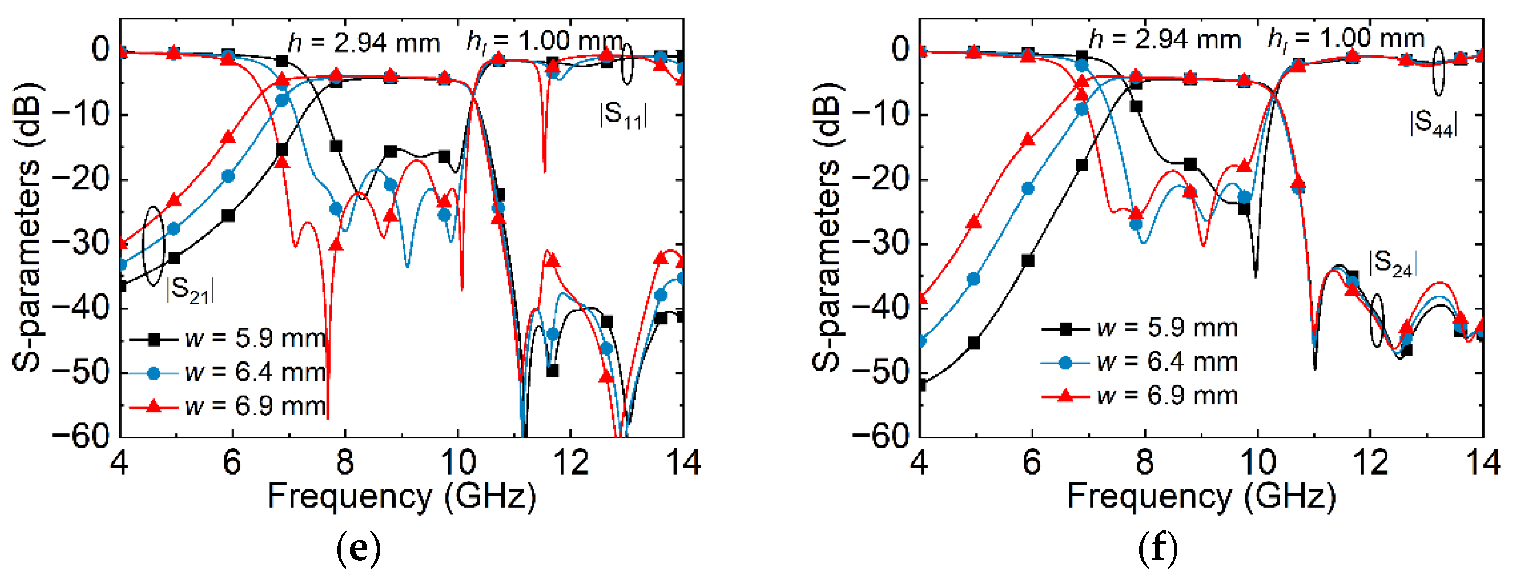
4. Design of FMT
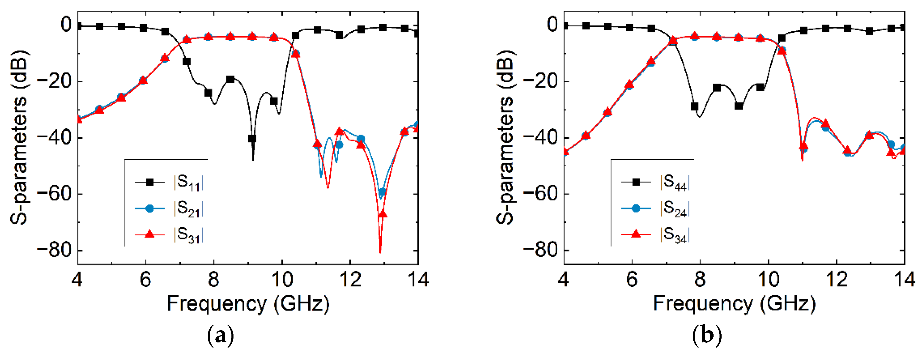
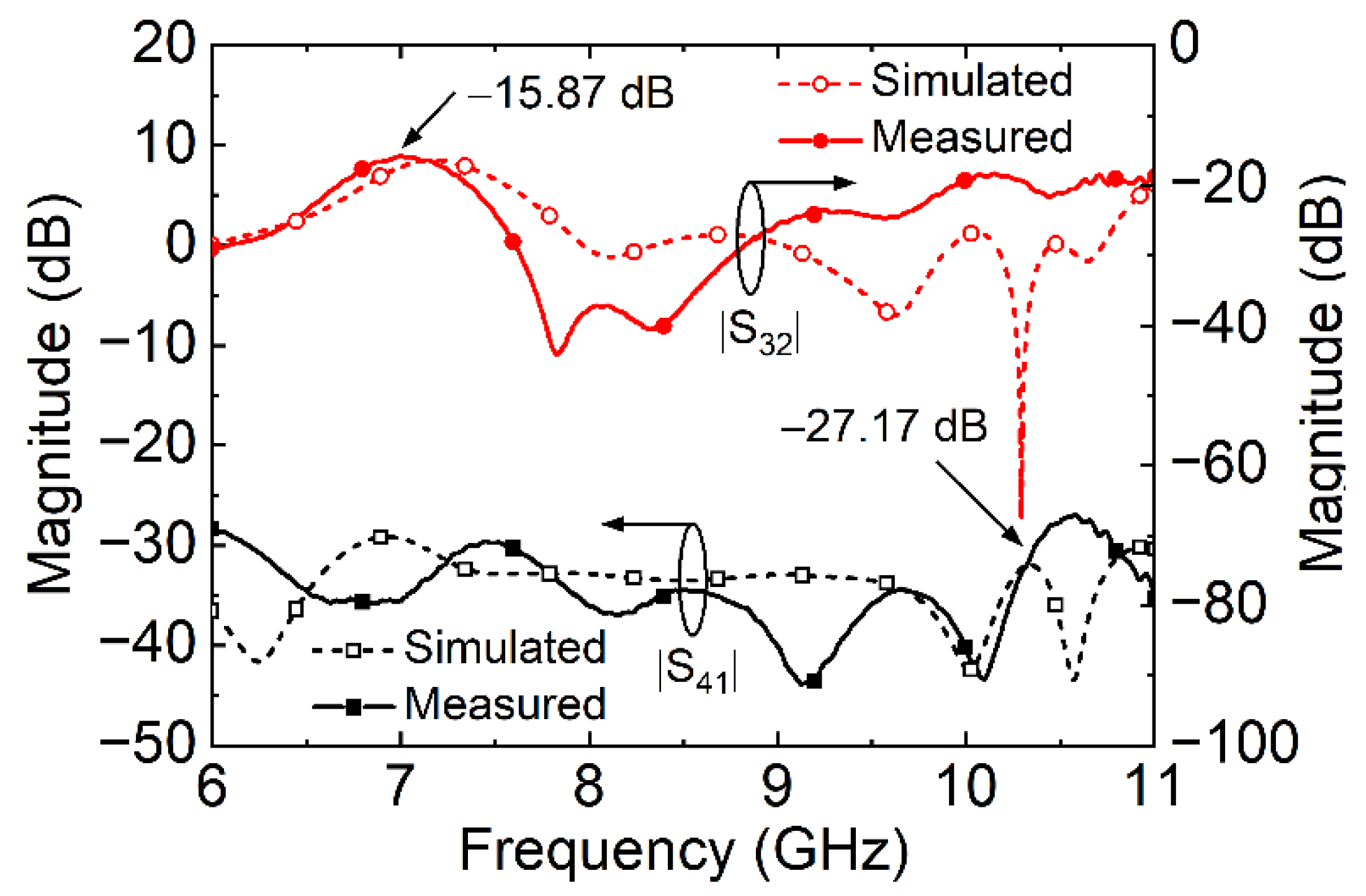
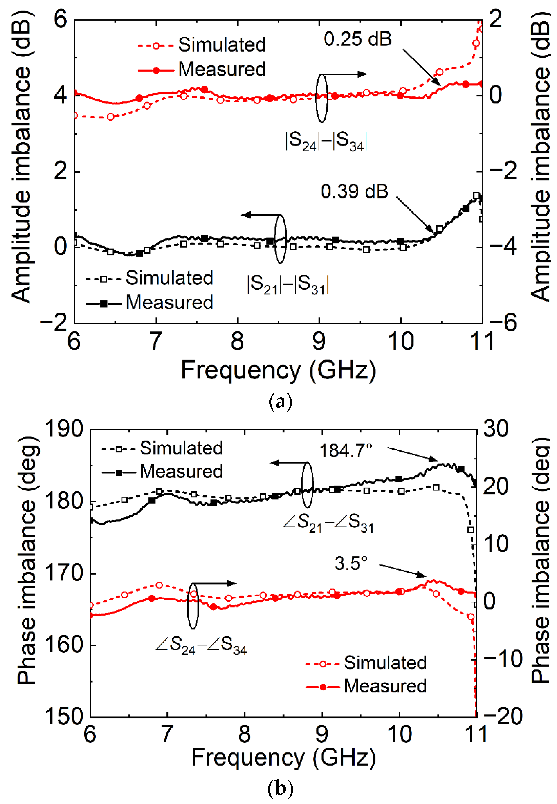
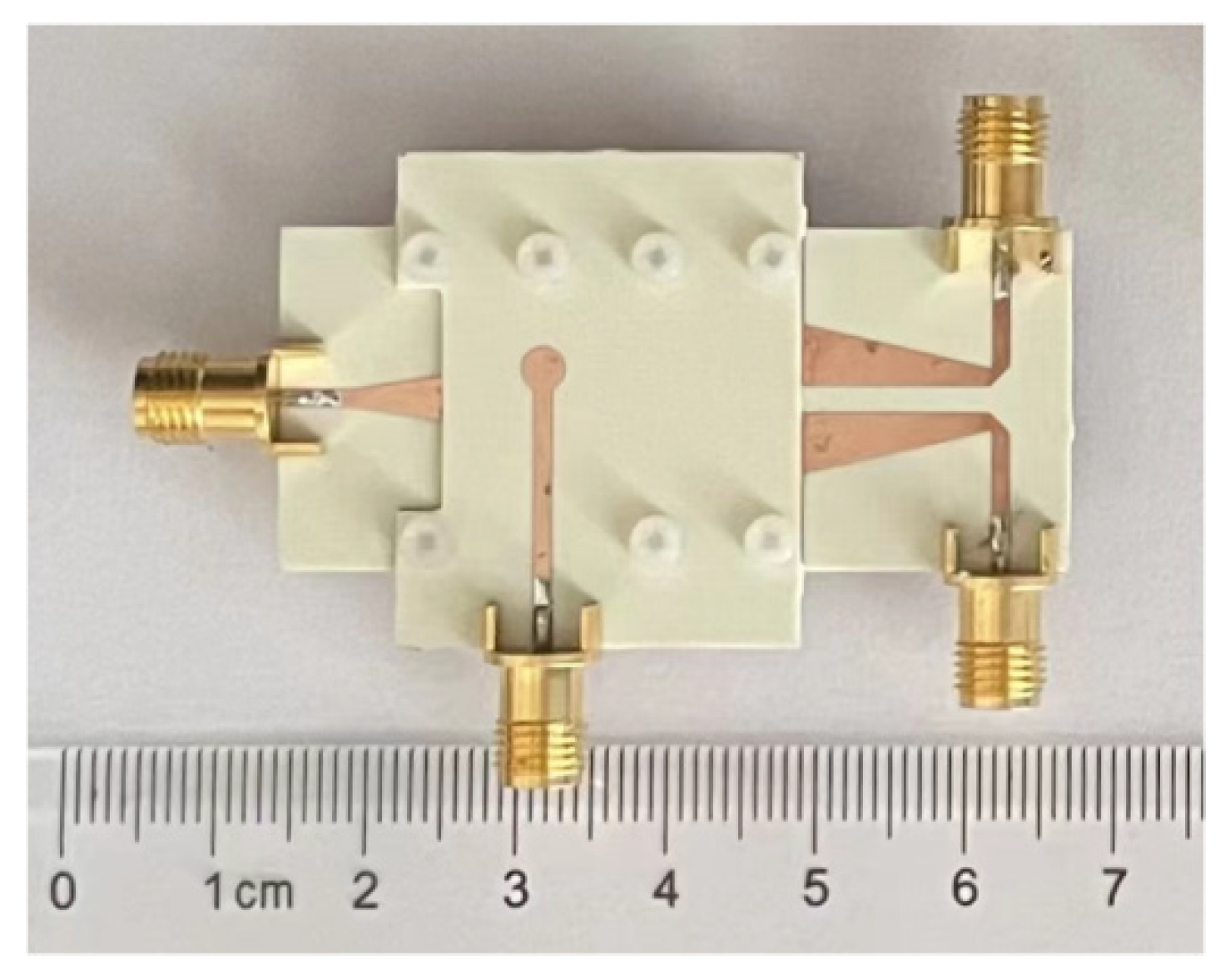
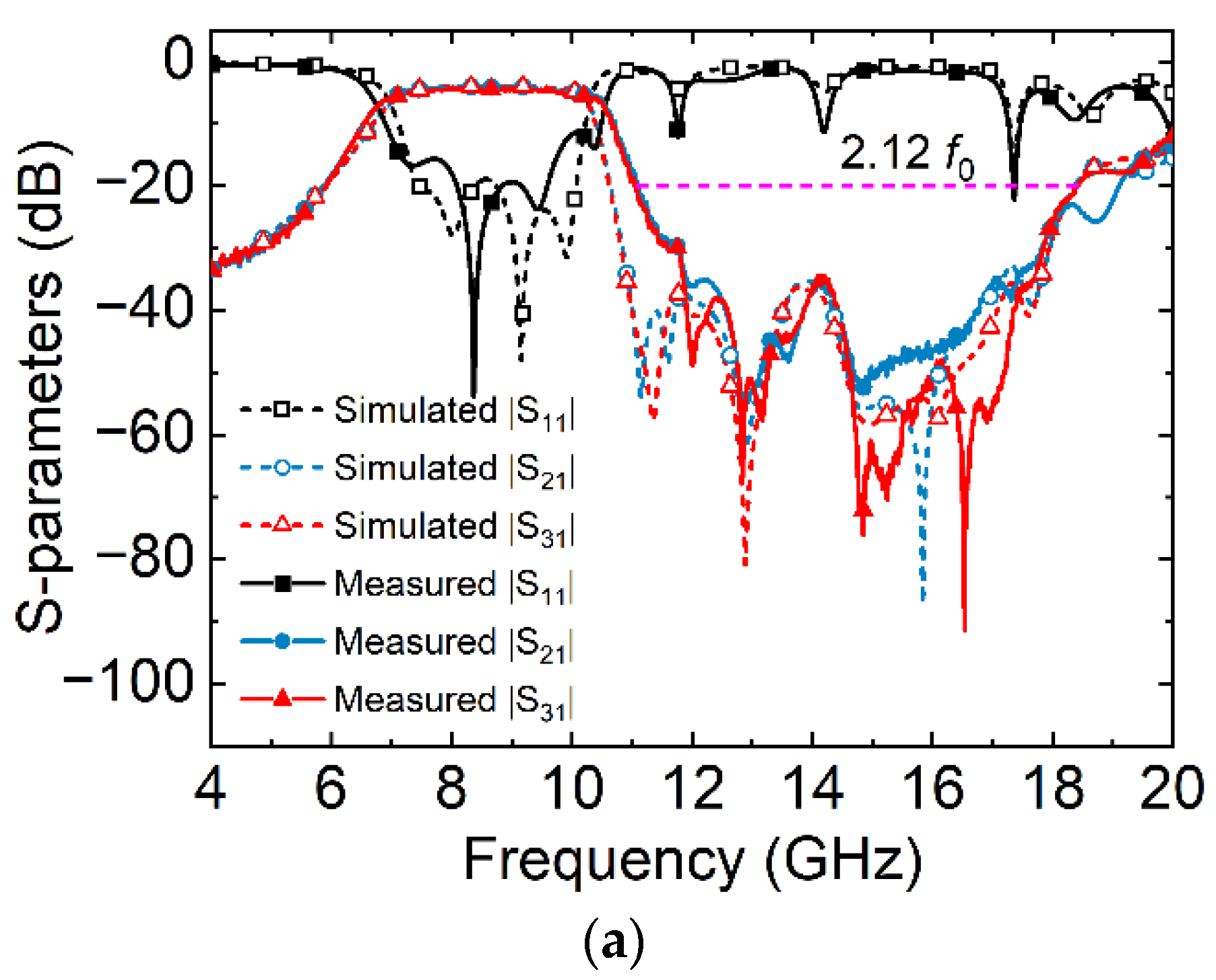
5. Measurement and Discussion
6. Conclusions
Author Contributions
Funding
Data Availability Statement
Conflicts of Interest
References
- He, F.F.; Wu, K.; Hong, W.; Han, L.; Chen, X. A planar magic-T structure using substrate integrated circuits concept and its mixer applications. IEEE Trans. Microw. Theory Tech. 2011, 59, 72–79. [Google Scholar] [CrossRef]
- Nagaraju, D.; Verma, Y.K. A compact wideband planar magic tee for monopulse antenna array applications. IEEE Microw. Wirel. Compon. Lett. 2021, 31, 429–432. [Google Scholar] [CrossRef]
- Huang, G.-L.; Zhou, S.-G.; Chio, T.-H. Highly-Efficient Self-Compact Monopulse Antenna System with Integrated Comparator Network for RF Industrial Applications. IEEE Trans. Ind. Electron. 2017, 64, 674–681. [Google Scholar] [CrossRef]
- He, F.F.; Wu, K.; Hong, W.; Tang, H.J.; Zhu, H.B.; Chen, J.X. A Planar Magic-T Using Substrate Integrated Circuits Concept. IEEE Microw. Wireless Compon. Lett. 2008, 18, 386–388. [Google Scholar]
- Feng, W.; Che, W.; Deng, K. Compact Planar Magic-T Using E-Plane Substrate Integrated Waveguide (SIW) Power Divider and Slotline Transition. IEEE Microw. Wireless Compon. Lett. 2010, 20, 331–333. [Google Scholar] [CrossRef]
- Zhu, F.; Hong, W.; Chen, J.-X.; Wu, K. Design and Implementation of a Broadband Substrate Integrated Waveguide Magic-T. IEEE Microw. Wireless Compon. Lett. 2012, 22, 630–632. [Google Scholar] [CrossRef]
- Mansouree, M.; Yahaghi, A. Planar Magic-Tee Using Substrate Integrated Waveguide Based on Mode-Conversion Technique. IEEE Microw. Wireless Compon. Lett. 2016, 26, 307–309. [Google Scholar] [CrossRef]
- Shen, T.-M.; Huang, T.-Y.; Chen, C.-F.; Wu, R.-B. A Laminated Waveguide Magic-T with Bandpass Filter Response in Multilayer LTCC. IEEE Trans. Microw. Theory Tech. 2011, 59, 584–592. [Google Scholar] [CrossRef]
- Li, P.; Chu, H.; Chen, R.S. SIW magic-T with bandpass response. Electron. Lett. 2015, 51, 1078–1080. [Google Scholar]
- Li, H.-Y.; Xu, J.-X.; Zhang, X.Y. Substrate Integrated Waveguide Filtering Rat-Race Coupler Based on Orthogonal Degenerate Modes. IEEE Trans. Microw. Theory Tech. 2019, 67, 140–150. [Google Scholar] [CrossRef]
- Zhang, G.; Zheng, J.; Zhang, X.Y.; Yang, H.; Tang, W.; Yang, J. Dual-Band Balanced to Unbalanced Multilayer Filtering Magic-T Based on SIW Cavity. IEEE Microw. Wireless Compon. Lett. 2022, 32, 387–390. [Google Scholar]
- Cheng, Y.J.; Fan, Y. Compact substrate-integrated waveguide bandpass rat-race coupler and its microwave applications. IET Microw. Antennas Propag. 2012, 6, 1000–1006. [Google Scholar] [CrossRef]
- Rosenberg, U.; Salehi, M.; Bornemann, J.; Mehrshahi, E. A Novel Frequency-Selective Power Combiner/Divider in Single-Layer Substrate Integrated Waveguide Technology. IEEE Microw. Wireless Compon. Lett. 2013, 23, 406–408. [Google Scholar] [CrossRef]
- Zhang, Z.G.; Cheng, Y.J.; Fan, Y.; Zhang, Y.H. Compact substrate integrated waveguide rat-race filtering couplers with arbitrary angular interval between ports. Int. J. RF Microw. Comput.-Aided Eng. 2020, 30, e22168. [Google Scholar] [CrossRef]
- Hagag, M.F.; Khater, M.A.; Sinanis, M.D.; Peroulis, D. Ultra-Compact Tunable Filtering Rat-Race Coupler Based on Half-Mode SIW Evanescent-Mode Cavity Resonators. IEEE Trans. Microw. Theory Tech. 2018, 66, 5563–5572. [Google Scholar]
- Hao, Z.-C.; Ding, W.-Q.; Huo, X.-P. A wideband high selectivity filtering balun. Microw. Opt. Technol. Lett. 2015, 57, 1107–1110. [Google Scholar] [CrossRef]
- Wang, X.; Zong, Z.-Y.; Wu, W. Miniaturized filtering rat-race coupler based on hybrid circular substrate integrated waveguide and coplanar waveguide resonators. Int. J. RF Microw. Comput.-Aided Eng. 2022, 32, e22985. [Google Scholar]
- Shen, S.; Xue, B.; Yu, M.; Xu, J. A Novel Three-Dimensional Integrated Spoof Surface Plasmon Polaritons Transmission Line. IEEE Access 2019, 7, 26900–26908. [Google Scholar] [CrossRef]
- Xu, K.-D.; Zhang, F.; Guo, Y.; Ye, L.; Liu, Y. Spoof Surface Plasmon Polaritons Based on Balanced Coplanar Stripline Waveguides. IEEE Photon. Technol. Lett. 2020, 32, 55–58. [Google Scholar]
- Xu, K.-D.; Guo, Y.-J.; Yang, Q.; Zhang, Y.-L.; Deng, X.; Zhang, A.; Chen, Q. On-Chip GaAs-Based Spoof Surface Plasmon Polaritons at Millimeter-Wave Regime. IEEE Photon. Technol. Lett. 2021, 33, 255–258. [Google Scholar]
- Wang, Z.; Feng, H.; Yang, X.; Xu, X.; Zheng, Y.; Ye, L. A Windmill-Shaped SSPP Waveguide for High-Efficiency Microwave and Terahertz Propagation. Electronics 2022, 11, 1293. [Google Scholar]
- Liu, L.; Liu, Y.; Jin, X.; Li, Z.; Tian, Y. A Broad Dual-Band Bandpass Filter Design Based on Double-Layered Spoof Surface Plasmon Polaritons. Electronics 2022, 11, 697. [Google Scholar]
- Chen, P.; Li, L.; Yang, K.; Chen, Q. Hybrid Spoof Surface Plasmon Polariton and Substrate Integrated Waveguide Broadband Bandpass Filter with Wide Out-of-Band Rejection. IEEE Microw. Wireless Compon. Lett. 2018, 28, 984–986. [Google Scholar]
- Tan, L.; Xu, K.; Liu, Y.; Guo, Y.; Cui, J. Spoof Surface Plasmon Polaritons Developed from SIW Using Ring Slots and Vias. Electronics 2021, 10, 1978. [Google Scholar]
- Yang, Z.-B.; Guan, D.-F.; Zhang, Q.; You, P.; Hou, X.-X.; Xu, S.-D.; Yong, S.-W. A hybrid substrate-integrated waveguide and spoof surface plasmon-polariton one-layer dual bandpass filter formed by resonant tunneling effect. Appl. Phys. Express 2018, 11, 114101. [Google Scholar]
- Lin, Y.; Xiao, B.; Li, X. Dual bandpass filter based on spoof surface plasmon polaritons and half-mode substrate integrated waveguide. Opt. Quantum Electron. 2022, 54, 12. [Google Scholar]
- Pan, B.C.; Yu, P.; Liao, Z.; Zhu, F.; Luo, G.Q. A Compact Filtering Power Divider Based on Spoof Surface Plasmon Polaritons and Substrate Integrated Waveguide. IEEE Microw. Wireless Compon. Lett. 2022, 32, 101–104. [Google Scholar]
- Moznebi, A.-R.; Afrooz, K. Bandwidth enhancement of a half-mode substrate integrated waveguide filtering power divider using spoof surface plasmon polariton. J. Phys. D Appl. Phys. 2021, 55, 025103. [Google Scholar] [CrossRef]
- Cui, Y.; Xu, K.-D.; Guo, Y.-J.; Chen, Q. Half-mode substrate integrated plasmonic waveguide for filter and diplexer designs. J. Phys. D Appl. Phys. 2022, 55, 125104. [Google Scholar]
- Soleimani, S.; Mirhadi, S.; Komjani, N. Design of a broadband diplexer based on substrate integrated plasmonic waveguide. Int. J. RF Microw. Comput.-Aided Eng. 2021, 31, e22854. [Google Scholar]
- CST Microwave Studio. CST Corp.: Darmstadt, Germany. Available online: www.cst.com (accessed on 28 July 2022).
- Yang, Z.-B.; Guan, D.; Zhang, Q.; Xu, H.; Lin, M.; Zhang, X.; Hong, R.; Yong, S.-W. Mode Composite Waveguide Based on Hybrid Substrate Integrated Waveguide and Spoof Surface Plasmon Polariton Structure. IEEE Trans. Circuits Syst. I Regul. Pap. 2021, 68, 1472–1480. [Google Scholar] [CrossRef]
- Hao, Z.C.; Kong, F.F. Developing high performance Q-band planar filters using the multilayered substrate integrated waveguide technique. Microw. Opt. Technol. Lett. 2017, 59, 698–703. [Google Scholar] [CrossRef]
- Zhang, D.; Zhang, K.; Wu, Q.; Jiang, T. A Compact Wideband Filter Based on Spoof Surface Plasmon Polaritons with a Wide Upper Rejection Band. IEEE Photon. Technol. Lett. 2020, 32, 1511–1514. [Google Scholar] [CrossRef]


| Ref. | f0 (GHz) | FBW (%) | IL (dB) | AI. (dB) /PI. (°) | FR | Rej. (dB) /S.B. (f0) | Size (λg × λg) | Tech. Type. |
|---|---|---|---|---|---|---|---|---|
| [4] | 8.9 | 11.24 | 0.7 | 0.2/1.5 | No | - | 3.98 × 2.46 | SIW |
| [5] | 14.5 | 17.93 | 0.43 | 0.23/1.5 | No | - | 4.64 × 2.99 | SIW |
| [8] ⁎ | 24.1 | 8.59 | 2.24 | 0.25/6 | Yes | No. | 1.19 × 1.26 | LTCC |
| [8] ⁑ | 24.25 | 8.62 | 2.2 | 0.25/6 | Yes | No | 1.20 × 1.27 | LTCC |
| [9] ⁎ | 9 | 0.78 | 1.91 | 0.35/5 | Yes | No | 2.44 × 2.44 | SIW |
| [9] ⁑ | 9.01 | 0.78 | 1.91 | 0.35/5 | Yes | No | 2.44 × 2.44 | SIW |
| [10]-1 | 11.8 | 3.4 | 1.3 | 0.1/2.5 | Yes | No | 1.18 × 1.18 | SIW |
| [10]-2 | 10.94 | 3.1 | 1.3 | 0.05/2.5 | Yes | No | 0.88 × 1.64 | SIW |
| [12] | 7.75 | 2.6 | 1.45 | 0.56/5 | Yes | 20/1.48 | 0.79 × 0.42 | SIW |
| [13] | 11 | 1.4 | 2 | 0.8/9 | Yes | No | 1.36 × 1.28 | SIW |
| [14]-1 | 10.3 | 2.7 | 1.4 | 0.05/3 | Yes | No | 1.21 × 1.21 | SIW |
| [14]-2 | 10.2 | 3.1 | 1.35 | 0.1/3 | Yes | No | 1.19 × 1.19 | SIW |
| [17] | 10.02 | 7.58 | 0.89 | 0.48/4.8 | Yes | No | 1.22 × 1.22 | SIW-CPW |
| T.W. ⁎ | 8.7 | 40.23 | 1.09 | 0.39/4.7 | Yes | 20/2.12 | 2.81 × 1.76 | HMSIW-SSPP |
| T.W. ⁑ | 8.83 | 38.96 | 1.27 | 0.39/4.7 | Yes | 20/2.08 | 2.85 × 1.79 | HMSIW-SSPP |
Publisher’s Note: MDPI stays neutral with regard to jurisdictional claims in published maps and institutional affiliations. |
© 2022 by the authors. Licensee MDPI, Basel, Switzerland. This article is an open access article distributed under the terms and conditions of the Creative Commons Attribution (CC BY) license (https://creativecommons.org/licenses/by/4.0/).
Share and Cite
Liu, H.; Xue, B.; Xu, J. Design of Filtering Magic-T with Wideband and Wide Stopband Based on HMSIW and Spoof Surface Plasmon Polaritons. Electronics 2022, 11, 2699. https://doi.org/10.3390/electronics11172699
Liu H, Xue B, Xu J. Design of Filtering Magic-T with Wideband and Wide Stopband Based on HMSIW and Spoof Surface Plasmon Polaritons. Electronics. 2022; 11(17):2699. https://doi.org/10.3390/electronics11172699
Chicago/Turabian StyleLiu, Hao, Bing Xue, and Jun Xu. 2022. "Design of Filtering Magic-T with Wideband and Wide Stopband Based on HMSIW and Spoof Surface Plasmon Polaritons" Electronics 11, no. 17: 2699. https://doi.org/10.3390/electronics11172699
APA StyleLiu, H., Xue, B., & Xu, J. (2022). Design of Filtering Magic-T with Wideband and Wide Stopband Based on HMSIW and Spoof Surface Plasmon Polaritons. Electronics, 11(17), 2699. https://doi.org/10.3390/electronics11172699