Abstract
A broadband GaN MMIC power amplifier (PA) with compact dimensions of 1.94 × 0.83 mm2 is presented for 5G millimeter-wave communication. To guarantee output capability at the operating band edges where serious performance degradation is likely to occur, the appropriate large-signal matching model and optimal impedance domain need to be carefully determined through load-pull analysis. Broadband matching networks (MNs) in the lowpass form are thereafter developed based on the Chebyshev filter synthesis theory. Using high-pass interstage MN in conjunction with parallel RC lossy circuits to compensate for the transistor’s negative gain roll-off slope ensures a flat frequency response. The input MN is designed as a band-pass filter due to the reactance extracted from the input side of the stabilized device exhibiting series LC resonance characteristics. Measured on-wafer pulsed results for the proposed three-stage PA demonstrate up to 30.9 dBm of output power, more than 28.6 dB of small-signal gain, and a peak power-added efficiency (PAE) of 35.6% at 27 GHz. Both uniform gain and saturated output power (Psat) are achieved across 24–30 GHz with fluctuations of less than 0.8 dB.
1. Introduction
The rapid development of smart cities and the popularity of IoT applications have promoted the widespread deployment of commercial 5G networks, which now mainly operate in sub-6 GHz to provide wide-area signal coverage. However, as new standards and advanced services continue to roll out, sub-6 5G will no longer meet future needs because of its limited low-band resources. In contrast, millimeter-wave (mmW) bands not only possess an abundant spectrum to carry massive wireless connections and deliver huge speed improvements but also feature short wavelengths, which are in line with the trends of telecommunication systems toward large bandwidth, low latency, and miniaturization. The 24–30 GHz frequency range covering the overlapping bands n257, n258, and n261 has been the world’s most-utilized 5G mmW spectrum range to date and is attracting extensive attention from researchers. In this context, as a critical building block of the RF front-end, the power amplifier (PA) should have a fractional bandwidth (FBW) of 22% to be compatible with these three bands in order to enhance the integration and reliability of the 5G system while also maintaining good efficiency.
Constrained by the gain–bandwidth product of active devices, proper design strategies need to be adopted to realize a flat gain response and reach a fair compromise between efficiency and output power (Pout) over the expected frequency range. According to the target level, the mainstream broadband schemes for PAs reported in the most recent literature can be roughly divided into three categories. In the architecture aspect, the major ones are distributed, balanced, and differential amplifiers that are capable of achieving more than a one-octave bandwidth via artificial transmission lines, 3 dB couplers, and balun transformers, respectively [1,2,3]. However, they generally have the evident drawback of bulky size, and some of them could suffer from significant losses or poor efficiency, restricting their use to certain scenarios. Circuit-level methods can be summarized as the parameter solution for matching networks (MNs), among which the simplified real frequency technique (SRFT), based on numerical analysis, utilizes a programmed optimization algorithm to find the network with maximum transducer power gain [4,5]; however, this necessitates the iterative modification of the independent variables to attain global convergence. An analytical approach to filter synthesis allows the construction of MNs with specified bandwidths and suitable passband types depending on the load composition; moreover, complete closed-form solutions can be obtained for simple loads such as RC, RL, or RLC [6,7,8,9,10], making them more flexible and easier to apply compared to the computationally intensive SRFT. As for the device level, negative feedback and reactive/resistive matching effectively alleviate the gain roll-off characteristics of transistors, which offer considerable advantages in terms of cost, space, and complexity [11,12,13,14]. From another perspective, reducing the impedance transformation ratio (ITR) of MN is also a valid way to extend the bandwidth. As a representative of third-generation wide-bandgap semiconductors, gallium nitride (GaN) has a higher breakdown electric field, saturated electron drift velocity, and thermal conductivity than Si and GaAs materials; thus, GaN-based devices have outstanding performance in power density, cutoff frequency (fT), and temperature resistance [15,16,17]. Meanwhile, their inherent large output resistance, along with small parasitic capacitance, helps to lower ITR without the need for a cascode or stacked configuration, commonly used in CMOS technology [18]. There is no doubt that a GaN high-electron-mobility transistor (HEMT) is the ideal candidate for broadband high-efficiency mmW PA design.
This paper presents a comprehensive procedure for developing a small-scale 1-watt GaN MMIC PA covering the range of 24–30 GHz. On the basis of the derived optimal load impedance and large-signal matching model, two Chebyshev low-pass networks were synthesized for matching at the last stage to yield a balanced Pout and reasonable efficiency. Parallel RC lossy networks were employed to stabilize the transistors together with a high-pass MN at every stage to equalize the overall frequency response without sacrificing too much gain. A band-pass filter was designed using closed-form solutions to improve the input return loss over broadband. The proposed PA was fabricated in OMMIC’s 0.1 μm GaN-on-Si process, known as D01GH [19]. The experimental results are summarized and compared to those from previously published studies.
2. Circuit Design Considerations
2.1. Choice of Amplifier Topology and Transistor Size
In consideration of the mismatch, transmission loss, process variation, and maximum available gain (MAG) of transistors, a cascaded, three-stage, common-source architecture was employed to achieve a small-signal gain above 26 dB. Next, the unit cell periphery needed to be chosen carefully. Although the larger transistor delivers a higher Pout, the lower optimal impedance complicates broadband matching, resulting in higher loss. Moreover, additional parasitics will decrease both the fT and the maximum oscillation frequency (fmax), leading to elevated energy consumption and a deteriorated PAE. Therefore, the total gate width (TGW) of the output stage cell should be set to be smaller under the premise of fulfilling 1 W Psat, which is estimated to be 370 μm when given a 1.25 dBm trade-off margin with a moderate RF power density of 3.6 W/mm. There are three combinations for power cell implementation according to a unit gate width (UGW) ≤ 100 μm and a number of gate fingers (NGF) ≤ 8 being recommended in the foundry design manual for model accuracy reasons. Since the signal travels along the gate with a steady rise in attenuation and phase shift, and on account of phase differences between the gate fingers, excessive UGW and NGF will both cause a reduction in the forward gain. Table 1 reveals that cells with a minor UGW have better frequency response characteristics for similar TGWs, and the terminal impedances of these cells at the center frequency (f0) are fairly close to one another. As a result, the eight-finger HEMT was chosen, and the former ones were subsequently settled following a conservative staging ratio of 1:2. Regarding the soft compression phenomena of GaN-based devices, the first stage cell was slightly enlarged to 50 × 2 μm to enhance the linear driving capability, which seldom impacts the final PAE. The overall class-AB amplifier topology is shown in Figure 1.

Table 1.
Simulated fT, fmax, and the terminal impedances of three unit cells with different fingers but similar TGWs (around 370 μm) at the nominal bias conditions of Vds = 12 V and Vgs = −1 V, where the maximum device DC and AC transconductance appear.
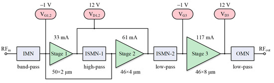
Figure 1.
Block diagram of the proposed multistage power amplifier.
2.2. Stability
Due to the high intrinsic gain, active GaN devices are more prone to self-oscillation and can cause circuit failures. Hence, all selected power cells must be adequately stabilized at the very beginning. Figure 2 presents two typical stabilization measures applied at the transistor’s input to avoid any power loss, where the reactive/resistive lossy MN in the form of parallel RC ensures in-band stability, whereas the series connection of the stabilizing resistor, Rp, and choke inductor, Lp (or microstrip line, TLp), merged into the gate bias branch aims to improve the low-frequency stability, and it behaves similarly to an open circuit for the amplification chain, which can be freely connected to point A or B depending on layout needs. Special attention should be paid to whether the self-resonant frequency (fSR) of the MIM capacitor, Cs, falls within or below the operating band, as the resulting RF short circuit may trigger potential instability, leading the parallel RC network to lose its role in both stabilization and gain equalization. Furthermore, the inevitable electromagnetic (EM) coupling from the surrounding environment will shift the fSR of the Cs to lower frequencies [2], for which we can split the Cs into two identical square-shaped capacitors connected on both sides of the Rs in parallel so that the parasitic inductance of the capacitor plates can be minimized. In addition, the symmetrical layout contributes to the signal transmission consistency and realizes the input balance of the transistor.
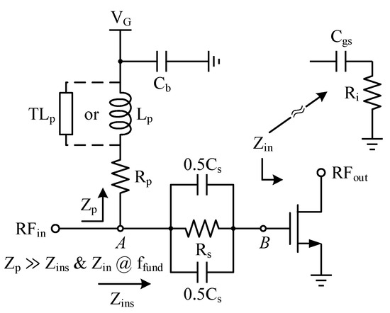
Figure 2.
Schematic of the stabilized transistor.
To quantify the impact of the RC stabilization network on the matching bandwidth, using Equations (1) and (2), the channel resistance, Ri, and the depletion capacitance, Cgs, of the 46 × 8 μm cell are found to be 5.3 Ω and 0.655 pF, respectively, extracted from the S-parameter simulation at f0 (27 GHz) based on the simplified hybrid-π model of a FET [13].
Omitting the negligible Cgd for simplicity, the individual cell is treated as a unilateral two-port network whose input impedance, Zin, translates into a series combination of Ri and Cgs, as depicted in Figure 2. Suppose the input impedance of a HEMT after stabilization viewed from point A is Zins, then:
From Equations (5) and (6), at f0, the quality factor Q of Zin (i.e., Qin) is 1.7, and the Q of Zins (i.e., Qins) will be larger than Qin when (RsCs) > 10−11, meaning that the maximum attainable bandwidth will be reduced after the insertion of a parallel RC network, which may be true for gain concerns. Fortunately, the upper limit of Q is 2.7 according to Q = f0/BW, with a conservatively designed bandwidth of 10 GHz. In fact, there is enough room for us to achieve the desired compromise between stability, bandwidth, and gain under the obtained boundary condition. We finally chose a stabilization network consisting of two identical 0.68 pF capacitors in parallel with a 30 Ω resistor for the output stage cell, with a Qins of 2.24 determined by Equation (4). In addition, by substituting the reactance X slopes of the two curves in Figure 3 at fSR into Equation (7), it is found that the series parasitic inductance represented by the C-R-C structure is reduced by half, from 21.2–9.6 pH, compared to the conventional R-C one, thereby boosting the fSR to 44.6 GHz.
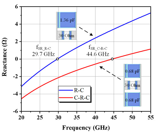
Figure 3.
The reactance of a parallel RC stabilization network.
Figure 4 shows that the Rollett stability factor (K) > 1 is achieved throughout nearly the whole band at the expense of less than 0.9 dB of gain loss. Despite the instability still existing at frequencies below 1 GHz, this problem is solved naturally when considering the losses and filtering functions of all passive networks.
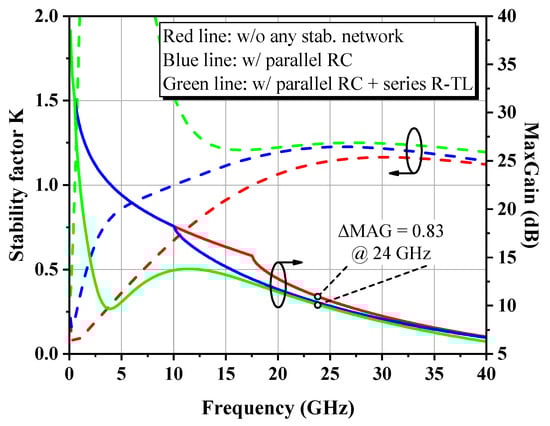
Figure 4.
Simulated K-factor and MAG of the 46 × 8 μm GaN transistor, with and without stabilization networks.
2.3. Load-Pull Analysis and Optimal Impedances Selection
Achieving the continuous and accurate matching of frequency-dependent impedance over broadband is a challenge. On top of that, the designed band usually deviates from evaluation to a lower frequency after implementation, and severe performance degradation tends to happen near the operating band edges, especially at the upper-frequency corner, where gain roll-off issues are highlighted. Therefore, the single-tone load-pull procedures of the stabilized 46 × 8 μm cell were carried out at 24 GHz, 28 GHz, and the extended corner of 32 GHz, while the input was terminated on the conjugate matching condition to determine the tolerance zone, satisfying the preset goal of PAE ≥ 40% and P1dB ≥ 31 dBm to secure the specifications safely. Harmonic control was deliberately neglected since it complicates the MN, and the higher-order harmonic components are far from a passband that can be readily filtered out. From Figure 5a, we can observe that, due to the nonlinear output capacitance, Cout, both the PAE and P1dB contours for load impedances move counterclockwise and narrow with increasing frequency, with the PAE contour shrinking more dramatically, indicating that Cout’s effect on PAE is significant at high frequencies and that the optimal impedance domain defined by the overlapping portion (shaded) of the three sets of contours is primarily bounded by the contours at 32 GHz. Consequently, we chose 11 + j13 Ω as the optimal center load impedance, ZL,opt, close to the impedance points with maximum PAE at high fundamentals. In this way, a wider bandwidth can be produced by intentionally introducing a certain degree of mismatch on the low-frequency side while the high-frequency performance is strengthened.
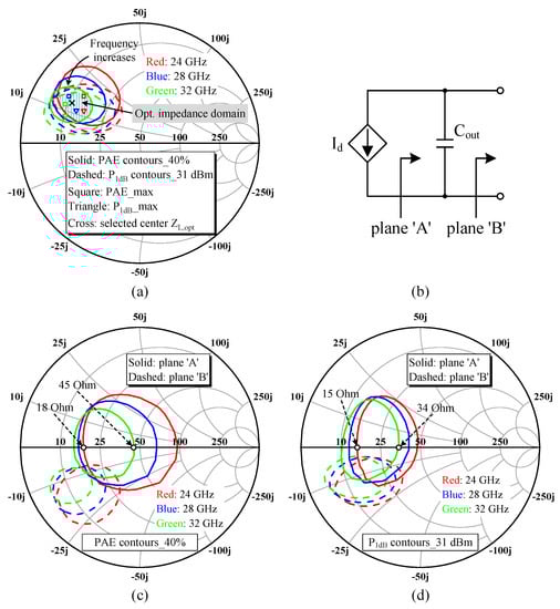
Figure 5.
(a) Load-pull simulations at 1 dB gain compression. (b) Reference planes for the equivalent circuit of the transistor. (c,d) Extracted PAE and P1dB contours at plane ‘A.’
For subsequent analyses and the design of broadband MNs, we needed to derive the parallel RoutCout model for the large-signal output impedance of the cell, in which the extraction of Cout is particularly vital. Assume that the load-pull simulation is performed at the transistor’s internal current source, i.e., reference plane ‘A’ in Figure 5b; the resulting contour will become frequency-independent regardless of any parasitic reactance, and its center will fall on the real axis of the Smith chart, implying that the ideal closed contour will be bisected by the real axis [20]. Based on this conclusion, we can use Equation (8) to calculate the shunt capacitance, Cp, corresponding to the conjugate of ZL,opt and take it as an initial guess for Cout (0.26 pF @ 28 GHz); then, we can try de-embedding different Cout values from the load-pull contours derived at plane ‘B’ one by one in steps of 0.01 pF. When the extracted efficiency and power contours are shifted back to the position symmetrical to the real axis [18], as illustrated in Figure 5c,d, the Cout is identified to be 0.27 pF. Additionally, the acceptable load resistance RL ranges between 18 and 34 Ω.
Since impedance matching must comply with the Bode–Fano criterion and RL is much smaller than the HEMT’s output resistance 1/Gds, we have
Under a known bandwidth, Δω, and Cout, the chosen RL should be as small as possible to minimize the reflection coefficient, |Γm|, but this will increase the ITR and is not beneficial for achieving uniform broadband output performance; thus, we compromised by setting RL to the range’s median value: 26 Ω.
For the input stage device, the priority of which is to provide sufficient driving power, the preferred ZL,opt was selected through a simultaneous conjugate matching simulation so that the device could obtain excellent power gain within the target band. Table 2 lists the optimal load impedance of each stage as well as the output parallel RC model parameters extracted from the load-pull simulations.
Table 2.
Optimal load impedances and the values of large-signal output matching models.
3. Design and Implementation of Matching Networks
3.1. Low-Pass OMN Synthesis and Mixed-Element Implementation
Designing a wideband output matching network (OMN) should consider not only in-band matters but also suppress harmonic distortion. Herein, we adopted a low-pass filter structure that provides a Chebyshev impedance match. On the other hand, bearing in mind that the discontinuity interaction and mutual coupling between adjacent elements will obviously affect the frequency response of compact MNs at mmW, while rigorous EM simulation is extremely time-consuming yet essential, the schematic design was alternated with layout replacement to lessen the risk of unmitigated performance deviations and laborious adjustments when cascading all of them into a complete amplifier.
To start with, the influence of the L-type MN composed of a 1.8 pF DC-block capacitor and the parasitic shunt capacitor of the RF signal pad on an external 50 Ω load at both the input and output terminations was compensated by a high-impedance microstrip line to 48 Ω at 27 GHz. At least two sections of the LC ladder are needed for the Chebyshev filter-based OMN to achieve a transformation ratio of 4.4:1 throughout the target band with a passband ripple less than 0.1 dB, as expressed theoretically in [6]. To facilitate the determination of the normalized g elements through the look-up table, we set the impedance transformation ratio, r, as 4 and the FBW as 0.4 to ensure a sufficient design margin. The generated fourth-order low-pass prototype shown in Figure 6a can be converted into a specific network by inverse normalization Equations (10) and (11).
where Rload and ω0 refer to the desired terminal resistance and center angular frequency, respectively. The preliminarily obtained real-to-real network scaled from 48 Ω to an intermediate impedance of 12 Ω was then turned into a real-to-complex network to finalize the broadband matching to our desired ZL,opt with the automatic optimizer in Advanced Design System (ADS) [8]. Figure 6b shows the resulting MN with the element values listed in Table 3.
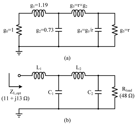
Figure 6.
Two-section low-pass MN: (a) normalized prototype; (b) real-to-complex impedance transformer.
Table 3.
Design parameters for the low-pass OMN.
Considering the feasibility of physical implementation and layout convenience, we directly employed MIM capacitors instead of low-impedance stubs or fan-shaped branches paired with microstrip lines to approximate the ideal lumped elements in the synthesized circuit to construct a mixed-element network. The inductors were replaced by transmission-line sections with a high characteristic impedance, Z0, and a short electrical length, θ, the equivalent series reactance, X, of which is roughly linear to ω, that is:
Narrow microstrip lines were applied in the design to reduce the footprint. Except for the line width in OMN, which is 15 μm, the rest are 10 μm. The supply traces of drain bias and OMN used a double-layer metal to sustain higher current densities and reduce ohmic loss, respectively. In addition, to prevent discontinuity during bending, 45-degree microstrip lines with perpendicular access lines were adopted at the corners.
Figure 7 shows that the input reflection coefficient of OMN rotates clockwise with increasing frequency in the previously determined optimal impedance domain and forms a knot at 24–31.5 GHz, while the second harmonic impedance varies along the periphery of the Smith chart. Moreover, the impedance at 32 GHz highly coincides with ZL,opt, which guarantees the PAE level at high frequencies.
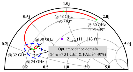
Figure 7.
Simulated S11 of OMN in EM layout format.
3.2. Source-Pull Analysis and Low-Pass ISMN-2 Synthesis
Since the input and output impedances of the cell are somewhat correlated, reacquiring the optimal source impedance, ZS,opt, when loaded with the established OMN allows the cell to run in a better state. It should be mentioned that an even-order harmonic short circuit composed of open and shorted λ/8 stubs with the same characteristic impedance, Z1, in parallel was used as the gate bias for the 46 × 8 μm cell described in Figure 8. The equivalent input impedance, , at the central node, a, can be expressed as Equation (13), which indicates that the present structure not only has the same function of the conventional quarter-wave short-circuit stub but also greatly improves layout utilization by dividing the lengthy λ/4 line in half and arranging them on the upper and lower sides of the chip.
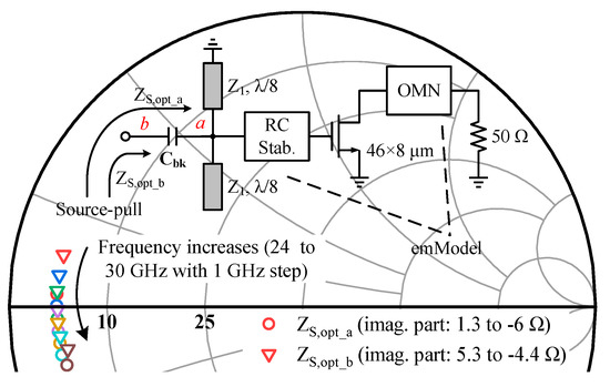
Figure 8.
Optimal input impedances extracted from source-pull simulations.
The source-pull simulations performed at P1dB were repeated within the band of interest at node a to determine the trajectory of ZS,opt_a, as shown in Figure 8, and we noticed they spread across the upper and lower half-planes of the Smith chart. After adding the series 0.73 pF capacitor, Cbk, an updated trajectory with axisymmetric attributes was obtained at node b. The real and imaginary parts of the resulting ZS,opt_b vary within a small range, from 4.4 to 5.2 Ω and from 5.3 to −4.4 Ω, respectively. Hence, the interstage matching network between the second and third stages (ISMN-2) can be regarded as a real impedance transformation from 5 to 75 Ω. Unlike the OMN, where the effect of Cout needs to be canceled out, here, Cout will be exploited to participate in matching, which helps to tackle the design challenge of achieving broadband matching with a large ITR. Likewise, we also referred to the data tabulated in [6], and the Chebyshev low-pass prototype of a 15:1 impedance transformer with 40% FBW was applied and scaled to the 50 Ω system and 27 GHz center frequency in an analogous manner, as illustrated in Figure 9.
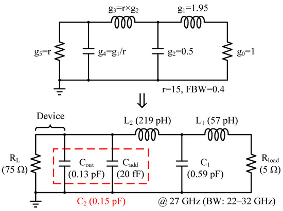
Figure 9.
Conversion from a 0.1 dB equal-ripple low-pass filter prototype to a denormalized network.
After replacing the ISMN-2 into a layout and cascading it with corresponding cells and OMN, we evaluated the total losses associated with each MN, including mismatch and dissipative loss, by injecting a fixed low-power stimulus signal to the interstage cell and calculating the power difference between their input and output ports. The simulation results are displayed in Figure 10. OMN loss increases monotonically in the designed band, with the maximum value not exceeding 1 dB, while the loss curve of ISMN-2 follows a decreasing and then increasing trend, with the valley point located at 29 GHz, and the sum of all losses introduced by both is controlled within the range of 2–2.4 dB. Since the design of the latter two MNs emphasizes achieving better Pout and PAE metrics, compensation for the transistor’s gain roll-off is very limited.
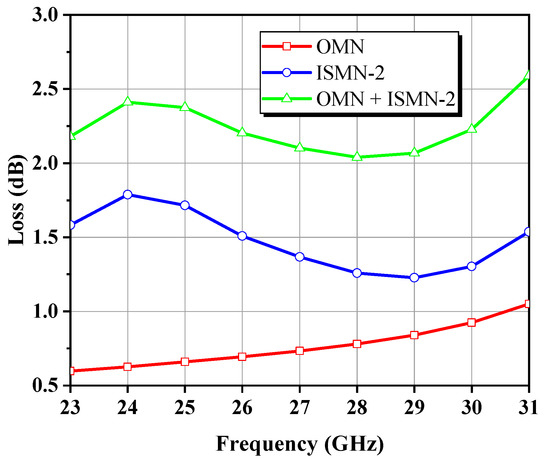
Figure 10.
Estimated total losses for the MNs.
3.3. Compact High-Pass ISMN-1 Design
To dampen the strong low-frequency gain while compensating for the high-frequency response, a two-section high-pass structure was adopted for the interstage matching network between the first and second stages (ISMN-1), and the entire course of impedance transformation was visually proceeded by means of the Smith chart with a constant-Q circle without the extra consideration of DC blocking. The drain feeder was involved in matching to save area. As shown in Figure 11a, Zn (n = 0, 1, …, 5) denotes the impedance looking toward the output end after adding the nth element in sequence. This was determined by Equation (14), where Γn is the simulated reflection coefficient at the terminated 50 Ω reference load connected to the corresponding node, n (blue square). As can be clearly seen from Figure 11b, the impedance profile (Z2–Z5) is rather sensitive to each matching piece, and because of the tight layout of the high-pass network, these elements’ placements and parameters were decided after careful 2.5D EM simulations (ADS Momentum) and comparisons. It is worth mentioning that the value of 4.5 that was chosen to represent the maximum Q is basically defined by the initial Z0, which is equal to the center frequency divided by the required bandwidth. The final curved trajectory, Z5, sandwiches ZL,opt in the middle, creating a knot with a broadband matching nature.
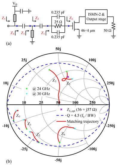
Figure 11.
(a) Schematic of the ISMN-1. (b) Matching trajectory along the ISMN-1 within the 24–30 GHz bandwidth.
3.4. Input Impedance Model and Band-Pass IMN Synthesis
The input impedance, Zin, of the first stage cell with stabilization circuits is plotted in Figure 12a and is represented by the red line. As the frequency increases, Zin moves up along the resistance circle of 12.4 Ω within the range of 26–30 GHz, which can be considered as a series RLC resonant circuit, where the inductance and capacitance values were determined to be 275 pH and 82 fF, respectively. Although this model does not fit well with the variation trends observed in Zin at lower frequencies, owing to irregular changes in the real part of Zin over the band revealed in Figure 12b, it is in good agreement with the imaginary part of Zin, and, as such, we can conclude that LC resonance is the most dominant form of Zin’s reactance.
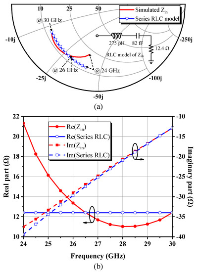
Figure 12.
(a) Simulated S11 of the stabilized 50 × 2 μm cell and series RLC equivalent circuit. (b) Comparison of the real and imaginary parts of Zin and RLC model circuit impedance.
Because the primary objective of the input matching network (IMN) is to improve the return loss in broadband, as long as the reactive component is fully absorbed, the transformation from a designated input impedance to the standard 50 Ω can be achieved precisely, indicating that the best matching topology is the band-pass structure; thus, we adopted closed-form solutions [7] to accomplish the design. Nevertheless, the band-pass network requires twice the number of elements as the low-pass form, a second-order band-pass filter with a target band of 22 to 32 GHz was therefore built to accommodate the practical 6 GHz bandwidth demand. The quality factor, Q, of IMN depends on the series RLC model circuit, which can be obtained from the formula ω0L/R or 1/(ω0RC), where the larger solution result, i.e., Q = 5.9, was taken as the design parameter, and ω0 is the geometric mean angular frequency. The detailed IMN design steps are shown in Figure 13. After the low-pass prototype is derived, each series or shunt element is converted into a band-pass network via resonation at ω0, and Ladd complements the resonant inductance in the model circuit. The Norton transformation acts as an ideal transformer, enabling the up-conversion of RL from 30.3 to 48 Ω without altering the bandwidth. It should be noted that the frequency response represented by Zin and its equivalent model in the low-frequency range of 24–26 GHz demonstrates a relatively large divergence. Hence, the synthesized band-pass network needs to be further tweaked for actual Zin with some sort of compromise.
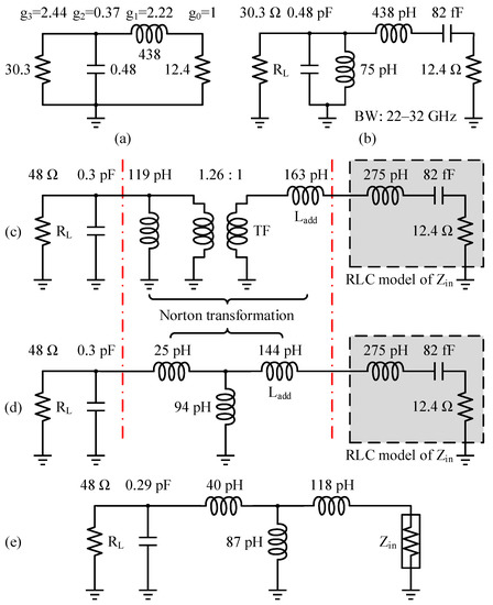
Figure 13.
IMN design flow: (a) low-pass prototype; (b) band-pass version; (c) upward impedance transformation of RL to 48 Ω; (d) Norton transformation to remove the ideal transformer; (e) optimized band-pass network.
Afterward, the stagger-tuning technique was undertaken to optimize the insertion loss of each MN according to their passband properties; the broadband gain response was able to be achieved eventually. To thoroughly check the overall stability of the PA before tape-out, we conducted a series of EM/circuit co-simulations in the wide frequency region from DC to 100 GHz for various possible situations, including different bias voltages and power excitation. The case encountered that μ was less than unity in the 4.9–6.2 GHz range, as shown in Figure 14. Even though the stability of all unit cells was well assured in advance, the shared unilateral supplies, parasitic feedback loops, and coupling effects caused by the compact layout still triggered the formation of new potential instability in the cascaded circuit. Because of this, a 30 Ω resistor, Rb, was added in series with the 3 pF bypass capacitor in both the gate and drain bias paths of the driver stage to eliminate unfavorable oscillations. Figure 15 presents the final schematic of the designed broadband PA.
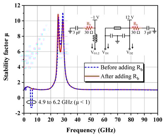
Figure 14.
Stability factor μ before and after adding the Rb.
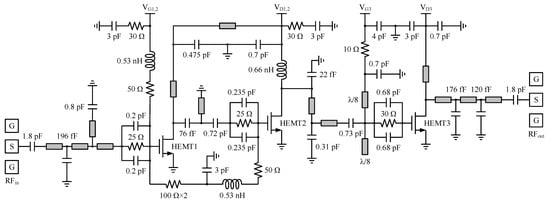
Figure 15.
Complete schematic of the three-stage PA.
4. Measurement Results
Figure 16 shows the proposed MMIC PA fabricated with the industrial 100 nm double heterojunction AlN/GaN/AlGaN HEMT process on a high-resistivity (5 kΩ/cm), 100-μm-thick silicon substrate. Under a 12 V pulsed supply with a 5% duty cycle (200 μs pulse width, 4 ms period) for drains of all stages to avoid overheating during continuous on-wafer testing, as the thermal contact of the chip’s backside on the heat sink is poor, the gate bias voltage was slowly raised from the −1.5 V threshold level until the quiescent current draw reached 211 mA, consistent with the simulation environment.
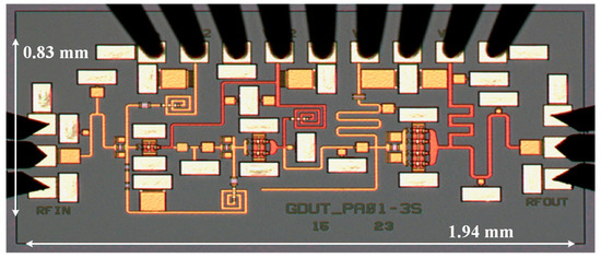
Figure 16.
Die microphotograph of the 24–30 GHz GaN MMIC PA.
4.1. Small-Signal Characterization
After calibrating out the losses of coax cables and GSG probes (150 μm pitch), Figure 17 exhibits that the measured input and output return loss are both greater than 10.5 dB, as well as a linear gain exceeding 28.6 dB over 24–30 GHz with 0.8 dB total variation. The pulsed test outcomes recorded by a vector network analyzer (Keysight N5245A PNA-X) agree nicely with simulations in continuous-wave (CW) mode, with the exception of S21, which is higher than predicted from 23.5 GHz onwards. Moreover, no oscillations arise, and the out-of-band gain drops substantially as intended thanks to the filter-based MNs; such band selectivity eases the later transmitter build-up.
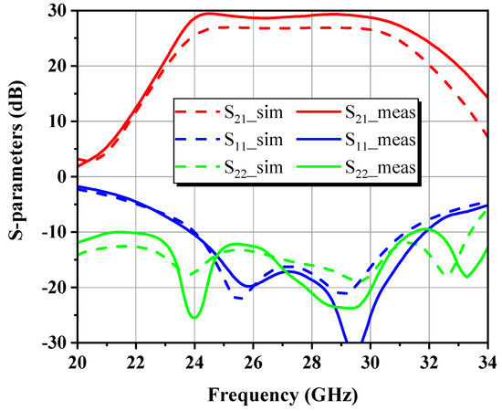
Figure 17.
S-parameters of the proposed PA.
4.2. Large-Signal Characterization
Figure 18 and Figure 19 show that P4dB is beyond 30 dBm, Psat ranges from 30.5–30.9 dBm, and the PAE at P4dB reaches 30.6%–34.7% across the band of interest at room temperature. Power sweep characteristic curves at three discrete frequencies are plotted in Figure 20, where the maximum PAE approaches 35.6% found in the vicinity of P6dB at 27 GHz, and PAE peaks at other frequency points occur at around 4 dB of gain compression. The total current consumption grows to about 288–320 mA when the PA is driven into saturation.
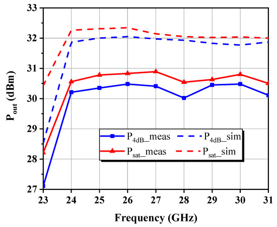
Figure 18.
Measured and simulated Pout at 4 dB gain compression and in the saturation state.
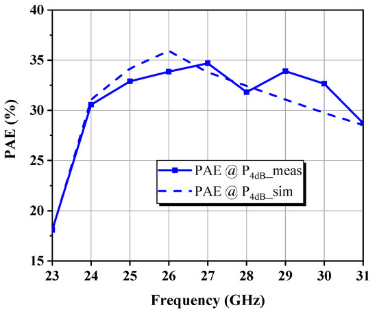
Figure 19.
Measured and simulated PAE at P4dB versus frequency.
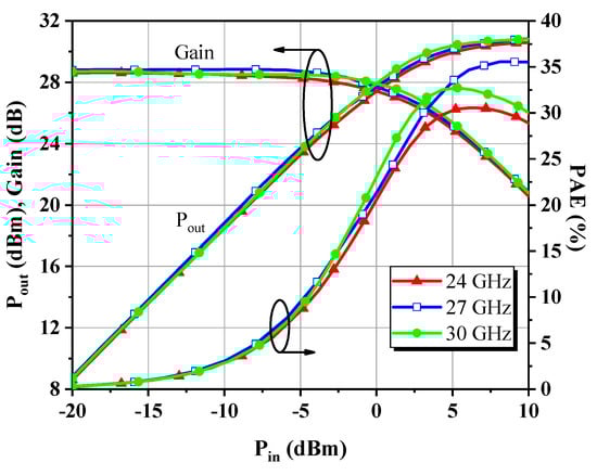
Figure 20.
Measured Pout, PAE, and gain behaviors with respect to input power at 24, 27, and 30 GHz.
The discrepancies between the measured and simulated data mainly come from the accuracy of the transistor nonlinear electro-thermal model, self-heating from the finger dissipation, manufacturing errors in MIM capacitors, and the quality of the probe card contact. The experimental performances are summarized and compared to previously reported GaN PAs with similar frequency bands in Table 4.
Table 4.
Performance summary and comparisons with previous works.
5. Conclusions
This paper demonstrates a fully integrated 1-watt GaN MMIC PA for the 24–30 GHz band. Key design considerations related to cell selection, stability issues, and optimal impedance extraction are discussed. The output MN, designed using a network synthesis approach incorporating CAD-based post-optimization, caused the transformed trajectory to rotate around the target load in the optimal impedance domain to ensure broadband output performance. The introduction of lossy matching in the form of parallel RC at each stage, combined with a high-pass interstage MN, largely compensated for the transistor’s gain roll-off. A band-pass filter was adopted for the input MN to absorb the reactive component of the input impedance, thus producing a wideband frequency response. Benefiting from the arrangement of two interstage MNs with opposite passband properties, the joint-tuning freedom for smooth gain is greatly enhanced. The implemented three-stage PA occupies a small area of 1.61 mm2 and exhibits good gain flatness and output power uniformity, with a PAE of up to 35.6% in the operating band. The measurement results indicate the suitability of the proposed compact broadband PA for 5G mmW applications.
Author Contributions
Conceptualization, L.P.; methodology, L.P.; software, L.P.; validation, L.P.; data curation, L.P. and J.C.; writing—original draft preparation, L.P.; writing—review and editing, Z.Z.; visualization, L.P.; supervision, G.Z.; project administration, Z.Z. and G.Z.; funding acquisition, G.Z. All authors have read and agreed to the published version of the manuscript.
Funding
This research was funded by the Key-Area Research and Development Program of Guangdong Province, grant number 2018B010115001, and the National Natural Science Foundation of China, grant number 61974035.
Acknowledgments
The authors thank the staff of Sichuan YiFeng Electronic Science & Technology Co., LTD, for their support during the testing phase.
Conflicts of Interest
The authors declare no conflict of interest.
References
- Shin, D.-H.; Yom, I.-B.; Kim, D.-W. 6-GHz-to-18-GHz AlGaN/GaN Cascaded Nonuniform Distributed Power Amplifier MMIC Using Load Modulation of Increased Series Gate Capacitance. ETRI J. 2017, 39, 737–745. [Google Scholar] [CrossRef]
- Alizadeh, A.; Frounchi, M.; Medi, A. On Design of Wideband Compact-Size Ka/Q-Band High-Power Amplifiers. IEEE Trans. Microw. Theory Tech. 2016, 64, 1831–1842. [Google Scholar] [CrossRef]
- Kerherve, E.; Demirel, N.; Ghiotto, A.; Larie, A.; Deltimple, N.; Pham, J.-M.; Mancuso, Y.; Garrec, P. A Broadband 4.5–15.5-GHz SiGe Power Amplifier with 25.5-dBm Peak Saturated Output Power and 28.7% Maximum PAE. IEEE Trans. Microw. Theory Tech. 2015, 63, 1621–1632. [Google Scholar] [CrossRef]
- Yarman, B.; Carlin, H. A Simplified “Real Frequency” Technique Applied to Broad-Band Multistage Microwave Amplifiers. IEEE Trans. Microw. Theory Tech. 1982, 30, 2216–2222. [Google Scholar] [CrossRef]
- Dai, Z.; He, S.; You, F.; Peng, J.; Chen, P.; Dong, L. A New Distributed Parameter Broadband Matching Method for Power Amplifier via Real Frequency Technique. IEEE Trans. Microw. Theory Tech. 2015, 63, 449–458. [Google Scholar] [CrossRef]
- Matthaei, G. Tables of Chebyshev impedance—Transforming networks of low-pass filter form. Proc. IEEE 1964, 52, 939–963. [Google Scholar] [CrossRef] [Green Version]
- Dawson, D. Closed-Form Solutions for the Design of Optimum Matching Networks. IEEE Trans. Microw. Theory Tech. 2008, 57, 121–129. [Google Scholar] [CrossRef]
- Chen, K.; Peroulis, D. Design of Highly Efficient Broadband Class-E Power Amplifier Using Synthesized Low-Pass Matching Networks. IEEE Trans. Microw. Theory Tech. 2011, 59, 3162–3173. [Google Scholar] [CrossRef]
- Feuerschutz, P.; Friesicke, C.; Quay, R.; Jacob, A.F. A Q-band power amplifier MMIC using 100 nm AlGaN/GaN HEMT. In Proceedings of the 2016 11th European Microwave Integrated Circuits Conference (EuMIC), London, UK, 3–4 October 2016; pp. 305–308. [Google Scholar] [CrossRef]
- Meng, X.; Yu, C.; Liu, Y.; Wu, Y.; Wang, X.; Wang, J. Implementation of Flat Gain Broadband Power Amplifier with Impedance Rotation Compensation. IEEE Access 2019, 7, 13304–13316. [Google Scholar] [CrossRef]
- Lee, H.; Lee, W.; Kim, T.; Helaoui, M.; Ghannouchi, F.M.; Yang, Y. 6–18 GHz GaAs pHEMT Broadband Power Amplifier Based on Dual-Frequency Selective Impedance Matching Technique. IEEE Access 2019, 7, 66275–66280. [Google Scholar] [CrossRef]
- Zhang, S.; Wan, J.; Zhao, J.; Yang, Z.; Yan, Y.; Liang, X. Design of a Broadband MMIC Driver Amplifier with Enhanced Feedback and Temperature Compensation Technique. Electronics 2022, 11, 498. [Google Scholar] [CrossRef]
- Peng, L.; Chen, J.; Zhang, Z.; Huang, Y.; Wang, T.; Zhang, G. Design of broadband high-gain GaN MMIC power amplifier based on reactive/resistive matching and feedback technique. IEICE Electron. Express 2021, 18, 20210313. [Google Scholar] [CrossRef]
- Bahl, I.J. Fundamentals of RF and Microwave Transistor Amplifiers; Wiley: Hoboken, NJ, USA, 2009. [Google Scholar] [CrossRef]
- Hamza, K.H.; Nirmal, D. A review of GaN HEMT broadband power amplifiers. AEU Int. J. Electron. Commun. 2020, 116, 153040. [Google Scholar] [CrossRef]
- Neininger, P.; John, L.; Bruckner, P.; Friesicke, C.; Quay, R.; Zwick, T. Design, Analysis and Evaluation of a Broadband High-Power Amplifier for Ka-Band Frequencies. In Proceedings of the IEEE MTT-S International Microwave Symposium (IMS), Boston, MA, USA, 2–7 June 2019; pp. 564–567. [Google Scholar] [CrossRef]
- Chen, S.; Nayak, S.; Campbell, C.; Reese, E. High Efficiency 5 W/10 W 32–38 GHz Power Amplifier MMICs Utilizing Advanced 0.15 µm GaN HEMT Technology. In Proceedings of the 2016 IEEE Compound Semiconductor Integrated Circuit Symposium (CSICS), Austin, TX, USA, 23–26 October 2016; pp. 32–35. [Google Scholar] [CrossRef]
- Lee, W.; Yang, Y.; Kang, H.; Lee, H.; Lim, W.; Bae, J.; Koo, H.; Yoon, J.; Hwang, K.C.; Lee, K.-Y. Broadband InGaP/GaAs HBT Power Amplifier Integrated Circuit Using Cascode Structure and Optimized Shunt Inductor. IEEE Trans. Microw. Theory Tech. 2019, 67, 5090–5100. [Google Scholar] [CrossRef]
- Tong, X.; Zhang, S.; Zheng, P.; Xu, J.; Wang, R. 23.5–30 GHz gallium nitride on silicon power amplifier MMIC with 7.6–12.4 W saturation output power. Microw. Opt. Technol. Lett. 2019, 61, 1797–1801. [Google Scholar] [CrossRef]
- Cripps, S.C. RF Power Amplifiers for Wireless Communications, 2nd ed.; Artech House: Boston, MA, USA, 2006. [Google Scholar]
- Qorvo, High Frequency Amplifiers, TGA2594 Data Sheet. Available online: http://www.qorvo.com (accessed on 6 June 2022).
- Northrop Grumman, APN244 Data Sheet. Available online: https://www.northropgrumman.com (accessed on 6 June 2022).
Publisher’s Note: MDPI stays neutral with regard to jurisdictional claims in published maps and institutional affiliations. |
© 2022 by the authors. Licensee MDPI, Basel, Switzerland. This article is an open access article distributed under the terms and conditions of the Creative Commons Attribution (CC BY) license (https://creativecommons.org/licenses/by/4.0/).