Abstract
In this work we report on the improvement in cold temperature characteristics of PMOSFETs and inverter circuits by removing the plasma-damaged layer of the source/drain contacts. We removed the plasma-induced damage on the Si using a simple in situ Si soft treatment technique. We found by transmission electron microscope (TEM) analysis that the damaged amorphous layer reduced from 52 Å to 42 Å and 35 Å with a treatment time of 10 and 20 s, respectively. As a result, the resistances of both the n+ and p+ contacts decreased for all contact sizes and the standard deviations at the cold temperature were suppressed by 45%. At −25 °C, the saturation current of the PMOSFET increased by 3% and the propagation delay time (tPD) decreased by 2%. The tPD increases by 19.3% when the temperature decreases from 85 °C to −25 °C, and the operating voltage decreases from 1.2 V to 0.95 V at the same time. However, this increase can be reduced to 17% by applying the soft treatment for 10 s. This simple and short time process will be considered essential for both mobile applications and automotive applications of dynamic random access memory (DRAM) devices requiring a low-voltage and low-temperature operation.
1. Introduction
Recently, applications of DRAM devices have become diverse, including personal computers (PC), server, mobile, and automotive applications. For mobile applications, the driving voltage must be lowered to reduce leakage current. For automotive applications, operations in a wide range of temperatures must be guaranteed. At low voltages and low temperatures, however, the contact resistances (RC) of the transistors rise rapidly [1]. In conjunction with the additional increase due to device scaling, this is one of the main difficulties in the automotive and mobile applications of DRAMs. Furthermore, not only the median value of the resistances, but also the dispersion in the wafer becomes large, which results in a large yield drop associated with poor device performance.
To overcome these difficulties, many experiments have been conducted to improve the RC, such as strengthening the plug implantation [2], introducing a new material to lower the energy barrier [3], and broadening the contact surface area [4]. However, as distances between the gate and the direct contact (DC) are very close to several tens of nm or even less, most of these methods lead to an increase in leakage. Increasing the dose or energy levels of the plug implantation and adopting cryogenic or pre-amorphization techniques cause an increase in leakage due to high electric fields and plug effects [5,6]. In particular, in the case of PMOSFETs, reliability issues such as hot electron–induced punchthrough (HEIP) can be critical due to the lateral penetration of dopants [7]. Changing materials to lower the energy barrier (e.g., silicidation processes) requires a lot of trial and error, because a small dislocation created during the process acts as a large leakage path and finally increases the overall standby current of the DRAM devices. In addition, it is difficult to use a method with a large physical dimension change because there are many types of DCs with different shapes, depths, and sizes in DRAM devices. Other methods in which the process time is long or steps are added are also undesirable in terms of mass production and cost.
In this article, we used the in situ Si soft treatment technique conducted right after DC etching as a method for RC reduction. Transmission electron microscope (TEM) analysis was performed to define the plasma-damaged Si layer. In order to confirm the effect of reducing RC in a single PMOSFET and in inverter circuits, the electrical properties of the device fabricated in test element group (TEG) were analyzed at hot (85 °C) and cold (−25 °C) temperatures. Also, the effects on both median and dispersion values of the propagation delay time due to voltage reduction (1.2 V, 0.95 V) were verified.
2. Materials and Methods
Based on basic planar MOSFETs, our samples were produced in the order shown in Figure 1 using the reliable facilities of Samsung Electronics. DRAM technology was used, including 2.5 nm of the equivalent thickness of the gate oxide and 40 nm of the distance between the gate and the DC. As shown in the left side of Figure 1, the plug implantation proceeded after DC etching for the standard process. For our suggested experiments, an in situ soft treatment process was introduced immediately after the DC etching in the same capacitively coupled plasma (CCP) equipment as shown in the right side of Figure 1.
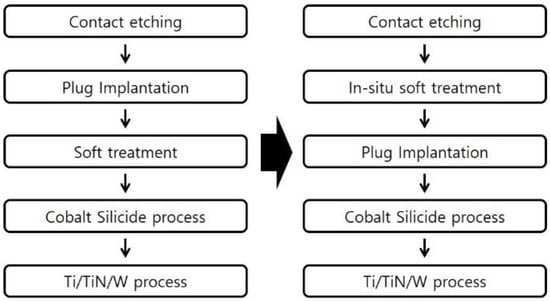
Figure 1.
Experimental sequences of the conventional (left) and modified (right) processes.
C4F6, C4F8, CH2F2, and CHF3 were used to remove the oxide and nitride mask layers for the contact etching. For the soft treatment, however, only hydrofluorocarbon plasma was used to remove byproducts and plasma-induced damaged silicon layers at the contacts in a short time [8]. Compared to the main contact etching process, the proportion of carbon and fluorine was reduced in order to prevent the remaining oxide mask from widening.
In general, the physical damage caused by plasma etching is induced by high energy ion bombardment on the Si. Thus, the damage is stronger as it goes to the Si surface, and a heavily damaged amorphous layer is formed from the surface [8]. There is a weakly damaged interlayer, next to the heavily damaged amorphous layer, just above the Si substrate of pure lattice condition. Because byproducts (C-N polymers) are generated on the top of the silicon surface, the polymers must first be removed using hydrogen, and then the damaged silicon layer must be removed with fluorine. Most importantly, the applied time was precisely controlled from 0 s to 20 s because the RC can be greatly affected by silicon loss at the contacts if the application time is too long. Because the plasma-damaged amorphous layer is thickly formed at the bottom of the contact and becomes relatively thinner as it goes toward the top of the sidewall, the critical dimension (CD) of the top of the contact gradually widens as the etching time exceeds 20 s. Moreover, hot electron–induced punchthrough (HEIP) degradation begins to deteriorate seriously when applying the treatment for more than 20 s. After plug implantation, cobalt and tungsten processes with a titanium/titanium nitride layer were employed.
Transmission electron microscope (TEM) analysis was performed to confirm how much the damaged layer was reduced by the added soft treatment process and the shape of the contact. TEM images of the silicon surface of the fabricated DC contacts are shown in Figure 2. In the case of Figure 2a, only the standard contact etching was performed without the in situ soft treatment, whereas the treatment was performed in the cases of Figure 2b,c for 10 s and 20 s, respectively. In the case of Figure 2d, a 30% reduced power was applied to originally reduce the damage by the plasma etching power itself. In the case of Figure 2a, the thickness of the remaining amorphous layer at the contact bottom was 52 Å, and in the cases of Figure 2b,c, the damaged layer thickness was reduced to 42 Å and 35 Å, respectively. It was confirmed that the damaged layer was reduced by 19% by applying the treatment for only 10 s and by 33% when applying the treatment for 20 s. On the other hand, the damaged layer is the thinnest in the case of Figure 2d, which is only 17 Å. However, the shapes of the contacts, especially the silicon substrate recesses, show many changes. Because the RF power itself was reduced by 30%, the plasma-damaged layer decreased, but it is easily found that the silicon recess in the depth direction also decreased. As shown in Figure 2a–c, the values of the silicon recess were similar to 130 or 131 Å when 0 s, 10 s, and 20 s were applied, but it was reduced to 110 Å in the case of Figure 2d. Even if the soft treatment process was performed for up to 20 s, only the thickness of the damaged layer was reduced without affecting the silicon recess. However, when the power was reduced by 30%, the silicon recess filled with W and TiN decreased by 20 Å, resulting in a large change in the shape of the contact. Since the DCs of DRAM devices have various sizes and depths, the changes in physical dimensions, as in the case of Figure 2d, may cause serious process failures. For example, the contact between word lines and bit lines, which is one of the thinnest and the longest contacts, was highly likely to be unetched in the case of Figure 2d.
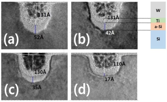
Figure 2.
TEM images of the Si contacts with application of the soft treatment process for (a) 0 s, (b) 10 s, and (c) 20 s. (d) is for 30% reduced etching power.
Different sizes of the contact chain structures fabricated in the test element group (TEG) were used to define the RC characteristics. The electrical tests, including RC, I-V, and HEIP, were conducted using an Agilent HP4072 system [9].
3. Results and Discussion
The measured RC values of (a) n+ contacts (for the source and the drain of NMOSFETs) and (b) p+ contacts (for the source and the drain of PMOSFETs) at a hot temperature (85 °C) are shown in Figure 3. As the soft treatment time increases, the resistances of all n+/p+ contacts decreased for all sizes. It is shown in Figure 3a that the n+ RC was reduced from 2.0% to 5.7% and from 5.2% to 14.1% when the in situ soft treatment was applied for 10 s and 20 s, respectively. Additionally, in the case of the p+ contact (Figure 3b), the RC was reduced from 4.5% to 8.9% with 10 s of the soft treatment and from 13.0% to 16.4% with 20 s of the soft treatment. The RC values of 0 s in Figure 3 correspond to the contact resistances of the conventional scheme. In the conventional scheme, there is no process for removing the damaged layer before the plug implantation process. Based on the layout contact size of 8460 nm2, the p+ RC decreased by 8.9% from 10765 Ω to 9805 Ω, and n+ RC decreased by 5.7% from 924 Ω to 871 Ω. This shows that the effect of improving the resistance in the p+ contacts is more pronounced than in the n+ contacts due to the reduced dopant blocking effects of the subsequent plug implantation process. To improve RC, it is important to remove the plasma-damaged layer itself, but the order of the removal process is also important. In other words, it is key to remove the amorphous layer before the subsequent plug ion implantation process is applied, and the reduced damaged layer facilitates penetration of the ions. In this experiment, arsenic ions were injected into the N+ contact and boron ions were injected at a high concentration into the p+ contact in order to make the contacts more ohmic. Because the boron ion is lighter than the arsenic ion, the effect of removing the damaged layer is more significant.
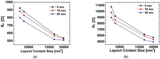
Figure 3.
The contact resistances as a function of the sizes and the processing time. (a) N+ contacts and (b) P+ contacts.
At a cold temperature (−25 °C), this RC reduction effect is more convincing. Generally, RC increases exponentially with decreasing temperature and with increasing barrier height [10]. This increase in resistances at a cold temperature is one of the biggest difficulties in automotive applications that must ensure operation over a wide temperature range. For this reason, this experiment focuses on improving the cold characteristics through decreasing the RC. As shown in the black solid and dashed lines of Figure 4, the RC at a cold temperature was increased in terms of both the median and the dispersion. The median value was largely increased by 31.9% from 6067 Ω to 8003 Ω, and the standard deviation was also increased by 43.4% from 157 Ω to 225 Ω. Both the median and the dispersion of the RC increased when the soft treatment was applied for 10 s as well, as shown in the red solid and dashed lines. However, the percentages of those increments were reduced to 27.6% for the median and 33.3% for the standard deviation. The standard deviation at −25 °C decreased from 225 Ω to 124 Ω after applying the soft treatment process for 10 s. This value is even less than 157 Ω, which is the standard deviation at a hot temperature when the soft treatment technique is not applied.
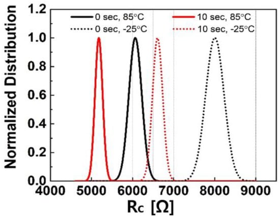
Figure 4.
Normalized median and distributions plot of the contact resistances with different temperatures and the processing time.
These results, in which a short time process can reduce both the dispersion and median values of the P + contact resistance by large amounts, show the possibilities of DRAM devices in cold temperature applications. It is found that the increase in RC at a cold temperature is greatly improved by applying the treatment process for only 10 s. The median value is a key factor that can enhance the performance of the single MOSFETs and reduce the delay time of the inverter chains. Additionally, the dispersion reduction effect can lead to more stable and predictable operation of the devices, resulting in fewer failures in terms of yields, which must satisfy conditions in a wide range of temperatures.
To confirm the effect of reducing the RC in a single PMOSFET, the electrical properties of the device fabricated in TEG were analyzed. Figure 5a shows the saturation current (IDSAT) plot measured at 85 °C as a function of the threshold voltage (VTH). We found that the IDSAT increased by 4% at the same VTH when the soft treatment was applied for 15 s. In general, cold temperature characteristics of PMOSFETs are not good compared to NMOSFETs, due to their inherent issues. In the group with a 15 s application, the cold current characteristics were improved by about 3% when compared to the group with no application, as shown in Figure 5b. In the normal group, indicated by black squares, it seems that the saturation current at −25 °C is about 96% of the saturation current at 85 °C, which is less than the 1:1 line. In the 15 s application group, indicated by red circles, however, the performance was enhanced to 98.5%. It can be seen that the increase in VTH and the decrease in IDSAT caused by the cold temperature operations can be overcome by reducing the contact resistances using the simple in situ soft treatment technique.
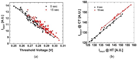
Figure 5.
Single PMOSFET characteristics. (a) IDSAT as a function of processing time and threshold voltages. (b) IDSAT relationship between hot (85 ℃) and cold (−25 ℃) temperature.
Figure 6 shows the normal distributions of the propagation delay times (tPD) with different temperatures (85 °C and −25 °C) and operating voltages (0.95 V and 1.2 V). The tPD is measured from the inverter chains which are composed of 100 inverters. By applying a simple electrical inverter model, the tPD can be written as follows:
where CL is a loading cap and REFF,N and REFF,P are the effective resistances of the NMOSFETs and the PMOSFETs, respectively. CL is an AC parameter, including overlap cap (COV), junction cap (CJ), oxide cap (COX), and line cap (CLINE). REFF is a DC parameter, including the external resistance (REXT), the source/drain resistance (RSD), and the channel resistance (RCH). Except for the REXT, the CL is mostly determined at the design stage because it is strongly affected by layout structures. RCH and RSD are important parameters to realize a low VTH transistor scheme. Among these parameters, CJ, REXT, and VTH are dominantly affected by temperature. At a cold temperature, in general, IDSAT is rather reduced in PMOSFETs, since the rapid increase in RC dominates the increase in the mobility by reduced lattice scattering. Therefore, the dramatic decrease in RC by the application of soft treatment for 10 s has a great effect on the tPD, especially in low-temperature and low-voltage operation.
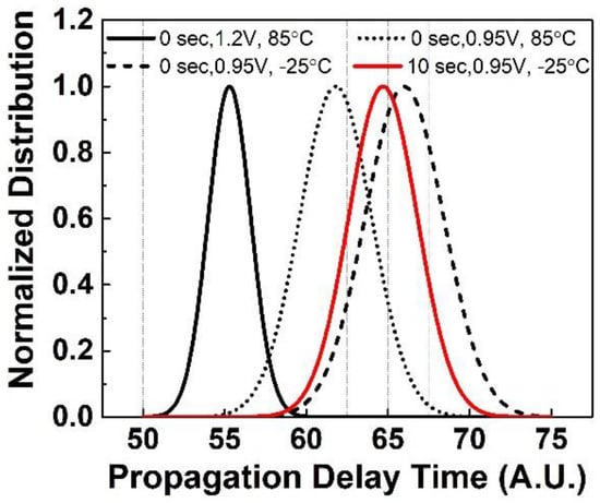
Figure 6.
Normalized median and distributions plot of the propagation delay time with different temperatures, voltages, and processing times.
As seen by comparing the black solid line with the small dashed line, the median value of the tPD increased by 11.7% from 55.3 to 61.8 as the operating voltage decreased from 1.2 V to 0.95 V. The standard deviation also increased from 1.3 to 2.2. This speed limit makes the mobile applications of DRAM more difficult. In addition, if cold-temperature operating conditions are added to this, both the median value and the 1-sigma value increase similarly to the large black dashed line. In this case, the median value of the tPD increases by 19.3% from 55.3 to 66 and the standard deviation increases by 84.6% from 1.3 to 2.4. The difference of the tPD between 85 °C and −25 °C was 4.2 when the soft treatment was not applied. It was reduced to 2.9 when applying treatment for 10 s as shown by the red solid line in Figure 6. If it is necessary to guarantee a DRAM operation speed limit up to 70 or less to commercialize a product, a significant portion of the chips in a wafer will be rejected in the group that does not apply the soft treatment, resulting in a yield drop by cold temperature tests. However, it is possible to reduce the overall distributions of the tPD by only carrying out the process for 10 s, thereby saving a large number of chips. In other words, an increase in the tPD due to degraded PMOSFET characteristics at cold temperatures can be improved to ensure a more stable and precise operating speed.
Temperature-related parameters of the propagation delay times are defined as VTH and REXT, and Figure 7 shows the tPD characteristics as a function of them. Here, the tPD skew shows the difference between the cold-temperature and hot-temperature values. As expressed in the formula of the simple inverter electrical model in Equation (1), for the group in which VTH is low, within 20% of the entire samples have mostly negative tPD skew values (see the black squares). On the other hand, for the group in which VTH is high, over 70% of the entire samples (see the blue triangles) are mostly located in the positive region. Regardless of the high and low groups of VTH, the tPD skew decreases when the contact resistance decreases in all groups. According to our experiments, the tPD skew decreases by 0.5 ps when the RC decreases by 1100 Ω. The reduction in this tPD skew shows that it can lead to more stable and predictable results than other conventional automotive applications used in a wide range of temperatures.
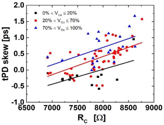
Figure 7.
tPD median skew between hot (85 °C) and cold (−25 °C) temperatures as a function of threshold voltages and contact resistances.
As the distance between the DC and the gate becomes smaller and smaller, it is considered essential to check the immunity to hot electron–induced punchthrough (HEIP) reliability. This is even more important in DRAM operations, since there are PMOSFETs operating at a high voltage (VPP) as a part of the sub word line driver (SWD) [11]. For this, we applied an AC stress to the PMOSFET with the conditions VG = VB = VPP, VD = –0.3 V, and an AC pulse from 0 to VPP was forced on VS. To accelerate the tests, the time was fixed to 50 s and the VPP was strengthened to 4–6 V. All the tests were conducted at room temperature, which is known to be the worst condition for electron trapping [11].
The results of the IOFF measurement in log scale are shown in Figure 8. As VSTRESS increases, IOFF increases rapidly at a certain voltage in each group. In the soft treatment application group indicated by red circles, the graph shifts to the left. This is because the gate-induced drain leakage (GIDL) and the plug effect deteriorate as the subsequent plug implantation is strengthened with the reduction in the plasma-induced-damaged layer. For reference, the graph is shifted further to the left when the amount of RC reduction is adjusted by strengthening the plug implantation by 25%. By defining VHEIP as VSTRESS when IOFF increased by 100 nA, it is found that 10 to 15 s is an appropriate process time as shown in the inset of Figure 8. VHEIP decreased by increasing the soft treatment time, but the degradation did not appear until after 10 s of treatment. VHEIP was reduced by more than 100 mV for 20 s, so that the electric field of the channel edge was seriously affected. Therefore, treatment up to 10 s has the effect of reducing resistance and reducing the tPD and is less sensitive to HEIP reliability issues; thus, it is much more efficient than other resistance reduction techniques, such as strengthening the plug implantation.
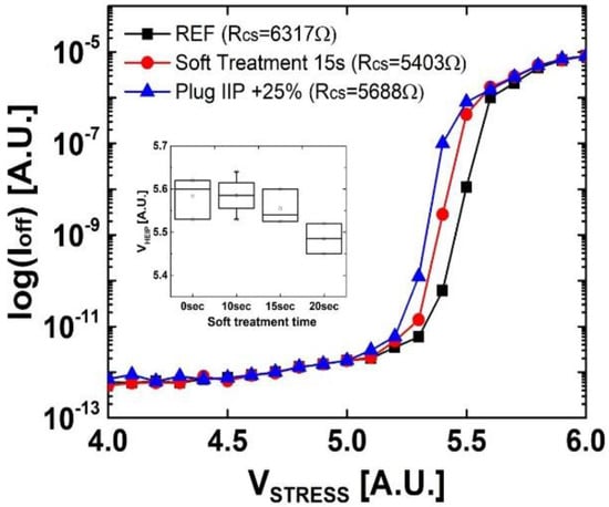
Figure 8.
I-V curves for HEIP reliability. VHEIP as a function of processing time (inset).
4. Conclusions
Our results show that the median values and dispersion of contact resistances can be greatly reduced by removing the plasma-damaged silicon layer of the source/drain contacts. Here, an in situ soft treatment process for 10 to 15 s was used as a method of lowering the RC, and contact resistances of all sizes were reduced. As a result, the saturation current of the PMOSFETs increased by 4% at the cold temperature, and the propagation delay time of the inverter chain circuits was also reduced at low operating voltage and temperature. Since this soft treatment process is performed in situ with the contact etch process, there are no additional steps, and it has a great advantage in terms of cost because the process time is short. In addition, unlike with ion implantation solutions, it is possible to reduce the resistances of both the n+ and p+ contacts with a single process, and it can be easily applied because the immunity to HEIP reliability is small. Finally, the method does not change the critical dimensions or depths of the contacts. If the process time is applied excessively, however, the pure silicon can be lost, resulting in increased resistances and deteriorated plug effect or reliability. Therefore, the etching power and the interface of the contacts must be analyzed in advance.
Author Contributions
Conceptualization, J.S.; methodology, E.L., S.H.; software, J.S.; validation, J.K., J.O. and B.C.; structure analysis, J.S.; investigation, E.L., S.H.; writing—original draft preparation, J.S.; writing—review and editing, E.L., S.H., J.K., J.O. and B.C. All authors have read and agreed to the published version of the manuscript.
Funding
This research was funded and conducted under the Competency Development Program for Industry Specialists of the Korean Ministry of Trade, Industry and Energy (MOTIE), operated by Korean Institute for Advancement of Technology (KIAT).
Institutional Review Board Statement
Not applicable.
Informed Consent Statement
Not applicable.
Data Availability Statement
Not applicable.
Conflicts of Interest
The authors declare no conflict of interest.
References
- Yeo, Y.C. Advanced source/drain engineering for MOSFETs: Schottky barrier height tuning for contact resistance reduction. ECS Trans. 2010, 28, 91. [Google Scholar] [CrossRef]
- Lee, J.H.; Yeo, I.S.; Lee, J.Y.; Lee, S.K. Analysis of the improved contact resistance in metal-p+ silicon Schottky barriers using the BF 2/B mixed implantation. Appl. Phys. Lett. 1999, 75, 1284–1286. [Google Scholar] [CrossRef]
- Menghini, M.A.; Homm, P.; Su, C.Y.; Kittl, J.A.; Tomita, R.; Hegde, G.; Lee, J.G.; Hyun, S.; Bowen, C.; Rodder, M.S.; et al. Modulation of the Schottky Barrier Height for CMOS advanced contacts. Microelectron. Eng. 2016, 156, 82–85. [Google Scholar] [CrossRef]
- Song, Y.; Zhou, H.; Xu, Q. Source/drain technologies for the scaling of nanoscale CMOS device. Solid State Sci. 2011, 13, 294–305. [Google Scholar] [CrossRef]
- Lee, S.H.; Park, S.G.; Kim, S.D.; Jung, H.C.; Kim, I.G.; Kang, D.H.; Park, J.H. Suppression of boron diffusion using carbon co-implantation in DRAM. Mater. Res. Bull. 2016, 82, 22–25. [Google Scholar] [CrossRef]
- Khaja, F.A.; Colombeau, B.; Thanigaivelan, T.; Ramappa, D.; Henry, T. Physical understanding of cryogenic implant benefits for electrical junction stability. Appl. Phys. Lett. 2012, 100, 112102. [Google Scholar] [CrossRef]
- Koyanagi, M.; Lewis, A.G.; Martin, R.A.; Huang, T.Y.; Chen, J.Y. Hot-electron-induced punchthrough (HEIP) effect in submicrometer PMOSFET’s. IEEE Trans. Electron Devices 1987, 34, 839–844. [Google Scholar] [CrossRef]
- Yoon, J.; Lee, J.; Yoo, W.J. Removal of Plasma-Induced Physical Damage Formed in Nanoscale Three-Dimensional FinFETs. Nano 2017, 12, 1750099. [Google Scholar] [CrossRef]
- Agilent Technologies. Agilent Technologies 4070 Series Semiconductor Parametric Tester User’s Guide; Agilent Technologies: Santa Clara, CA, USA, 2000. [Google Scholar]
- Chang, C.-Y.; Fang, Y.K.; Sze, S.M. Specific contact resistance of metal-semiconductor barriers. Solid-State Electron. 1971, 14, 541–550. [Google Scholar] [CrossRef]
- Park, S.; Jung, H.; Oh, J.; Kim, I.; Hong, H.; Jin, G.; Roh, Y. Off-state degradation with ac bias in PMOSFET. Microelectron. Reliab. 2016, 65, 16–19. [Google Scholar] [CrossRef]
Publisher’s Note: MDPI stays neutral with regard to jurisdictional claims in published maps and institutional affiliations. |
© 2022 by the authors. Licensee MDPI, Basel, Switzerland. This article is an open access article distributed under the terms and conditions of the Creative Commons Attribution (CC BY) license (https://creativecommons.org/licenses/by/4.0/).