Article

A Miniaturized Closed-Loop Optogenetic Brain Stimulation Device

by
Lekshmy Sudha Kumari
* and
Abbas Z. Kouzani
School of Engineering, Deakin University, Geelong, VIC 3216, Australia
*
Author to whom correspondence should be addressed.
Electronics 2022, 11(10), 1591; https://doi.org/10.3390/electronics11101591
Submission received: 26 March 2022 / Revised: 13 May 2022 / Accepted: 15 May 2022 / Published: 17 May 2022
(This article belongs to the Section Bioelectronics)

Abstract

:
This paper presents a tetherless and miniaturized closed-loop optogenetic brain stimulation device, designed as a back mountable device for laboratory mice. The device has the ability to sense the biomarkers corresponding to major depressive disorder (MDD) from local field potential (LFP), and produces a feedback signal to control the closed-loop operation after on-device processing of the sensed signals. MDD is a chronic neurological disorder and there are still many unanswered questions about the underlying neurological mechanisms behind its occurrence. Along with other brain stimulation paradigms, optogenetics has recently proved effective in the study of MDD. Most of these experiments have used tethered and connected devices. However, the use of tethered devices in optogenetic brain stimulation experiments has the drawback of hindering the free movement of the laboratory animal subjects undergoing stimulation. To address this issue, the proposed device is small, light-weight, untethered, and back-mountable. The device consists of: (i) an optrode which houses an electrode for collecting neural signals, an optical source for delivering light stimulations, and a temperature sensor for monitoring the temperature increase at the stimulation site, (ii) a neural sensor for acquisition and pre-processing of the neural signals to obtain LFP signals in the frequency range of 4 to 200 Hz, as electrophysiological biomarkers of MDD (iii) a classifier for classification of the signal into four classes: normal, abnormal alpha, abnormal theta, and abnormal gamma oscillations, (iv) a control algorithm to select stimulation parameters based on the input class, and (v) a stimulator for generating light stimulations. The design, implementation, and evaluation of the device are presented, and the results are discussed. The neural sensor and the stimulator are circular in shape with a radius of 8 mm. Pre-recorded neural signals from the mouse hippocampus are used for the evaluation of the device.

1. Introduction

Identification of the roles of specific neuronal circuits in different brain functions, and understanding their roles in causing neurological disorders, are important topics of investigation. In the recent years, different brain stimulation techniques, both invasive and non-invasive, have been used in the research and treatment of various neurological diseases. Non-invasive brain stimulation techniques include transcranial magnetic stimulation (TMS) [1], transcranial electrical stimulation (tES) [2], transcranial direct current stimulation (tDCS) [3], transcranial alternating current stimulation (tACS) [4] etc. Invasive brain stimulation techniques include electrical deep brain stimulation (DBS) and optogenetic brain stimulation (OBS). While electrical DBS is currently being used for the treatment of various neurological disorders, it has the shortcoming of not being able to stimulate a specific neuronal circuit [5]. Optogenetics uses light to control neurons with high spatial and temporal resolution. Optogenetic brain stimulation (OBS) is capable of modulating the activity of specific neuronal populations, and can improve the effectiveness of brain stimulation paradigms. In optogenetics, light-sensitive proteins called opsins are genetically encoded into the neurons, and the neuronal activity is modulated by delivering light [6]. Recently, optogenetics has been intensively studied in animal disease models for identifying the role of specific neuronal populations in various neurological conditions including Parkinson’s disease (PD) [7], major depressive disorder (MDD), epilepsy [8], Alzheimer’s disease (AD) [9], among others.
On the device engineering side, most of the current commercial optogenetic systems use an open-loop control [10] in which the stimulation parameters are manually modified [11]. Closed-loop neurostimulation is a form of neurostimulation that provides therapeutic stimulation only when necessary [12], thus it is referred to as a ‘brain-dependent brain stimulation’ and is understood to have better performance than its open-loop counterpart [13]. Studies of closed-loop electrical DBS in the management of various neurological conditions have shown favorable results by offering the ability to achieve better control of patient symptoms and side effects than conventional open-loop DBS [14]. Closed-loop OBS (clOBS) has also been explored for conditions like PD, epilepsy [15], etc., in small laboratory animal models of these diseases. To fully leverage clOBS, it is important that the clOBS devices are optimized in terms of size, portability, power, and functionality to fit the size of the small laboratory animal subjects, and to ensure efficient use with freely behaving animal models of diseases.
Considering the literature on clOBS devices, earlier versions of clOBS were large, untethered systems. For example in [16], epileptic seizures were detected in real-time from EEG of the epileptic animal subject, through digital processing of the signal using a MATLAB-based detection algorithm running on a computer. On detecting seizures, stimulation software was used to activate a laser diode to produce the stimulation light. Similar implementation of closed-loop stimulation on large benchtop devices was also presented in [17]. Miniaturization of the sensing and stimulation devices was implemented and reported by Nguyen et al. [18], where an amplifier chipwas used for the pre-processing of the raw neural input signals through 32 low-noise channels. The optical stimulations were produced using LEDs instead of laser diodes. Even when miniaturization was applied to the sensor and stimulation hardware, the sensed signals are processed on a computer to identify the biomarkers. Further miniaturization of a clOBS device was reported by Edward et al. [19], where a fully portable and head-mountable device suitable for small laboratory animals was presented. The system detected the action potentials from the raw neural signals, turning the stimulation ON when the detected signals are below a set threshold voltage. The stimulation is turned OFF when the detected signals are above the set threshold voltage. This implementation used a low-power microcontroller as the platform for running the signal processing, generation and control of stimulation pulses.
Field-programmable gate array (FPGA)-based controllers have been used to run signal processing algorithms, including artificial intelligence (AI)-based algorithms, in recent clOBS devices [20]. FPGAs have higher computational capabilities than microcontrollers, but are power-hungry. This was a drawback for untethered and portable clOBS devices. With the advent of on-device AI using small, low-power, resource-constrained microcontrollers, small AI-based signal processing has become feasible for implementation on such microcontrollers [21,22], making possible complex data analytics on microcontroller-based clOBS devices.

1.1. Motivation

Major depressive disorder (MDD) or clinical depression is a common neurological disorder, and one of the main causes of disability worldwide [23,24]. Various research groups, including Prévot et al. [21] and Wand et al. [22] have worked to identify the underlying conditions behind the occurrence of MDD. Brain-stimulation strategies have been widely used in the study of MDD [25,26]. Optogenetics is a valuable tool in this research, due to its highly specific ability to control neuronal populations [27]. Numerous studies have used optogenetics to explore the neural mechanisms involved in depression and depression-like symptoms [28,29]. For optogenetic studies conducted on laboratory animal models of MDD, miniaturization and portability are highly recommended criteria for the OBS devices.
This paper presents a miniaturized, light-weight, untethered, and back-mountable solution that hosts all the necessary components to deliver clOBS to laboratory animal subjects. The design, development, and validation of the clOBS device is presented. The paper also provides information and insights into the in vivo operation of the clOBS device.

2. Overview of the Closed-Loop Optogenetic Stimulation Device

The proposed system, as shown in Figure 1, comprises both hardware and software components. The hardware component consists of an optrode, a neural sensor, and an optogenetic stimulator. The software component consists of data acquisition, data processing (classification and the control algorithm), and output signal producing units. The optrode houses the electrode for detecting the raw neural signals, the stimulation light source, and a negative thermal coefficient (NTC) thermistor for monitoring temperature. The neural sensor senses and pre-processes the neural signals. It includes a pre-amplification stage, band-pass filter stage, and post-amplification stage. The neural sensor provides an amplification of 20,000 v/v to the very small amplitude input neural signals, after filtering out the signals not within 4 Hz to 200 Hz. 4 Hz to 200 Hz correspond to the signals in the local field potential (LFP) range which include the electrophysiological biomarkers of MDD. After the initial processing of the signal in the neural sensor, further processing is performed on the device microcontroller. The microcontroller runs a quantized deep neural network (DNN) algorithm, which classifies the digitized neural sensor output into 4 classes: normal signal, abnormal alpha signals, abnormal theta signals, and abnormal gamma signals. It is understood from the literature that abnormality in alpha (8–13 Hz), theta (4–7 Hz)), and gamma (30–200 Hz) band oscillations can be considered as a biomarker of MDD [30]. Once an abnormal class is identified, a trigger signal is sent the control algorithm to set the stimulation parameters. Based on the set stimulation parameters, stimulation pulses are generated by the optogenetic stimulator, using a LED driver. The light is delivered to the target brain region using the µLED on the optrode. Another important feature of the device is its temperature monitoring mechanism. This is done by using an NTC placed on the optrode and the related circuitry, using the microcontroller on the optogenetic stimulator. This ensures that the temperature increase caused by the stimulating light in the tissue surrounding the probe should be below the 2 °C threshold, as suggested by Peixoto et al. [31]. To prevent damage to the brain cells, the stimulation is turned off when the temperature increases above the set threshold.

3. Component Design

This section describes various components of the proposed clOBS device, including the optrode, the neural sensor, the optogenetic stimulator, the classification algorithm, the control algorithm, and the temperature monitoring algorithm.

3.1. Optrode

Optrodes are electrodes used in optogenetic devices simultaneously to record electrical activity from the target brain region, and deliver light stimulations to the brain region [32]. This subsection presents the optrode design for the proposed clOBS device, with the capability of recording electrophysiological signals, delivering optical stimulation, and performing temperature sensing. The electrophysiological signals are sensed using the sensing electrodes and the reference electrodes placed at the tip of the optrode, on either side (Figure 2). Stimulation light is delivered using a µLED placed on the optrode, and the temperature sensing realized using a negative temperature coefficient (NTC) thermistor. The optrode has been designed and fabricated for use in the closed-loop optogenetic brain stimulation device. A printed circuit board (PCB) diagram of the two sides of the probe is shown in Figure 2. It describes the connections and locations of different components in the fabricated probe. The dimension of the probe shaft is set as 4.5 mm × 0.8 mm. This dimension was chosen to match the thickness of brain cortical layers of a laboratory mouse [33]. The pointed edge guarantees the sharpness of the shaft, which could reduce potential tissue damage during implantation. The entire probe is fabricated on a two-sided flexible PCB. There are six I/O pads, three on each side, implemented on the probe to convey the input/output signals to and from the components in the probe to the external circuitry. The probe includes three functionalities: temperature sensing, electrophysiological biomarkers sensing, and light delivery.

3.1.1. Light Source

A single-channel light delivery and reading mechanism is employed, with one stimulation site for the placement of µLED. In order to activate the ChR2 transfected neurons, 470 nm light of 1 mW/mm2 irradiance is required [34]. After detailed review of optical and electrical features of various LEDs, Cree chip 2432 µLED was selected. Cree chips are capable of delivering peak optical power output of about 33 mW, suitable for closed-loop OBS. Commercially available CREE 2432 µLED was a suitable choice. Combining InGaN material and Silicon-carbide substrate, with a size of 240 µm × 320 µm, the chip is situated on the probe just above the tip.

3.1.2. Sensing and Reference Electrodes

Neural activity is sensed by two sensing electrodes of triangular shape with 100 µm sides. The electrodes were placed adjacent to the µLED, along the tip of the probe on both sides. One of the electrodes acts as the reference electrode, while the other acts as the channel input to the neural sensing circuit.

3.1.3. Temperature Sensor
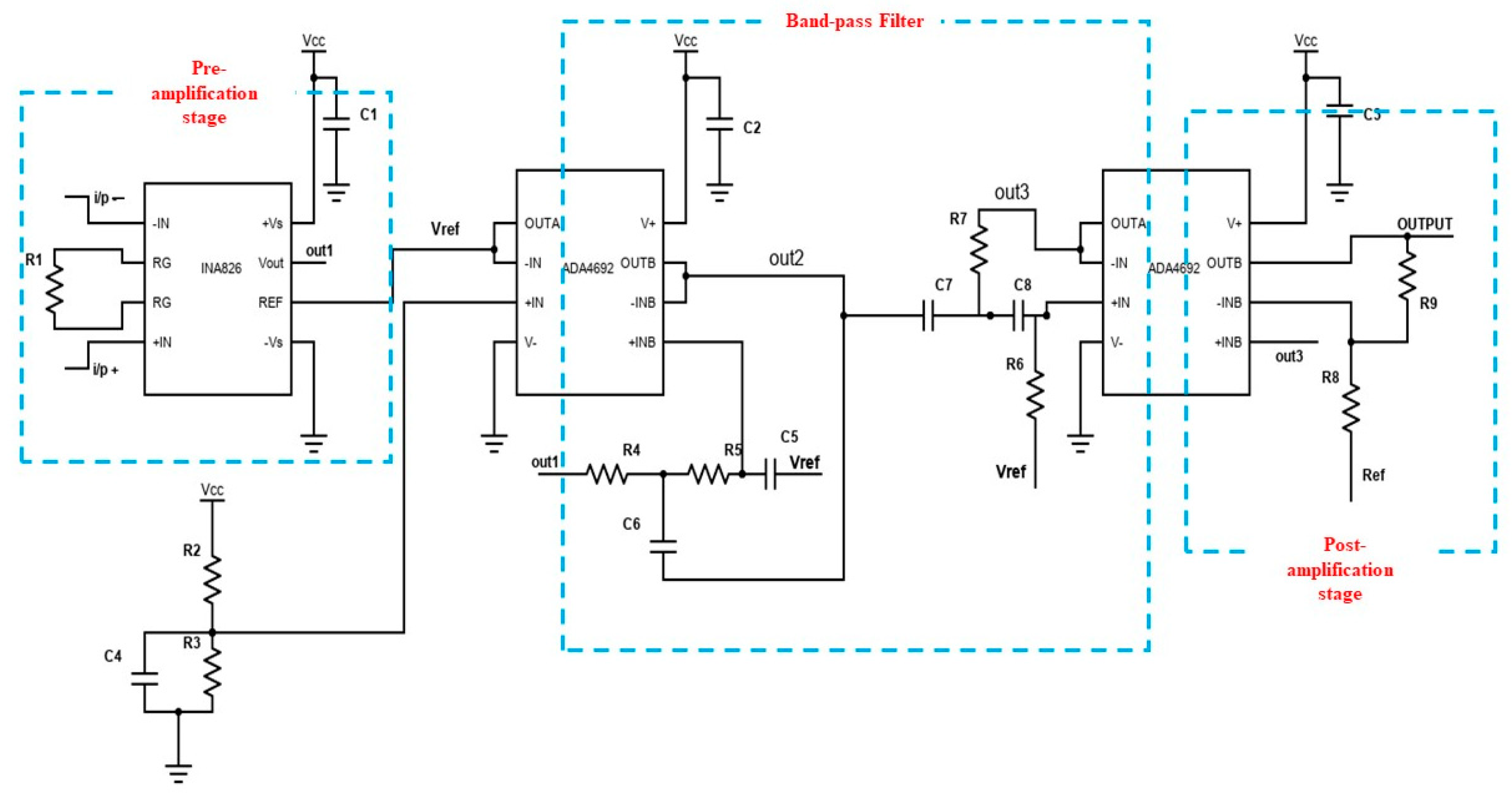
In order to sense the temperature near the area of illumination, an NTC is used. NTC thermistors have the advantage of fast response time over narrow temperature range, no contact and lead resistance problems due to large resistance, good sensitivity, low cost, and are the most commonly used thermistors in medical devices. A commercially available ERTJZET202J by Panasonic was selected for the design. It has a size of 0.6 mm × 0.3 mm which is compatible with the size of the µLED. The NTC chip is situated on the back of the probe, behind the µLED.
The top and bottom images of the fabricated probe are shown in Figure 2. The top section contains three I/O pads, pads for attaching the µLED and a triangular sensing electrode at the tip. The bottom contains three I/O pads, pads for attaching the NTC thermistor and a triangular reference electrode at the tip.

3.2. Neural Sensor

The neural sensor circuit, called the TinyLFP, was presented in the authors’ earlier work [35]. The circuit diagram is summarized in Figure 3. TinyLFP includes the circuits required to perform the acquisition and initial processing of the neural signals. It is a single-channel device that performs the amplification and filtering of low-amplitude LFP signals from the sensed raw neural signals. This is completed using (i) an ultra-low power single channel precision instrumentation amplifier INA826 (3 mm × 3 mm) from Texas Instruments, and (ii) a low-power dual Opamp ADA4692 (2 mm × 2 mm) from Analog Devices, as well as other passive components.

3.2.1. Pre-Amplification

The low-noise, high-gain instrumentation amplifier INA826 forms the pre-amplification stage. It takes the input from the sensing and reference electrodes, and gives a differential amplification of 100 v/v. The gain of 100 v/v is achieved by using a resistor R1 of 499 Ω, from the gain equation of INA826 given by:
G ain = 1 + 49.4   k R

3.2.2. Filtering

Following the initial stage of amplification, the pre-amplified signals undergo band-pass filtering. This is done to filter out unwanted frequencies from the raw neural signals. The band-pass filter has a lower cut-off frequency of 4 Hz and an upper cut-off frequency of 200 Hz, to obtain LFP signals in the theta, alpha, beta, and gamma bands. This is realized using an ADA4692 dual opamp chip. The upper and lower cut-off frequencies are set by using R4 = R5 = 205 kΩ, R6 = R7 = 84.5 kΩ, C5 = C6 = 3.9 nF, and C7 = C8 = 0.47 µF from the cut-off frequency equation given as:
Cut off   frequency = 1 2 π R C

3.2.3. Post-Amplification

The pre-amplified and filtered signal is amplified further using the post-amplification stage, which is realized using another opamp circuit in ADA4692. The post-amplifier gives an amplification of 200 v/v to the filtered LFP signals. A 200 v/v amplification is set using R8 = 200 Ω and R9 = 40.2 kΩ, from the amplifier gain equation given by:
  G a i n = 1 + R f e e d b a c k R
This helps to achieve an overall amplification of 20,000 v/v for the LFP signals in the range 2 Hz to 200 Hz from the raw neural input signals.

3.2.4. Power Supply and Virtual Ground

The neural sensor is powered using a 3.3 V power source. To enable single supply operation of the neural sensor circuit, and to realize a single supply analog to digital converter (ADC), a virtual ground is maintained by means of a level shifter. This is done using a voltage divider circuit (R2 = R3 = 100 kΩ) followed by an opamp amplifier (ADA4692) in voltage follower configuration. With 3.3 V as the supply voltage, the ground is shifted to about 1.65 V.

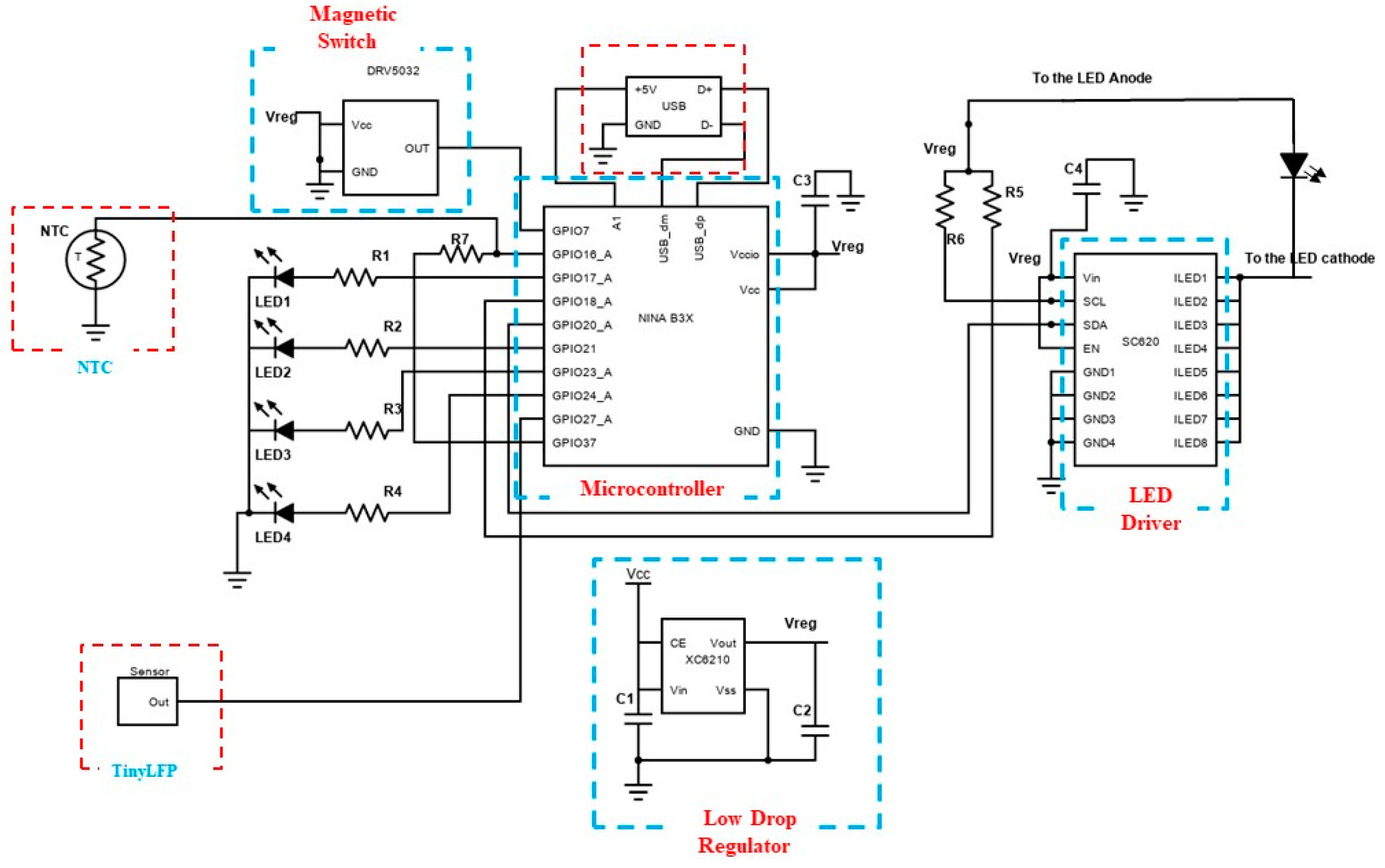
3.3. Optogenetic Stimulator

In closed-loop optogenetic systems, the stimulation circuit is used to control the operation of the light source, based on the neural signals. The pulse width, frequency, and intensity of stimulation light can be modified according to the output of the neural sensor. This is achieved by sampling and digitizing the amplified neural signal, running the classification and control algorithm, and controlling the light source based on the output of the control algorithm. The circuit diagram of the stimulator is shown in Figure 4. The stimulator circuit consists of a microcontroller, a regulator, a voltage supply, an LED driver, and a magnetic switch.

3.3.1. Microcontroller

A 32-bit ARM Cortex-M4 microcontroller, nRF52840 by Nordic Semiconductors [36] is used as the control module in the device. The microcontroller controls the stimulation output, implements system logic, and facilitates programmability. A NINA B306 stand-alone module with an nRF52840 microcontroller is used in the circuit design, ensuring the ease of microcontroller programming using an USB interface. USB programming is achieved by using the pins USB_DP, USB_DM, and the Vbus. To enable USB programming, a 5 V supply input is connected to the Vbus pin. The nRF52840 has substantial memory availability for flash memory (1 MB) and RAM (256 kB). It has 48 general purpose I/O pins, 12-bit 8 channel 200 ksps A/D converters, and a USB 2.0 12 Mbps controller. The NINA has the dimensions 11.6 mm × 10 mm × 2.23 mm, facilitating a miniaturized design including all the advanced features of the nRF52840 microcontroller. The microcontroller can run on voltages as low as 1.7 V and includes an integrated 64 MHz oscillator. A pulse width modulation (PWM) is used to control operation of the stimulation LED through an SC620 current sink LED driver.

3.3.2. Current Sink

An SC620 by Semtech [37], with eight identical, independently controlled current sinks drives the µLED on the optrode for generating the stimulation light. The LED can be driven by connecting the anode of the LED to the power supply, and the cathode to the input pin of the current sink. The current sink has an adjustable current setting register, which allows variable current setting step sizes from 31.25 µA to 500 µA. This gives a good range of options for light intensity settings. An I2C interface bus is used for programming the current control register. The I2C interface involves serial clock (SCL) and serial data (SDA) lines, which are connected to Vcc through the pull-up resistors, R5 and R6. The ultra-miniature SC620 is supplied in a 3 mm × 3 mm MLPQ-UT-16 package. It includes protection features such as short circuit current limit, thermal protection, and under-voltage lockout across all load conditions.

3.3.3. Magnetic Switch

Along with the above-described features, a physical interface has been created to enable activation and deactivation of the device, to facilitate easy user control of the board. A Hall effect sensor, DRV5032 from Texas Instruments, operates as a magnetic switch [38]. Incorporating the DRV5032, the device can be turned ON and OFF manually using a magnet. When the applied magnetic flux density exceeds the threshold, the device outputs a low voltage. The output is connected to the microcontroller GPIO pin P0.25, set at input mode. This means that researchers need only to move a magnet within the active area of the sensor and the microcontroller can enable and disable the stimulation. This sensor has a very low power consumption of 1.6 µA at 3.3 V power supply and a tiny packaging size of 1.1 mm × 1.4 mm × 0.4 mm.

3.3.4. Power Source and Regulator

The entire clOBS device is powered by a 3.7 V 30 mAh LiPo battery. The XC6210 low-dropout regulator (LDO) from Torex Semiconductor [39] is used to ensure low noise regulation of the analog supply voltages. This chip was selected because it offers low noise and high output current. The regulator takes 1.5–6 V and regulates it to a stable 3.3 V level for powering the components on the optogenetic stimulator board and the neural sensor board.

3.4. Software Components

The software component was developed using C programming language and uploaded into the nRF52840 microcontroller after installing the Arduino bootloader [40]. The pseudocode is given in Figure 5. The firmware consists of three modules: data acquisition module, data processing module, and output signal generation module.

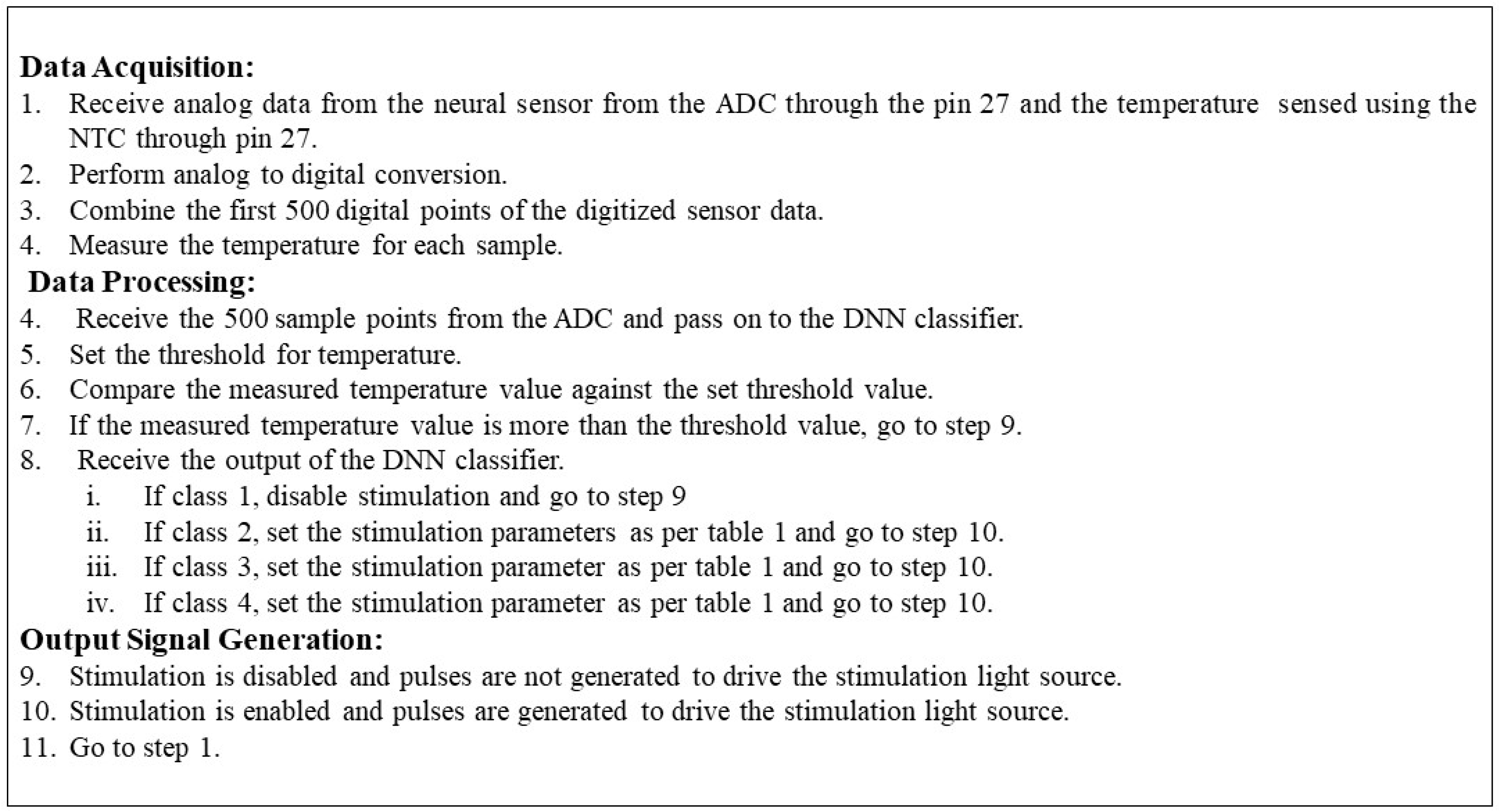
3.4.1. Data Acquisition

The data acquisition module includes code to read the pre-processed analog neural data from the neural sensor and the temperature monitoring circuit. The neural data is read using the microcontroller GPIO27_A pin. The ADC is enabled and the neural data is sampled. The neural signal is then given to a Deep Neural Network (DNN) classifier, which has been described in detail in a paper by Kumari and Kouzani [41]. The classifier takes the neural signals, with a dimension of 500 samples, and classifies them into one of four classes: normal signal (class1), abnormal theta (class2), abnormal alpha (class3), or abnormal gamma (class4). Because the input dimension of the classifier is 500, the sampled neural data is continuously stored in the flash memory and given to the DNN after 500 samples have been received. Additionally, the analog data from the NTC circuit for temperature monitoring is sensed and sampled using the ADC on pin GPIO20_A.

3.4.2. Data Processing

Data processing includes the classification and control algorithms. During data processing, the acquired neural signals are classified using a seven-layer fully connected DNN-based classifier. The DNN network is trained with four sets of training data: normal signals, signals with modified amplitude in the theta band oscillations, signals with modified amplitude in the alpha band oscillations, and signals with modified amplitude in the gamma band oscillations. These modified signals represent the biomarkers of MDD, according to the literature described in Section 1.1. Based on the classification output, an On/Off control algorithm is used either to set the stimulation parameters (the frequency, pulse width, and duty cycle of the output pulse) if the signal corresponds to class 2, class 3, or class 4. The stimulation is stopped if the classification shows a normal signal. The stimulation parameters are set as per Table 1, based on safe optogenetic stimulation parameters [42]. Along with this, temperature is measured from the sampled values using the NTC thermistor equation, after applying a calibration. This value is then used in the control the On/Off control algorithm, where the stimulation is turned off when the measured temperature goes above the set threshold value.

3.4.3. Output Signal Generation
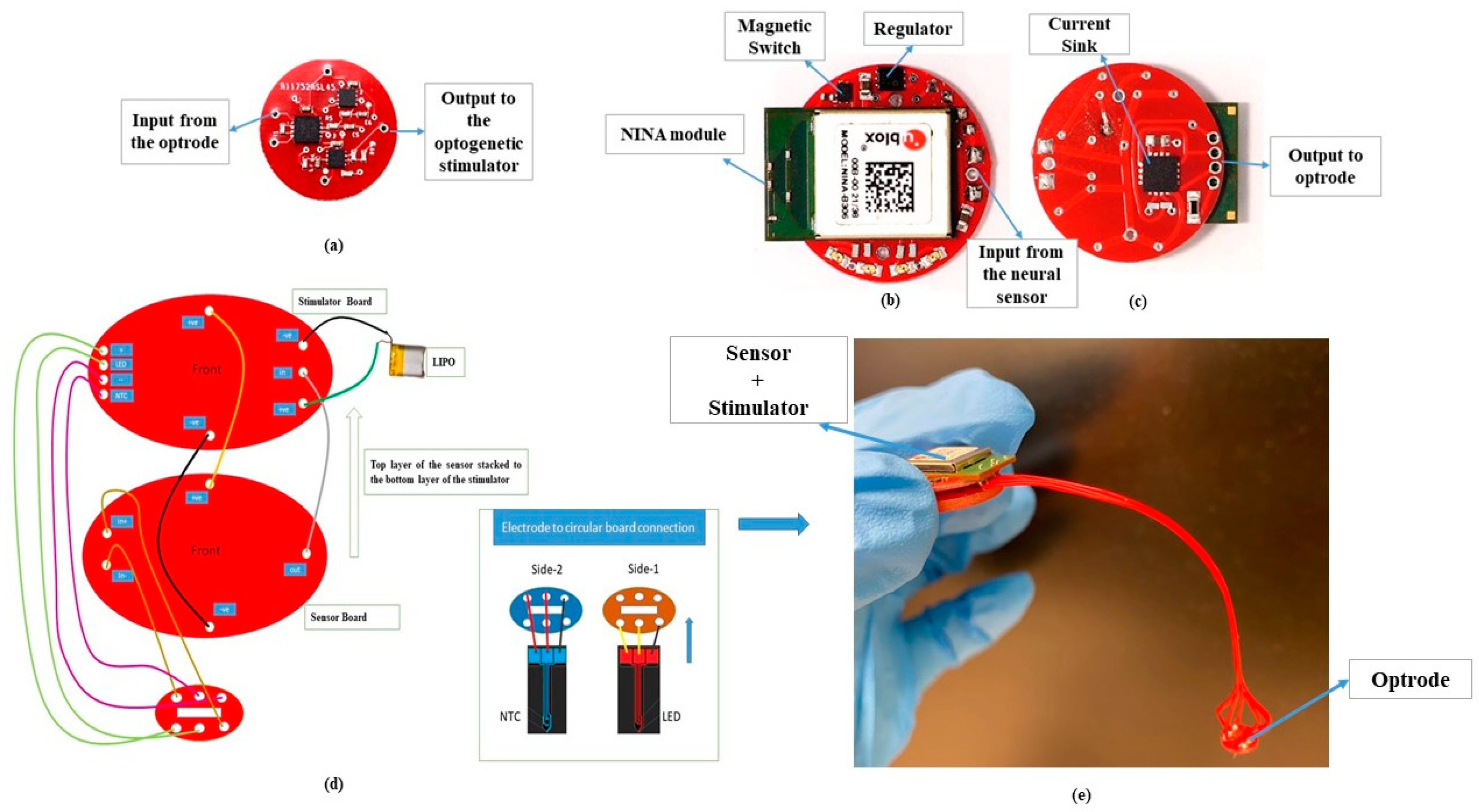
The output signal generation module generates pulses to modulate the stimulation LED. The stimulation pulses for specific parameters are set in the data processing module, and turned on if an abnormal signal is detected. The stimulation is turned off when the incoming signal falls into the normal class.

4. Physical Design

Implementation of the clOBS device was achieved by the design and fabrication of printed circuit boards (PCB). Three separate boards were designed: one for the optrode, one for the neural sensor, and one for the optogenetic stimulator. After validation of each board, the boards were stacked to form the final device, as shown in Figure 6. The device was designed to be used as a back-mountable closed-loop optogenetic stimulation device for laboratory animal subjects. The boards were fabricated in a two-layer configuration. A description of the optrode board is given in Section 3.1. Both the neural sensor and optogenetic stimulator boards were designed in a circular shape and measure 8 mm in radius. In order to connect the optrode to the stacked device, a separate printed board in a circular shape was developed. The I/O pads in the optrode were connected to the pads on the circular board for easy connection to the device. The final back-mountable device is shown in Figure 6e.

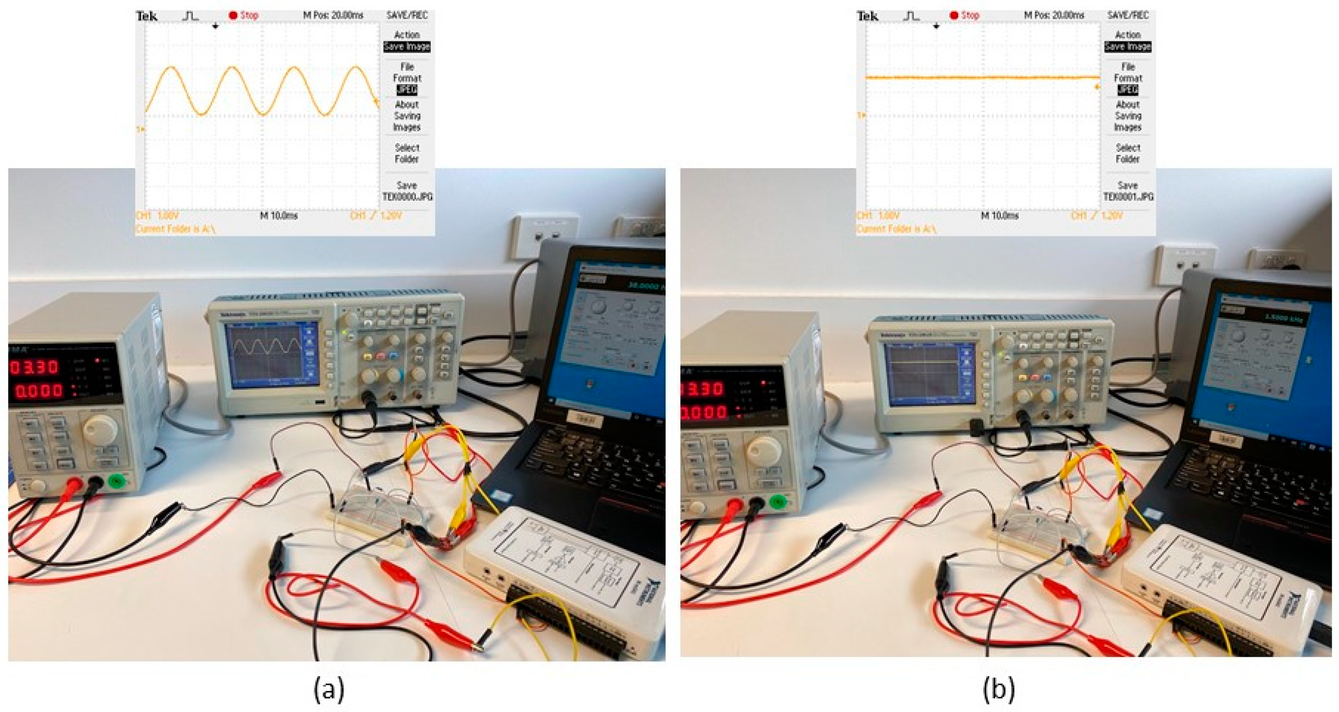
5. Experimental Design and Results

This section describes the experimental evaluation of the device, and the results obtained for the different components of the device including the optrode, neural sensor, and the optogenetic stimulator. This evaluation was carried out to validate the device function for the required specifications.

5.1. Optrode

The Optrode with the µLED and NTC detection electrodes was tested to validate the functionality of all the components. The detection electrodes were tested using the experimental setup as shown in Figure 7. A sinusoidal signal of 1 V amplitude from a NI myDAQ was delivered to a 0.9% saline solution via a copper electrode. The saline solution was prepared by mixing 1.8 g of NaCl in 200 mL of distilled water, boiling the solution for 15 min, and then returning it to room temperature [35]. The detection electrodes were able to detect the signals, as can be seen on the oscilloscope in Figure 7.
Optical analysis of the light source in the optrode was undertaken using an amplified, switchable-gain, silicon photodetector, PDA36A-EC by Thorlabs as shown in Figure 8. This was done to verify the linear relationship between the stimulating pulses and the light coming out of the µLED. The µLED was tested by mounting the light source on the input aperture of the photodetector. The µLED on the optrode was controlled by pulses generated using an Arduino mega 2560 board with pulse widths of 1 ms, 10 ms, 100 ms and 1000 ms. The output of the photodetector was displayed on the oscilloscope, illustrating the linear relationship.
The temperature monitoring feature was validated using the experimental setup as shown in Figure 9. The optrode with the NTC sensor (ERTJZET202J) attached to its tip was placed on a saline solution. The temperature detected using the sensor was displayed on the serial monitor of the Arduino IDE. The temperature of the saline solution was also monitored using a Minitherm HI 8751 digital thermometer by Hanna Instruments [43]. Table 2 gives the temperature measurements of the saline solution using the clOBS device and the digital thermometer.

5.2. Neural Sensor

The neural sensor was tested using raw neural signals and sinusoidal signals to validate the amplification and filtering specifications. Figure 10 shows the experimental set- p raw neural signals obtained from Razaei et al. [44]. The neural signals were from the mouse hippocampus. The signal in the micro voltage was amplified by 20,000 v/v. The amplification factor was verified using sinusoidal signals generated using a National Instruments (NI) myDAQ, as shown in Figure 11. 1 V peak-peak sinusoidal signal of frequency 38 Hz was generated using the function generator functionality of the NI myDAQ. The signal was further reduced to 100 µV using a voltage divider circuit to make the amplitude similar to neural signals. The output as shown in Figure 11a was approximately equal to 2 V, which validates an amplification factor of 20,000. The filtering property was validated by providing sinusoidal signal of frequency 1 KHz. The output, as shown in Figure 11b shows that the signal outside the passband of 4 Hz to 200 Hz was filtered out by the device.

5.3. Optogenetic Stimulation Device

In vitro testing of the optogenetic stimulation device was performed using the experimental setup as shown in Figure 12. The optogenetic stimulator to control the stimulation µLED in the optrode was powered using a 3.7 V LiPo battery. Saline solution was prepared as described in Section 5.1. The optrode was placed in the saline solution and the generated pulses verified for each class. Figure 12c,d,f shows the generated stimulation pulses with different pulse widths set as per Table 1. Thus, an in vivo open loop operation of the optogenetic stimulation device was evaluated through this experiment.

5.4. In Vitro Validation of the Device

Following the bench testing of various components, in vitro testing of the optogenetic stimulation device was performed using the experimental setup shown in Figure 12. Raw neural signals obtained from Razaei et al. [40] were modified to account for the electrophysiological biomarkers of MDD, i.e., amplitude changes in theta band, alpha band, and gamma band oscillations. This was performed in Matlab, using Fourier transform to convert the time domain signals into the frequency domain. This was followed by application of filters to separate the signals into theta, alpha, and gamma band oscillations. These signals were then modified in amplitude and converted back to the time domain using inverse Fourier transformation. These signals were previously used for training and testing the DNN classifier [34]. As shown in Figure 13a, the amplitude modified signals were sent to the neural sensor through an NI myDAQ, and the amplified output of the device given to the optogenetic stimulator for signal classification, modulating the stimulation light output. Figure 13c shows the output of the neural sensor in yellow and the stimulation pulses in blue, as seen on an oscilloscope.

6. Discussion

This paper presents a miniaturized closed-loop optogenetic brain stimulation device to be used for small laboratory animal subjects in the study of MDD. The device has the ability to classify incoming raw neural signals into normal, abnormal theta, abnormal alpha, and abnormal gamma signals. After classification, the device modifies the stimulation parameters based on the signal classification. For this, the device uses miniaturized circuits incorporating analog signal amplification and filtering, driving µLED, and on-board software processes including signal classification and control signal generation. The device is operated using a 3.7 V LiPo battery. Thus, the device benefits from circuit miniaturization and portability. Training and testing of the DNN model and validation of the device were completed using modified raw neural signals obtained from the hippocampus of a laboratory animal model [37].
The evaluation of the device was carried out using bench testing and in vitro experiments, using saline solution to replicate the brain environment. Bench testing of different components of the device, including the neural sensor, stimulator, and optrode were conducted to verify successful operation according to the specifications. After bench testing the individual components, in vitro testing of the device was conducted in both open-loop and closed-loop configurations.
Table 3 compares features of the different components of this device with existing clOBS devices. These other clOBS devices were reported by Turcotte et al. [20], Liu et al. [45], Ramezani et al. [46,47] and Mendrela et al. [48]. While most of these devices are tetherless, the current work is the first device to use on-device processing of neural signals using an AI-based algorithm, along with miniaturization and tetherless operation.
With advances in device engineering and signal processing technologies, miniaturization, portability, and progression in functionalities of closed-loop optogenetic brain stimulation devices have been achieved. The presented clOBS device is a step towards advancement of miniature devices capable of noise-free sensing of very low amplitude neural signals in low frequency bands, and closed-loop optogenetic stimulation after signal classification using a DNN classifier on-board a resource constraint microcontroller. An accuracy of around 75% was obtained during the testing of the DNN classifier [34]. Because the sensed neural signals are time-series signals, recurrent neural networks such as long short-term memory (LSTM) networks [49] could be a more efficient classifier. However, it may not be practical to deploy such a resource-intensive network on a 256 kB RAM microcontroller. Further improvement in controller design for tiny devices might involve deploying more efficient algorithms using technologies such as tinyML [22]. Other additions to the design could involve implementation of phase-specific stimulation [50]. As the device senses neural oscillations in the LFP band, sending timely stimulation pulses in phase with the incoming neural signals could increase the accuracy of the brain stimulation paradigm.

7. Conclusions

There is a need for further research in hardware and software engineering features of closed-loop optogenetic brain stimulation, to enable efficient utilization of the relevant technology. With researchers now adopting optogenetic brain stimulation techniques for comprehending different neurological disorders in laboratory animal models, effective stimulation devices are required to support the research. To address this necessity, the presented device is miniaturized and light-weight. Moreover, the device is tetherless and has very low-power operation suitable for laboratory animal models of diseases. The approach is also a step towards the use of on-device AI in brain stimulation devices. However, there is scope for improvement in the design, including the control algorithm, selection of biomarkers, and hardware deployment of the classification algorithm. Additionally, a clear next step in the device’s development will be to perform in vivo brain stimulation using the presented device, for direct evaluation of its closed-loop operation using biomarkers directly obtained from the animal model of the disease.

Author Contributions

Conceptualization, L.S.K. and A.Z.K.; methodology, L.S.K. and A.Z.K.; software, L.S.K. and A.Z.K.; validation, L.S.K.; formal analysis, L.S.K.; investigation, L.S.K.; resources, A.Z.K.; data curation, L.S.K.; writing—original draft preparation, L.S.K.; writing—review and editing, L.S.K. and A.Z.K.; visualization, L.S.K.; supervision, A.Z.K.; project administration, A.Z.K. All authors have read and agreed to the published version of the manuscript.

Funding

This research received no external funding.

Conflicts of Interest

The authors declare no conflict of interest.

References

  1. Cash, R.F.; Cocchi, L.; Lv, J.; Fitzgerald, P.B.; Zalesky, A. Functional magnetic resonance imaging–guided personalization of transcranial magnetic stimulation treatment for depression. JAMA Psychiatry 2021, 78, 337–339. [Google Scholar] [CrossRef] [PubMed]
  2. Beliaeva, V.; Savvateev, I.; Zerbi, V.; Polania, R. Toward integrative approaches to study the causal role of neural oscillations via transcranial electrical stimulation. Nat. Commun. 2021, 12, 1–12. [Google Scholar] [CrossRef] [PubMed]
  3. Sudbrack-Oliveira, P.; Barbosa, M.Z.; Thome-Souza, S.; Razza, L.B.; Gallucci-Neto, J.; Valiengo, L.d.C.L.; Brunoni, A.R. Transcranial direct current stimulation (tDCS) in the management of epilepsy: A systematic review. Seizure 2021, 86, 85–95. [Google Scholar] [CrossRef] [PubMed]
  4. Elyamany, O.; Leicht, G.; Herrmann, C.S.; Mulert, C. Transcranial alternating current stimulation (tACS): From basic mechanisms towards first applications in psychiatry. Eur. Arch. Psychiatry Clin. Neurosci. 2021, 271, 135–156. [Google Scholar] [CrossRef] [PubMed]
  5. Spix, T.A.; Nanivadekar, S.; Toong, N.; Kaplow, I.M.; Isett, B.R.; Goksen, Y.; Pfenning, A.R.; Gittis, A.H. Population-specific neuromodulation prolongs therapeutic benefits of deep brain stimulation. Science 2021, 374, 201–206. [Google Scholar] [CrossRef] [PubMed]
  6. Christenson Wick, Z.; Krook-Magnuson, E. Specificity, versatility, and continual development: The power of optogenetics for epilepsy research. Front. Cell. Neurosci. 2018, 12, 151. [Google Scholar] [CrossRef]
  7. Fougère, M.; van der Zouwen, C.I.; Boutin, J.; Neszvecsko, K.; Sarret, P.; Ryczko, D. Optogenetic stimulation of glutamatergic neurons in the cuneiform nucleus controls locomotion in a mouse model of Parkinson’s disease. Proc. Natl. Acad. Sci. USA 2021, 118, 43. [Google Scholar] [CrossRef]
  8. Shimoda, Y.; Beppu, K.; Ikoma, Y.; Morizawa, Y.M.; Zuguchi, S.; Hino, U.; Yano, R.; Sugiura, Y.; Moritoh, S.; Fukazawa, Y. Optogenetic stimulus-triggered acquisition of seizure resistance. Neurobiol. Dis. 2021, 163, 105602. [Google Scholar] [CrossRef]
  9. Yang, Q.; Song, D.; Xie, Z.; He, G.; Zhao, J.; Wang, Z.; Dong, Z.; Zhang, H.; Yang, L.; Jiang, M. Optogenetic stimulation of CA3 pyramidal neurons restores synaptic deficits to improve spatial short-term memory in APP/PS1 mice. Prog. Neurobiol. 2021, 209, 102209. [Google Scholar] [CrossRef]
  10. Edward, E.S.; Kouzani, A.Z.; Tye, S.J. Towards miniaturized closed-loop optogenetic stimulation devices. J. Neural Eng. 2018, 15, 021002. [Google Scholar] [CrossRef]
  11. Parastarfeizabadi, M.; Kouzani, A.Z. Advances in closed-loop deep brain stimulation devices. J. Neuroeng. Rehabil. 2017, 14, 1–20. [Google Scholar] [CrossRef] [Green Version]
  12. Lo, M.-C.; Widge, A.S. Closed-loop neuromodulation systems: Next-generation treatments for psychiatric illness. Int. Rev. Psychiatry 2017, 29, 191–204. [Google Scholar] [CrossRef] [PubMed] [Green Version]
  13. Rosin, B.; Slovik, M.; Mitelman, R.; Rivlin-Etzion, M.; Haber, S.N.; Israel, Z.; Vaadia, E.; Bergman, H. Closed-loop deep brain stimulation is superior in ameliorating parkinsonism. Neuron 2011, 72, 370–384. [Google Scholar] [CrossRef] [Green Version]
  14. Scangos, K.W.; Khambhati, A.N.; Daly, P.M.; Makhoul, G.S.; Sugrue, L.P.; Zamanian, H.; Liu, T.X.; Rao, V.R.; Sellers, K.K.; Dawes, H.E. Closed-loop neuromodulation in an individual with treatment-resistant depression. Nat. Med. 2021, 27, 1696–1700. [Google Scholar] [CrossRef] [PubMed]
  15. Paz, J.T.; Davidson, T.J.; Frechette, E.S.; Delord, B.; Parada, I.; Peng, K.; Deisseroth, K.; Huguenard, J.R. Closed-loop optogenetic control of thalamus as a tool for interrupting seizures after cortical injury. Nat. Neurosci. 2013, 16, 64–70. [Google Scholar] [CrossRef] [PubMed]
  16. Krook-Magnuson, E.; Armstrong, C.; Oijala, M.; Soltesz, I. On-demand optogenetic control of spontaneous seizures in temporal lobe epilepsy. Nat. Commun. 2013, 4, 1376. [Google Scholar] [CrossRef] [Green Version]
  17. Laxpati, N.G.; Mahmoudi, B.; Gutekunst, C.-A.; Newman, J.P.; Zeller-Townson, R.; Gross, R.E. Real-time in vivo optogenetic neuromodulation and multielectrode electrophysiologic recording with NeuroRighter. Front. Neuroeng. 2014, 7, 40. [Google Scholar] [CrossRef]
  18. Nguyen, T.K.T.; Navratilova, Z.; Cabral, H.; Wang, L.; Gielen, G.; Battaglia, F.P.; Bartic, C. Closed-loop optical neural stimulation based on a 32-channel low-noise recording system with online spike sorting. J. Neural Eng. 2014, 11, 046005. [Google Scholar] [CrossRef]
  19. Edward, E.S.; Kouzani, A.Z. A Closed-loop optogenetic stimulation device. Electronics 2020, 9, 96. [Google Scholar] [CrossRef] [Green Version]
  20. Gagnon-Turcotte, G.; Keramidis, I.; Ethier, C.; De Koninck, Y.; Gosselin, B. A Wireless Electro-Optic Headstage With a 0.13-μm CMOS Custom Integrated DWT Neural Signal Decoder for Closed-Loop Optogenetics. IEEE Trans. Biomed. Circuits Syst. 2019, 13, 1036–1051. [Google Scholar] [CrossRef]
  21. Banbury, C.; Zhou, C.; Fedorov, I.; Matas, R.; Thakker, U.; Gope, D.; Janapa Reddi, V.; Mattina, M.; Whatmough, P. Micronets: Neural network architectures for deploying tinyml applications on commodity microcontrollers. Proc. Mach. Learn. Syst. 2021, 3, 517–532. [Google Scholar]
  22. Warden, P.; Situnayake, D. Tinyml: Machine Learning with Tensorflow Lite on Arduino and Ultra-Low-Power Microcontrollers; O’Reilly Media UK: Farnham, UK, 2019. [Google Scholar]
  23. Friedrich, M.J. Depression is the leading cause of disability around the world. JAMA 2017, 317, 1517. [Google Scholar] [CrossRef] [PubMed]
  24. Greenberg, P.E.; Fournier, A.-A.; Sisitsky, T.; Simes, M.; Berman, R.; Koenigsberg, S.H.; Kessler, R.C. The economic burden of adults with major depressive disorder in the United States (2010 and 2018). Pharmacoeconomics 2021, 39, 653–665. [Google Scholar] [CrossRef] [PubMed]
  25. Pace, C. Managing Symptoms of Major Depressive Disorder: Vagus Nerve Stimulation vs Deep Brain Stimulation; University of Malta: Msida, Malta, 2021. [Google Scholar]
  26. Runia, N.; Bergfeld, I.; de Kwaasteniet, B.; Luigjes, J.; Lok, A.; Schuurman, R.; van den Munckhof, P.; Denys, D.; van Wingen, G. Deep brain stimulation normalizes amygdala responsivity in major depressive disorder. Brain Stimul. Basic Transl. Clin. Res. Neuromodul. 2021, 14, 1685–1686. [Google Scholar] [CrossRef]
  27. Biselli, T.; Lange, S.S.; Sablottny, L.; Steffen, J.; Walther, A. Optogenetic and chemogenetic insights into the neurocircuitry of depression-like behaviour: A systematic review. Eur. J. Neurosci. 2021, 53, 9–38. [Google Scholar] [CrossRef] [PubMed]
  28. Tong, Y.; Pfeiffer, L.; Serchov, T.; Coenen, V.A.; Döbrössy, M.D. Optogenetic stimulation of ventral tegmental area dopaminergic neurons in a female rodent model of depression: The effect of different stimulation patterns. J. Neurosci. Res. 2022, 100, 897–911. [Google Scholar] [CrossRef]
  29. Steinberg, E.E.; Christoffel, D.J.; Deisseroth, K.; Malenka, R.C. Illuminating circuitry relevant to psychiatric disorders with optogenetics. Curr. Opin. Neurobiol. 2015, 30, 9–16. [Google Scholar] [CrossRef] [PubMed] [Green Version]
  30. Fitzgerald, P.J.; Watson, B.O. Gamma oscillations as a biomarker for major depression: An emerging topic. Transl. Psychiatry 2018, 8, 1–7. [Google Scholar] [CrossRef]
  31. Peixoto, H.M.; Cruz, R.; Moulin, T.C.; Leão, R.N. Modeling the effect of temperature on membrane response of light stimulation in optogenetically-targeted neurons. Front. Comput. Neurosci. 2020, 5, 119. [Google Scholar] [CrossRef]
  32. Dufour, S.; De Koninck, Y. Optrodes for combined optogenetics and electrophysiology in live animals. Neurophotonics 2015, 2, 031205. [Google Scholar] [CrossRef] [Green Version]
  33. Soleimanzad, H.; Gurden, H.; Pain, F. Optical properties of mice skull bone in the 455-to 705-nm range. J. Biomed. Opt. 2017, 22, 010503. [Google Scholar] [CrossRef] [PubMed]
  34. Goncalves, S.; Ribeiro, J.; Silva, A.; Costa, R.; Correia, J. Design and manufacturing challenges of optogenetic neural interfaces: A review. J. Neural Eng. 2017, 14, 041001. [Google Scholar] [CrossRef] [PubMed]
  35. Kumari, L.S.; Kouzani, A.Z. TinyLFP: A Tiny Local-Field-Potential Sensor. IEEE Trans. Med. Robot. Bionics 2022, 4, 266–273. [Google Scholar] [CrossRef]
  36. Nordic Semiconductor 2018. nRF52840 Product Specification. Nordic Semiconductor. Version 1.0. Available online: https://infocenter.nordicsemi.com/pdf/nRF52840_PB_v1.0.pdf (accessed on 25 March 2022).
  37. Driver, W.; Flash, W. Power Management Solutions. Available online: https://www.semtech.com/products/power-management/ecobrite-led-drivers/sc620#download-resources (accessed on 25 March 2022).
  38. Adams, S.D.; Bennet, K.E.; Tye, S.J.; Berk, M.; Kouzani, A.Z. Development of a miniature device for emerging deep brain stimulation paradigms. PLoS ONE 2019, 14, e0212554. [Google Scholar] [CrossRef] [PubMed]
  39. Vout, V. 700mA High Speed Dual LDO Regulator. Available online: https://www.torexsemi.com/products/single-type-voltage-regulators/series/?name=xc6210 (accessed on 25 March 2022).
  40. Fezari, M.; Al Dahoud, A. Integrated Development Environment “IDE” For Arduino. WSN Appl. 2018, 11, 1–12. [Google Scholar]
  41. Lekshmy Sudha Kumari, A.Z.K. LFP-Edge: A Tiny Neural Network for the Classification of Neural Oscillaitons in Major Depressive Disorder. Microprocess. Microsyst. 2022; under review. [Google Scholar]
  42. Senova, S.; Scisniak, I.; Chiang, C.-C.; Doignon, I.; Palfi, S.; Chaillet, A.; Martin, C.; Pain, F. Experimental assessment of the safety and potential efficacy of high irradiance photostimulation of brain tissues. Sci. Rep. 2017, 7, 1–12. [Google Scholar] [CrossRef] [Green Version]
  43. Aburjai, T.; Alzweiri, M.; Al-Hiari, Y.M. Temperature and pressure behaviours of methanol, acetonitrile/water mixtures on chromatographic systems. Am. J. Anal. Chem. 2011, 2, 934. [Google Scholar] [CrossRef] [Green Version]
  44. Rezaei, M. Multimodal Implantable Neural Interfacing Microsystem. 2019. Available online: https://corpus.ulaval.ca/jspui/bitstream/20.500.11794/36437/1/35082.pdf (accessed on 25 March 2022).
  45. Liu, X.; Lu, Y.; Iseri, E.; Shi, Y.; Kuzum, D. A compact closed-loop optogenetics system based on artifact-free transparent graphene electrodes. Front. Neurosci. 2018, 12, 132. [Google Scholar] [CrossRef]
  46. Ramezani, R.; Liu, Y.; Dehkhoda, F.; Soltan, A.; Haci, D.; Zhao, H.; Firfilionis, D.; Hazra, A.; Cunningham, M.O.; Jackson, A. On-probe neural interface ASIC for combined electrical recording and optogenetic stimulation. IEEE Trans. Biomed. Circuits Syst. 2018, 12, 576–588. [Google Scholar] [CrossRef] [Green Version]
  47. Luo, J.; Firflionis, D.; Turnbull, M.; Xu, W.; Walsh, D.; Escobedo-Cousin, E.; Soltan, A.; Ramezani, R.; Liu, Y.; Bailey, R. The neural engine: A reprogrammable low power platform for closed-loop optogenetics. IEEE Trans. Biomed. Eng. 2020, 67, 3004–3015. [Google Scholar] [CrossRef] [PubMed] [Green Version]
  48. Mendrela, A.E.; Kim, K.; English, D.; McKenzie, S.; Seymour, J.P.; Buzsáki, G.; Yoon, E. A high-resolution opto-electrophysiology system with a miniature integrated headstage. IEEE Trans. Biomed. Circuits Syst. 2018, 12, 1065–1075. [Google Scholar] [CrossRef] [PubMed]
  49. Sherstinsky, A. Fundamentals of recurrent neural network (RNN) and long short-term memory (LSTM) network. Phys. D Nonlinear Phenom. 2020, 404, 132306. [Google Scholar] [CrossRef] [Green Version]
  50. Kumari, L.S.; Kouzani, A.Z. Phase-Dependent Deep Brain Stimulation: A Review. Brain Sci. 2021, 11, 414. [Google Scholar] [CrossRef]
Figure 1. Block diagram of the proposed clOBS device.
Electronics 11 01591 g001
Figure 2. Diagram of the two-sided flexible probe PCB with location and connection of different components. Fabricated probe: (a) front view, (b) back view, (c) µLED attached on the front and temperature sensor attached on the back, (d) size comparison, and (e) µLED glowing.
Electronics 11 01591 g002
Figure 3. Circuit diagram of the neural sensor.
Electronics 11 01591 g003
Figure 4. Circuit diagram of the optogenetic stimulator.
Electronics 11 01591 g004
Figure 5. Pseudo-code for the software component.
Electronics 11 01591 g005
Figure 6. Physical design of: (a) neural sensor board, (b) optogenetic stimulator—front, (c) optogenetic stimulator—back, (d) device design, and (e) final device design.
Electronics 11 01591 g006
Figure 7. Experimental evaluation of the detection electrode of the optrode, (a) the experimental setup with 1 V sinusoidal signal delivered to the saline solution using a NI myDAQ, and the signal detected at the detection electrode shown on the oscilloscope, and (b) the saline solution setup showing the copper electrode to deliver the signal, and the optrode to detect the signal.
Electronics 11 01591 g007
Figure 8. Experimental design for the optical evaluation of the optrode, with the oscilloscope showing the output corresponding to: (a) stimulation pulse width of 10 ms, and (b) stimulation pulse width of 1000 ms.
Electronics 11 01591 g008
Figure 9. Experimental design to validate the temperature monitoring aspect of the device.
Electronics 11 01591 g009
Figure 10. Experimental design for the neural sensor with pre-recorded neural signals.
Electronics 11 01591 g010
Figure 11. Experimental design for the neural sensor with: (a) sinusiodal signal of frequency 38 Hz, and (b) sinusoidal signal of 1 kHz.
Electronics 11 01591 g011
Figure 12. (a) Experimental design for the optogenetic stimulator, (b) experimental setup for validation of the optogenetic stimulator, (c) stimulation pulses for class 2, (d) stimulation pulses for class 3, and (e) stimulation pulses for class 4.
Electronics 11 01591 g012
Figure 13. Experimental design for the neural sensor with: (a) sinusiodal signal of frequency 38 Hz and (b) sinusoidal signal of 1 kHz (c) output of the neural sensor (in yellow) and the stimulation pulses (in blue) on an oscilloscope.
Electronics 11 01591 g013
Table 1. Stimulation parameters for different signal classifications.
ClassFrequencyTONTOFF
Normal signal---
Abnormal Theta20 Hz5 ms45 ms
Abnormal Alpha40 Hz5 ms20 ms
Abnormal Gamma60 Hz5 ms11 ms
Table 2. Comparison between the temperatures measured using a digital thermometer and the NTC sensor in saline solution.
Temperature of the Saline SolutionMeasured Temperature
39.839.69
38.538.34
36.636.35
35.234.98
34.634.39
Table 3. Comparison of the component features of the presented device with existing clOBS devices.
References[20]
(2019)
[45]
(2018)
[46,47]
(2020)
[48]
(2018)
This Work
PortabilityTetherlessTetherlessTetherlessTetheredTetherless
Biomarker LFP, APLFPLFPLFP, APLFP
No: of recording channels10164321
Recording circuitASICCOTSASICCOTSCOTS
GainNGNG49.54 dBNG85 dB
Bandwidth0.1–7 kHzNG9.8 µW/ChannelNG4 Hz–200 Hz
AlgorithmAdaptive thresholding, wavelet compressionAmplitude threshold, ON/OFF controlAmplitude thresholdSpike sorting, thresholdingAI based classification, ON/OFF control
PlatformASIC +
FPGA
MCUASIC + MCUPCMCU
Data transmissionWireless-SPI protocolUSB interfaceOn-device processing
Light source LEDµLEDµLEDµLEDµLED
Stimulating circuitASICCOTSASICASICCOTS
No: of channels4-6121
Power supplyBatteryBatteryBatteryBatteryBattery
Dimension1.61 cm × 1.16 cm21.2 mm × 31.8 mm × 1 mm (board)10 mm × 10 mm (headstage)
25 mm × 22 mm (control unit)
2.16 cm × 2.38 cm × 0.35 cm8 mm (headstage)
Publisher’s Note: MDPI stays neutral with regard to jurisdictional claims in published maps and institutional affiliations.

