
Modulating the Filamentary-Based Resistive Switching Properties of HfO2 Memristive Devices by Adding Al2O3 Layers

 , ,
, ,  , and
, and
Abstract
:1. Introduction
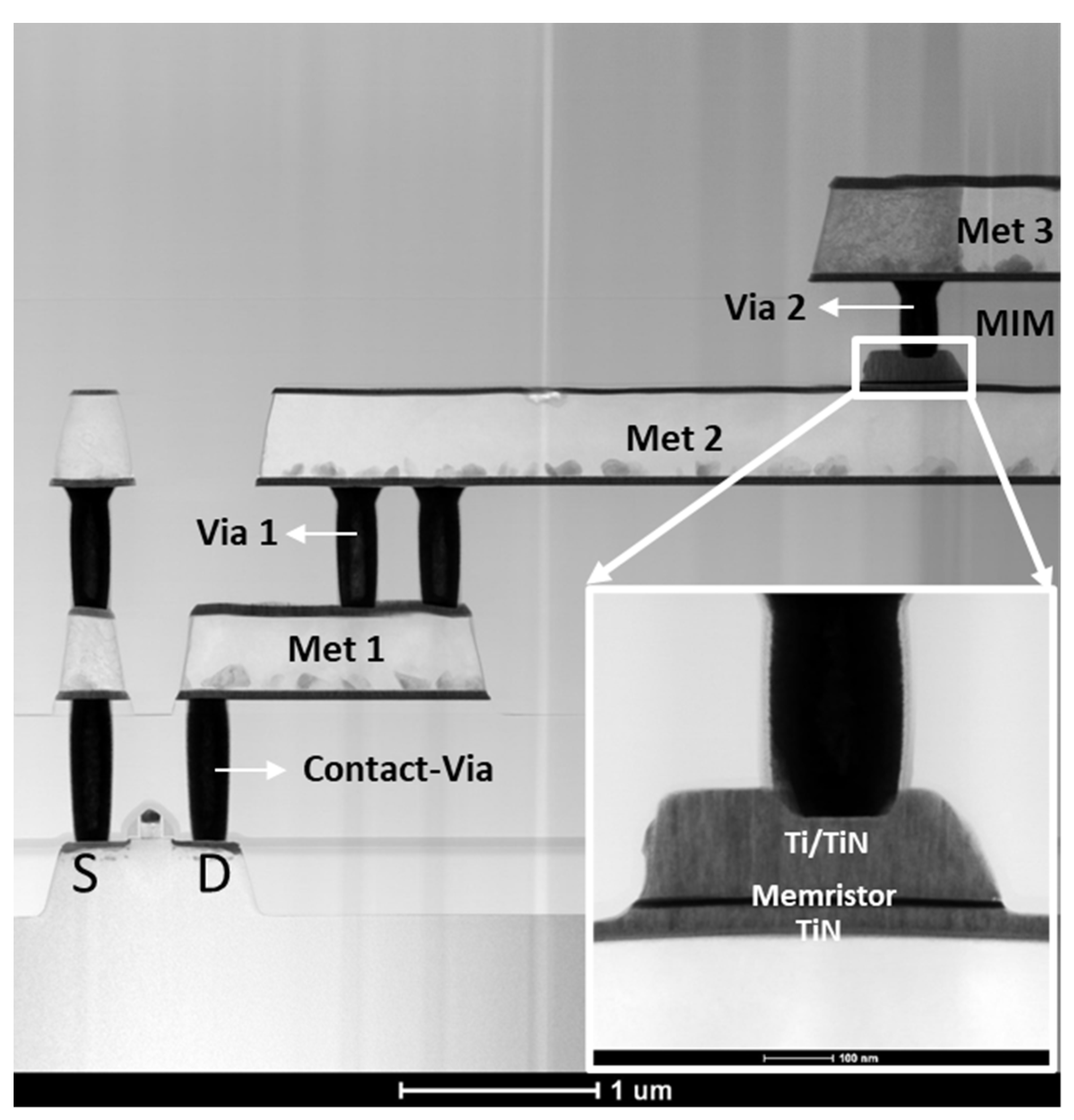
2. Experimental
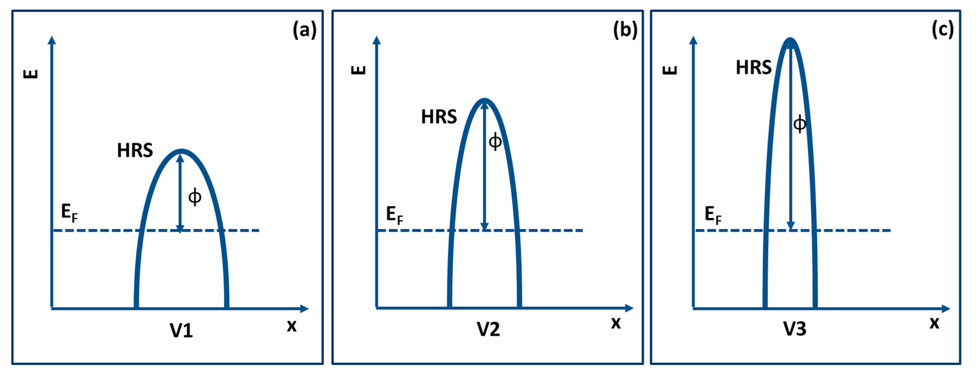
3. Quantum Point Contact (QPC) Modelling
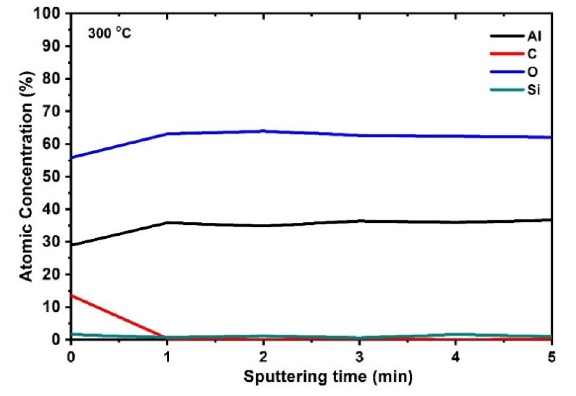
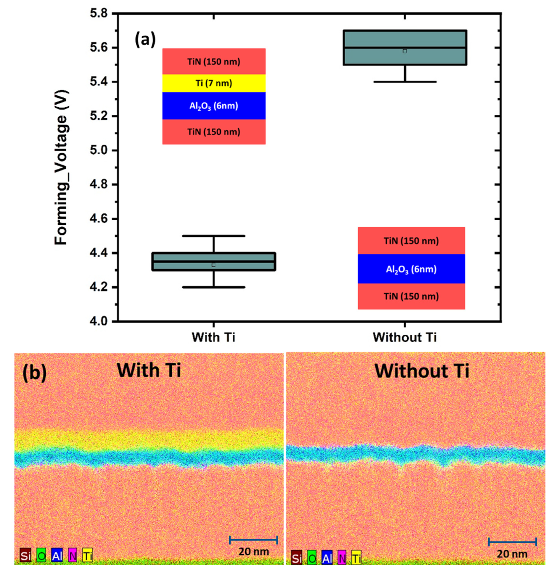
4. Results and Discussion
5. Conclusions
Author Contributions
Funding
Data Availability Statement
Acknowledgments
Conflicts of Interest
References
- Tang, X.; Giacomin, E.; Cadareanu, P.; Gore, G.; Gaillardon, P.-E. A RRAM-based FPGA for Energy-efficient Edge Computing. In Proceedings of the 2020 Design, Automation & Test in Europe Conference & Exhibition (DATE), Grenoble, France, 9–13 March 2020; pp. 144-a–144-f. [Google Scholar]
- Pastur-Romay, L.A.; Cedrón, F.; Pazos, A.; Porto-Pazos, A.B. Deep artificial neural networks and neuromorphic chips for big data analysis: Pharmaceutical and bioinformatics applications. Int. J. Mol. Sci. 2016, 17, 1313. [Google Scholar] [CrossRef] [PubMed] [Green Version]
- Brown, K.A.; Brittman, S.; Maccaferri, N.; Jariwala, D.; Celano, U. Machine Learning in Nanoscience: Big Data at Small Scales. Nano Lett. 2019, 20, 2–10. [Google Scholar] [CrossRef] [PubMed]
- Chen, Z.; Gao, B.; Zhou, Z.; Huang, P.; Li, H.; Ma, W.; Zhu, D.; Liu, L.; Liu, X.; Kang, J.; et al. Optimized learning scheme for grayscale image recognition in a RRAM based analog neuromorphic system. In Proceedings of the 2015 IEEE International Electron Devices Meeting (IEDM), Washington, DC, USA, 7–9 December 2015; p. 17. [Google Scholar]
- Krestinskaya, O.; James, A.P.; Chua, L.O. Neuromemristive Circuits for Edge Computing: A Review. IEEE Trans. Neural Netw. Learn. Syst. 2019, 31, 4–23. [Google Scholar] [CrossRef] [PubMed] [Green Version]
- Sheu, S.-S.; Cheng, K.-H.; Chang, M.-F.; Chiang, P.-C.; Lin, W.-P.; Lee, H.-Y.; Chen, P.-S.; Chen, Y.-S.; Wu, T.-Y.; Chen, F.T.; et al. Fast-write resistive RAM (RRAM) for embedded applications. IEEE Des. Test Comput. 2010, 28, 64–71. [Google Scholar] [CrossRef]
- Embedded Staff. Monolithic Embedded RRAM Presents Challenges, Opportunities. 2016. Available online: https://www.embedded.com/monolithic-embedded-rram-presents-challenges-opportunities/ (accessed on 9 January 2022).
- Yin, S.; Kim, Y.; Han, X.; Barnaby, H.; Yu, S.; Luo, Y.; He, W.; Sun, X.; Kim, J.-J.; Seo, J.-S. Monolithically Integrated RRAM- And CMOS-Based In-Memory Computing Optimizations for Efficient Deep Learning. IEEE Micro 2019, 39, 54–63. [Google Scholar] [CrossRef]
- Levisse, A.; Giraud, B.; Noel, J.-P.; Moreau, M.; Portal, J.-M. RRAM Crossbar Arrays for Storage Class Memory Applications: Throughput and Density Considerations. In Proceedings of the 2018 Conference on Design of Circuits and Integrated Systems (DCIS), Lyon, France, 14–16 November 2018; pp. 1–6. [Google Scholar] [CrossRef] [Green Version]
- Mahadevaiah, M.; Perez, E.; Wenger, C.; Grossi, A.; Zambelli, C.; Olivo, P.; Zahari, F.; Kohlstedt, H.; Ziegler, M. Reliability of CMOS Integrated Memristive HfO2 Arrays with Respect to Neuromorphic Computing. In Proceedings of the 2019 IEEE International Reliability Physics Symposium (IRPS), Monterey, CA, USA, 31 March–4 April 2019; pp. 1–4. [Google Scholar] [CrossRef]
- Gergel-Hackett, N.; Tedesco, J.L.; Richter, C.A. Memristors With Flexible Electronic Applications. Proc. IEEE 2012, 100, 1971–1978. [Google Scholar] [CrossRef]
- Gergel-Hackett, N.; Hamadani, B.; Dunlap, B.; Suehle, J.; Richter, C.; Hacker, C.; Gundlach, D. A Flexible Solution-Processed Memristor. IEEE Electron Device Lett. 2009, 30, 706–708. [Google Scholar] [CrossRef]
- Yun, H.-W.; Woo, H.K.; Oh, S.J.; Hong, S.-H. Flexible NiO nanocrystal-based resistive memory device fabricated by low-temperature solution-process. Curr. Appl. Phys. 2020, 20, 288–292. [Google Scholar] [CrossRef]
- Seo, J.W.; Park, J.-W.; Lim, K.S.; Kang, S.J.; Hong, Y.H.; Yang, J.H.; Fang, L.; Sung, G.Y.; Kim, H.-K. Transparent flexible resistive random-access memory fabricated at room temperature. Appl. Phys. Lett. 2009, 95, 133508. [Google Scholar]
- Basnet, P.; Pahinkar, D.G.; West, M.P.; Perini, C.J.; Graham, S.; Vogel, E.M. Vogel, Substrate dependent resistive switching in amorphous-HfO x memristors: An experimental and computational investigation. J. Mater. Chem. C 2020, 8, 5092–5101. [Google Scholar] [CrossRef] [Green Version]
- Almeida, S.; Aguirre, B.; Marquez, N.; McClure, J.; Zubia, D. Resistive Switching of SnO2 Thin Films on Glass Substrates. Integr. Ferroelectr. 2011, 126, 117–124. [Google Scholar] [CrossRef]
- Sophocleous, M.; Mohammadian, N.; Majewski, L.A.; Georgiou, J. Solution-processed, low voltage tantalum-based memristive switches. Mater. Lett. 2020, 269, 127676. [Google Scholar] [CrossRef]
- Rasool, A.; Amiruddin, R.; Mohamed, I.R.; Kumar, M.S. Fabrication and characterization of resistive random access memory (ReRAM) devices using molybdenum trioxide (MoO3) as switching layer. Superlattices Microstruct. 2020, 147, 106682. [Google Scholar] [CrossRef]
- Woo, J.; Yu, S. Resistive Memory-Based Analog Synapse: The Pursuit for Linear and Symmetric Weight Update. IEEE Nanotechnol. Mag. 2018, 12, 36–44. [Google Scholar] [CrossRef]
- Mahadevaiah, M.K.; Perez, E.; Wenger, C. Influence of specific forming algorithms on the device-to-device variability of memristive Al-doped HfO2 arrays. J. Vac. Sci. Technol. B Nanotechnol. Microelectron. Mater. Process. Meas. Phenom. 2020, 38, 013201. [Google Scholar] [CrossRef]
- Sokolov, A.S.; Jeon, Y.-R.; Kim, S.; Ku, B.; Lim, D.; Han, H.; Chae, M.G.; Lee, J.; Gil Ha, B.; Choi, C. Influence of oxygen vacancies in ALD HfO2−x thin films on non-volatile resistive switching phenomena with a Ti/HfO2−x/Pt structure. Appl. Surf. Sci. 2018, 434, 822–830. [Google Scholar] [CrossRef]
- Duncan, D.; Magyari-Kope, B.; Nishi, Y. Ab-Initio Modeling of the Resistance Switching Mechanism in RRAM Devices: Case Study of Hafnium Oxide (HfO2). MRS Proc. 2012, 1430. [Google Scholar] [CrossRef]
- Huang, C.-Y.; Jieng, J.-H.; Jang, W.-Y.; Lin, C.-H.; Tseng, T.-Y. Improved Resistive Switching Characteristics by Al2O3 Layers Inclusion in HfO2-Based RRAM Devices. ECS Solid State Lett. 2013, 2, P63–P65. [Google Scholar] [CrossRef]
- Fantini, A.; Goux, L.; Clima, S.; Degraeve, R.; Redolfi, A.; Adelmann, C.; Polimeni, G.; Chen, Y.Y.; Komura, M.; Belmonte, A.; et al. Engineering of Hf1xAlxOy amorphous dielectrics for high-performance RRAM applications. In 2014 IEEE 6th International Memory Workshop (IMW); IEEE: Piscataway, NJ, USA, 2014; pp. 1–4. [Google Scholar] [CrossRef]
- Chen, Y.Y.; Roelofs, R.; Redolfi, A.; Degraeve, R.; Crotti, D.; Fantini, A.; Clima, S.; Govoreanu, B.; Komura, M.; Goux, L.; et al. Tailoring switching and endurance/retention reliability characteristics of HfO2/Hf RRAM with Ti, Al, Si dopants. In Proceedings of the 2014 Symposium on VLSI Technology (VLSI-Technology): Digest of Technical Papers, Honolulu, HI, USA, 9–12 June 2014; pp. 1–2. [Google Scholar] [CrossRef]
- Wong, H.S.P.; Lee, H.Y.; Yu, S.; Chen, Y.S.; Wu, Y.; Chen, P.S.; Lee, B.; Chen, F.T.; Tsai, M.J. Metal–oxide RRAM. Proc. IEEE 2012, 100, 1951–1970. [Google Scholar] [CrossRef]
- Huang, X.; Wu, H.; Gao, B.; Sekar, D.C.; Dai, L.; Kellam, M.; Bronner, G.; Deng, N.; Qian, H. HfO2/Al2O3multilayer for RRAM arrays: A technique to improve tail-bit retention. Nanotechnology 2016, 27, 395201. [Google Scholar] [CrossRef]
- Li, J.; Zhang, T.; Duan, Q.; Li, L.; Yang, Y.; Huang, R. Engineering resistive switching behavior in TaOx based memristive devices for non-von Neuman computing applications. In Proceedings of the 2018 China Semiconductor Technology International Conference (CSTIC), Shanghai, China, 11–12 March 2018; pp. 1–3. [Google Scholar] [CrossRef]
- Bousoulas, P.; Michelakaki, I.; Skotadis, E.; Tsigkourakos, M.; Tsoukalas, D. Low-Power Forming Free TiO2–x/HfO2–y/TiO2–x-Trilayer RRAM Devices Exhibiting Synaptic Property Characteristics. IEEE Trans. Electron Devices 2017, 64, 3151–3158. [Google Scholar] [CrossRef]
- Azzaz, M.; Benoist, A.; Vianello, E.; Garbin, D.; Jalaguier, E.; Cagli, C.; Charpin, C.; Bernasconi, S.; Jeannot, S.; Dewolf, T.; et al. Benefit of Al2O3/HfO2 bilayer for BEOL RRAM integration through 16kb memory cut characterization. In Proceedings of the European Solid-State Device Research Conference, Graz, Austria, 14–18 September 2015; pp. 266–269. [Google Scholar] [CrossRef]
- Yu, S.; Wu, Y.; Chai, Y.; Provine, J.; Wong, H.-S.P. Characterization of switching parameters and multilevel capability in HfOx/AlOx bi-layer RRAM devices. In Proceedings of the International Symposium on VLSI Technology, Systems, and Applications, Hsinchu, Taiwan, 25–27 April 2011; pp. 106–107. [Google Scholar] [CrossRef]
- Goux, L.; Fantini, A.; Kar, G.; Chen, Y.Y.; Jossart, N.; Degraeve, R.; Clima, S.; Govoreanu, B.; Lorenzo, G.; Pourtois, G.; et al. 2012 Symposium on VLSI Technology (VLSIT); IEEE: Honolulu HI, USA, 2014; pp. 159–160. [Google Scholar] [CrossRef]
- Woo, J.; Moon, K.; Song, J.; Lee, S.; Kwak, M.; Park, J.; Hwang, H. Improved Synaptic Behavior Under Identical Pulses Using AlOx/HfO2Bilayer RRAM Array for Neuromorphic Systems. IEEE Electron Device Lett. 2016, 37, 994–997. [Google Scholar] [CrossRef]
- Chand, U.; Huang, K.-C.; Huang, C.-Y.; Tseng, T.-Y. Mechanism of Nonlinear Switching in HfO2-Based Crossbar RRAM With Inserting Large Bandgap Tunneling Barrier Layer. IEEE Trans. Electron Devices 2015, 62, 3665–3670. [Google Scholar] [CrossRef]
- Banerjee, W.; Xu, X.; Lv, H.; Liu, Q.; Long, S.; Liu, M. Variability Improvement of TiOx/Al2O3 Bilayer Nonvolatile Resistive Switching Devices by Interfacial Band Engineering with an Ultrathin Al2O3 Dielectric Material. ACS Omega 2017, 2, 6888–6895. [Google Scholar] [CrossRef]
- Miranda, E.; Walczyk, C.; Wenger, C.; Schroeder, T. Model for the Resistive Switching Effect in HfO2 MIM Structures Based on the Transmission Properties of Narrow Constrictions. IEEE Electron Device Lett. 2010, 31, 609–611. [Google Scholar] [CrossRef]
- Lian, X.; Long, S.; Cagli, C.; Buckley, J.; Miranda, E.; Liu, M.; Sune, J. Quantum point contact model of filamentary conduction in resistive switching memories. In Proceedings of the 2012 13th International Conference on Ultimate Integration on Silicon, Grenoble, France, 5–7 of March 2012; pp. 101–104. [Google Scholar] [CrossRef]
- Prócel, L.M.; Trojman, L.; Moreno, J.; Crupi, F.; Maccaronio, V.; Degraeve, R.; Goux, L.; Simoen, E. Experimental evidence of the quantum point contact theory in the conduction mechanism of bipolar HfO2-based resistive random access memories. J. Appl. Phys. 2013, 114, 074509. [Google Scholar] [CrossRef]
- Lian, X.; Wang, M.; Rao, M.; Yan, P.; Yang, J.J.; Miao, F. Characteristics and transport mechanisms of triple switching regimes of TaOx memristor. Appl. Phys. Lett. 2017, 110, 173504. [Google Scholar] [CrossRef]
- Mahadevaiah, M.K.; Lisker, M.; Fraschke, M.; Marschmeyer, S.; Schmidt, D.; Wenger, C.; Perez, E.; Mai, A. (Invited) Optimized HfO2-Based MIM Module Fabrication for Emerging Memory Applications. ECS Trans. 2019, 92, 211–221. [Google Scholar] [CrossRef]
- Puurunen, R.L. Surface chemistry of atomic layer deposition: A case study for the trimethylaluminum/water process. J. Appl. Phys. 2005, 97, 121301. [Google Scholar] [CrossRef]
- Jakschik, S.; Schroeder, U.; Hecht, T.; Gutsche, M.; Seidl, H.; Bartha, J.W. Crystallization behavior of thin ALD-Al2O3 films. Thin Solid Films 2003, 425, 216–220. [Google Scholar] [CrossRef]
- Knoops, H.C.M.; Potts, S.E.; Bol, A.A.; Kessels, W.M.M. Atomic layer deposition. In Handbook of Crystal Growth; Elsevier: Amsterdam, The Netherlands, 2015; pp. 1101–1134. [Google Scholar]
- Grossi, A.; Perez, E.; Zambelli, C.; Olivo, P.; Miranda, E.; Roelofs, R.; Woodruff, J.; Raisanen, P.; Li, W.; Givens, M.; et al. Impact of the precursor chemistry and process conditions on the cell-to-cell variability in 1T-1R based HfO2 RRAM devices. Sci. Rep. 2018, 8, 1–11. [Google Scholar] [CrossRef] [PubMed] [Green Version]
- Perez, E.; Grossi, A.; Zambelli, C.; Olivo, P.; Wenger, C. Impact of the Incremental Programming Algorithm on the Filament Conduction in HfO2-Based RRAM Arrays. IEEE J. Electron Devices Soc. 2017, 5, 64–68. [Google Scholar] [CrossRef]
- McPherson, J.W.; Kim, J.; Shanware, A.; Mogul, H.; Rodriguez, J. Trends in the ultimate breakdown strength of high dielectric-constant materials. IEEE Trans. Electron Devices 2003, 50, 1771–1778. [Google Scholar] [CrossRef]
- Sokolov, A.S.; Son, S.K.; Lim, D.; Han, H.H.; Jeon, Y.-R.; Lee, J.H.; Choi, C. Comparative study of Al2O3, HfO2, and HfAlOx for improved self-compliance bipolar resistive switching. J. Am. Ceram. Soc. 2017, 100, 5638–5648. [Google Scholar] [CrossRef]
- Pérez, E.; Pérez-Ávila, A.; Romero-Zaliz, R.; Mahadevaiah, M.; Quesada, E.P.-B.; Roldán, J.; Jiménez-Molinos, F.; Wenger, C. Optimization of Multi-Level Operation in RRAM Arrays for In-Memory Computing. Electronics 2021, 10, 1084. [Google Scholar] [CrossRef]
- Milo, V.; Anzalone, F.; Zambelli, C.; Perez, E.; Mahadevaiah, M.K.; Ossorio, O.G.; Olivo, P.; Wenger, C.; Ielmini, D. Optimized programming algorithms for multilevel RRAM in hardware neural networks. In Proceedings of the 2021 IEEE International Reliability Physics Symposium (IRPS), Monterey, CA, USA, 21–25 March 2021; pp. 1–6. [Google Scholar]
- Peng, C.-S.; Chang, W.-Y.; Lee, Y.-H.; Lin, M.-H.; Chen, F.; Tsai, M.-J.; Cho, J.-Y.; Yang, T.-Y.; Park, Y.-J.; Joo, Y.-C. Improvement of Resistive Switching Stability of HfO2 Films with Al Doping by Atomic Layer Deposition. Electrochem. Solid State Lett. 2012, 15, H88. [Google Scholar] [CrossRef]
- Yu, S.; Gao, B.; Dai, H.; Sun, B.; Liu, L.; Liu, X.; Han, R.; Kang, J.; Yu, B. Improved Uniformity of Resistive Switching Behaviors in HfO2 Thin Films with Embedded Al Layers. Electrochem. Solid State Lett. 2010, 13, H36–H38. [Google Scholar] [CrossRef]
- Grossi, A.; Zambelli, C.; Olivo, P.; Miranda, E.; Stikanov, V.; Schroeder, T.; Walczyk, C.; Wenger, C. Relationship among Current Fluctuations during Forming, Cell-To-Cell Variability and Reliability in RRAM Arrays. In Proceedings of the 2015 IEEE International Memory Workshop (IMW), Monterey, CA, USA, 17–20 May 2015. [Google Scholar] [CrossRef] [Green Version]
- Grossi, A.; Zambelli, C.; Olivo, P.; Crespo-Yepes, A.; Martin-Martinez, J.; Rodríguez, R.; Nafria, M.; Perez, E.; Wenger, C. Electrical characterization and modeling of 1T-1R RRAM arrays with amorphous and poly-crystalline HfO2. Solid State Electron. 2017, 128, 187–193. [Google Scholar] [CrossRef] [Green Version]
- Lian, X.; Cartoixà, X.; Miranda, E.; Perniola, L.; Rurali, R.; Long, S.; Liu, M.; Suñé, J. Multi-scale quantum point contact model for filamentary conduction in resistive random access memories devices. J. Appl. Phys. 2014, 115, 244507. [Google Scholar] [CrossRef]


| Description | V1 (nm) | V2 (nm) | V3 (nm) |
|---|---|---|---|
| TiN TE | 150 | 150 | 150 |
| Ti | 7 | 7 | 7 |
| HfO2 | 8 | 8 | 8 |
| Al2O3 | - | 1 | 2 |
| TiN BE | 150 | 150 | 150 |
| Description | V1 | V2 | V3 |
|---|---|---|---|
| Mean LRS (A) | 1.61 × 10⁻⁵ | 2.35 × 10⁻⁵ | 2.63 × 10⁻⁵ |
| Mean HRS (A) | 1.88 × 10⁻⁷ | 3.2 × 10⁻⁷ | 4.23 × 10⁻⁷ |
| MW (Mean LRS/Mean HRS) | ~86 | ~73 | ~62 |
| Description | N |
|---|---|
| V1 | 1.43 |
| V2 | 2.33 |
| V3 | 2.73 |
| Description | α | φ | TB/RB |
|---|---|---|---|
| V1 | 17.61 | 0.29 | 1.35 |
| V2 | 8.37 | 0.53 | 1.17 |
| V3 | 6.75 | 0.6 | 1.07 |
Publisher’s Note: MDPI stays neutral with regard to jurisdictional claims in published maps and institutional affiliations. |
© 2022 by the authors. Licensee MDPI, Basel, Switzerland. This article is an open access article distributed under the terms and conditions of the Creative Commons Attribution (CC BY) license (https://creativecommons.org/licenses/by/4.0/).
Share and Cite
Kalishettyhalli Mahadevaiah, M.; Perez, E.; Lisker, M.; Schubert, M.A.; Perez-Bosch Quesada, E.; Wenger, C.; Mai, A. Modulating the Filamentary-Based Resistive Switching Properties of HfO2 Memristive Devices by Adding Al2O3 Layers. Electronics 2022, 11, 1540. https://doi.org/10.3390/electronics11101540
Kalishettyhalli Mahadevaiah M, Perez E, Lisker M, Schubert MA, Perez-Bosch Quesada E, Wenger C, Mai A. Modulating the Filamentary-Based Resistive Switching Properties of HfO2 Memristive Devices by Adding Al2O3 Layers. Electronics. 2022; 11(10):1540. https://doi.org/10.3390/electronics11101540
Chicago/Turabian StyleKalishettyhalli Mahadevaiah, Mamathamba, Eduardo Perez, Marco Lisker, Markus Andreas Schubert, Emilio Perez-Bosch Quesada, Christian Wenger, and Andreas Mai. 2022. "Modulating the Filamentary-Based Resistive Switching Properties of HfO2 Memristive Devices by Adding Al2O3 Layers" Electronics 11, no. 10: 1540. https://doi.org/10.3390/electronics11101540
APA StyleKalishettyhalli Mahadevaiah, M., Perez, E., Lisker, M., Schubert, M. A., Perez-Bosch Quesada, E., Wenger, C., & Mai, A. (2022). Modulating the Filamentary-Based Resistive Switching Properties of HfO2 Memristive Devices by Adding Al2O3 Layers. Electronics, 11(10), 1540. https://doi.org/10.3390/electronics11101540