Review

In-Memory Computing with Resistive Memory Circuits: Status and Outlook

Dipartimento di Elettronica, Informazione e Bioingegneria, Politecnico di Milano and IU.NET, 20133 Milano, Italy
*
Author to whom correspondence should be addressed.
Electronics 2021, 10(9), 1063; https://doi.org/10.3390/electronics10091063
Submission received: 1 April 2021 / Revised: 24 April 2021 / Accepted: 26 April 2021 / Published: 30 April 2021
(This article belongs to the Special Issue High-Density Solid-State Memory Devices and Technologies)

Abstract

:
In-memory computing (IMC) refers to non-von Neumann architectures where data are processed in situ within the memory by taking advantage of physical laws. Among the memory devices that have been considered for IMC, the resistive switching memory (RRAM), also known as memristor, is one of the most promising technologies due to its relatively easy integration and scaling. RRAM devices have been explored for both memory and IMC applications, such as neural network accelerators and neuromorphic processors. This work presents the status and outlook on the RRAM for analog computing, where the precision of the encoded coefficients, such as the synaptic weights of a neural network, is one of the key requirements. We show the experimental study of the cycle-to-cycle variation of set and reset processes for HfO 2 -based RRAM, which indicate that gate-controlled pulses present the least variation in conductance. Assuming a constant variation of conductance σ G , we then evaluate and compare various mapping schemes, including multilevel, binary, unary, redundant and slicing techniques. We present analytical formulas for the standard deviation of the conductance and the maximum number of bits that still satisfies a given maximum error. Finally, we discuss RRAM performance for various analog computing tasks compared to other computational memory devices. RRAM appears as one of the most promising devices in terms of scaling, accuracy and low-current operation.

1. Introduction

According to More’s law, novel computing concepts are being researched to mitigate the memory bottleneck typical of von Neumann architectures. Among these new concepts, in-memory computing (IMC) has attracted an increasing interest due to the ability to execute computing tasks directly within the memory array [1,2,3]. Various IMC circuits have been proposed so far, including digital gates [4,5,6,7], physical unclonable functions (PUF) [8,9,10,11] and neuromorphic neurons and synapses [12,13,14,15,16]. In these circuits, the computational function stems from a physical property of the memory device and circuit, such as set/reset dynamics of resistive switching memory (RRAM) for synaptic potentiation/depression and neuron integration and fire. As a result of the physics-based computation, most IMC circuits operate in the analog domain and in a continuous time scale. A typical example of analog IMC primitive is the matrix vector multiplication (MVM), which can be executed in one step in a crosspoint memory array [17,18,19]. The parallel and analog IMC operation allows the MVM operation to be significantly sped up with respect to the conventional multiply-accumulate (MAC) algorithm of digital computers [20,21]. Crosspoint-based MVM has been adopted in a number of computing applications, ranging from deep neural networks (DNNs) [22,23,24,25] to linear algebra accelerators [26,27,28,29].
Figure 1 illustrates the hierarchical design approach for IMC accelerators. Computation is enabled at the device level by transport phenomena, e.g., the Ohm’s law enabling multiplication of voltage and conductance or the threshold switching enabling comparison between voltages [30]. Devices are connected within circuits, allowing parallel flow of input and output signals, Kirchhoff’s current summation and feedback connections, usually in the analog domain. Circuit primitives are organized within novel architectures to harness the full potential of the computing cores and accelerate data-intensive workloads such as neural networks. Based on such a hierarchical structure, it is clear that the proper optimization of the analog accelerators requires a co-design approach from materials to applications to take into account device characteristics, circuit/device non-idealities and possible architecture limitations. Algorithms such as training of neural networks can also be used to optimize precision in view of device and circuit non-idealities. In this regard, a key point is the precision of the physical representation or mapping of the computational coefficients and the overall computation, which might be affected by noise, instability and parasitic elements in the crosspoint array circuit [31].
This work presents an overview of analog IMC with RRAM devices. We first address the programming characteristics of a typical HfO 2 RRAM devices to highlight the intrinsic conductance variations for various programming algorithms. Then we focus on the various options for mapping computational parameters, such as synaptic weights in a DNN, discussing the trade-off between precision and memory area. Finally, we extend our study to various memory parameters, including low-current operation, programming speed and cycling endurance, by discussing their importance for various computational applications and the memory devices that maximize these performance metrics.

2. RRAM Device Structure

Various nanoscale devices have been proposed as a new class of non-volatile memory, where information is stored as the physical configuration of active material, resulting in different conductance [1]. For example, information can be stored and retrieved by the device spin magnetization in a magnetic random access memory (MRAM) [32], as the phase structure of the materials in phase change memories [33,34] or as the atomic configuration of conductive defects in resistive switching memories, or RRAM [35]. The latter has attracted particular interest thanks to the simple structure, compatibility with CMOS process, fast operation and high density [36,37]. Figure 2a shows the typical structure and operation of a RRAM device, consisting of an insulating metal-oxide layer interposed between a metallic top electrode (TE) and a metallic bottom electrode (BE). The insulating layer results in a typical high resistance following fabrication. A forming process consisting of the application of a relatively high positive voltage pulse on the TE induces a local modification of the material composition with the growth of a metallic filament resulting in the low resistance state (LRS). A high resistance state (HRS) can be recovered by means of a negative voltage applied to the TE, which results in the creation of a depletion region across the conductive filament, thus resulting in a decrease of conductance. In addition to the LRS and the HRS intermediate states can be programmed. Thus it is possible, e.g., by controlling the filament size via the maximum current flowing across the device during the set operation, i.e., the compliance current I C . This is relatively straightforward in the 1-transistor-1-resistor (1T1R) structure as shown in the inset Figure 2b, or by controlling the maximum voltage applied during the reset operation which results in a different thickness of the depletion gap. For instance, Figure 2b shows typical current-voltage (I-V) curves of a RRAM device in 1T1R configuration for increasing I C , controlled with the transistor gate voltage V G [38], demonstrating the possibility of analog programming.
The multilevel cell (MLC) capability of Figure 2b is interesting not only for increasing the bit density of the memory, but also for enabling computing applications [39]. In fact, by arranging RRAM in crosspoint configuration as shown in Figure 3, it is possible to directly encode arbitrary matrix entry A i j into the conductance value G i j [1,31]. Then, by applying a voltage vector V as input on the columns and collecting the current flowing in each row I j , it is possible to compute the matrix vector multiplication (MVM) according to:
I j = i = 1 N G i j V i
where N is the dimension of the input vector, thus G is a N × N matrix. MVM is at the backbone of a variety of data-intensive applications that can be accelerated by IMC acceleration, such as neural network training and inference [40,41,42,43], neuromorphic computing [15,16,44,45], image processing [18,46], optimization problems [47,48,49,50] and the iterative solution of linear equations [26,27]. Circuits able of solving matrix equations without iteration thanks to analog feedback have also been demonstrated [28,29,38]. All these applications have in common the need for reliable analog memory, which still appears a challenge due to the inherent stochasticity of switching behavior in RRAM devices.

3. Analog Memory Programming Techniques and Variations

Programming the same device several times, in the same condition (or initial state) of programming pulse-width and amplitude, results in various conductance due to the stochastic process of ionic migration during set/reset operation, which is usually referred to as cycle-to-cycle variability [35]. Figure 4a shows an example of a programming algorithm during set operation, namely incremental gate pulse programming (IGPP), where the TE voltage V T E is kept constant while the gate voltage V G is increased at each time step. This process was repeated 1200 times and the conductance was read with a relatively low voltage after each cycle [51]. Figure 4b shows that the single traces (grey) suffer from relatively large variations, while the median value (blue) seems to grow linearly with pulse number (i.e., V G ). The cumulative distribution of the conductance for each cycle is reported in Figure 4c for increasing V G . The standard deviation of the conductance σ G as a function of the median conductance is reported in Figure 4d, indicating a fairly constant value σ G = 3.8 μ S. This indicates a linear increase in relative resistance variation σ R / R with resistance R, since R = 1 / G and, on a first approximation, variations obey the same relationship between differential quantities, hence σ R / R = σ G / G [35]. The linear increase in σ R with R is generally observed in variability measurements of RRAM [52,53] and has been attributed to variation in the shape of the conductive filament. Other variability data have been reported indicating an increase in σ R / R as R 0.5 , which can be interpreted in terms of Poissonian variation of the number of defects in the conductive filament [54,55,56].
Analog programming of RRAM is also possible in the opposite polarity, namely by increasing the negative reset voltage V T E applied on the TE for a fixed V G , an algorithm referred to as incremental reset pulse programming (IRPP), as shown in Figure 5a. In this case, by first initializing the conductance into the LRS, it is possible to characterize the variability of analog programming with reset voltage by applying IRPP several times (i.e., 1200 as in Figure 5) [51]. Figure 5b again evidences that single traces (grey) corresponding to conductance read after each pulse of a single reset ramp, show high variability and fluctuation, while the median value (blue) shows a gradual decrease with the pulse number. The cumulative distributions of such conductance are reported in Figure 5c for increasing applied TE voltage | V S T O P | . The resulting standard deviation of conductance σ G as a function of median conductance G is shown in Figure 5d (red): from the comparison with IGPP results of Figure 5 (blue), it is possible to see that σ G is generally larger in the reset process. We can conclude that gradual set programming is more convenient than gradual reset for accurate tuning of resistance; however, accurate program/verify (PV) algorithms are needed for reducing the error to acceptable levels (i.e., for having σ G < 1 μ S).

3.1. Program-Verify Algorithms and Device-to-Device Variations

To date, only cycle-to-cyle variation on a single device was considered. To address device-to-device variation, conductance is typically characterized in a relatively large array (e.g., >1 kB), which allows one to study the main variability features with a relatively simple circuit and short experimental time. Figure 6a illustrates a conceptual schematic of a PV algorithm for 1T-1R RRAM, namely incremental-step program-verify algorithm (ISPVA) [43] applied on a 4 kB array. For a given V G (or I C ), the TE is incremented until the read value of G after programming reaches the target value G = L i . Figure 6b shows conductance traces as a function of V T E for increasing V G obtained with ISPVA for target levels L 2 5 . The experiment was repeated on all the devices in the array, and the read current probability distributions are shown in Figure 6d [43]. The final average standard deviation is σ G = 7.5 μ S, which is slightly larger than the case of Figure 4 despite the PV algorithm where the number of pulses is adapted to reach a certain conductance. The larger σ G can be understood by the superposition of cycle-to-cycle variation and device-to-device variation, the latter having the larger contribution to variability within the array.

3.2. Conductance Drift and Fluctuations

Unfortunately, once the device is programmed with a given precision, the conductance might still change due to time-dependent drift and fluctuation that affects the reliability of IMC. Figure 7a shows measured traces of conductance programmed with 4 levels on a 1Mb RRAM array as a function of time during annealing at 150 °C [58]. The change of conductance can be explained by the thermally-activated atomic diffusion in the conductive filament. Note that, in addition to conductance drift with time, random fluctuations across the median value are present, as shown in Figure 7a. This is better illustrated in Figure 7b [59], where the resistance of a RRAM device in HRS is plotted as a function of time. The results show that the resistance can experience abrupt variations, called random walk, in addition to the typical random telegraph noise (RTN). For instance, the accuracy of neural network can decrease with time due to the introduction of a bias in the conductance as a result of the drift [43,58,60]. Figure 7c shows the cumulative distribution of the initial and drifted conductance by annealing at T = 125 °C of Figure 6c [43], which confirms the time-dependent drift of weights of a two-layer neural network. The network schematic is represented in Figure 7d, and it is composed of a 14 × 14 input layer (corresponding to a downsized version of the MNIST dataset), a hidden layer of 20 neurons and 10 output neurons corresponding to 10 handwritten digits and resulting in a total of 14 × 14 × 20 + 20 × 10 weights, which can be mapped in a 4 kB array. Figure 7e shows the confusion map for testing the MNIST dataset before annealing, showing a relatively good average accuracy of 83%. However, this accuracy drops to 72% after annealing as shown in Figure 7f, demonstrating the need of stable states for reliable neural network inference.

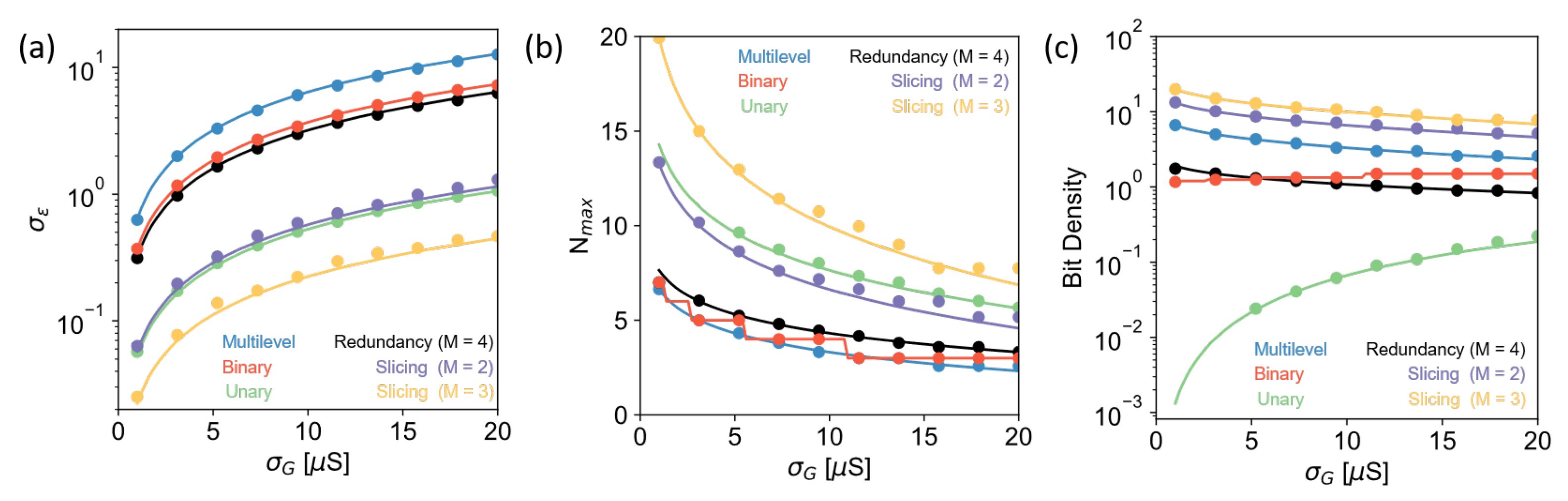
4. RRAM Conductance Mapping Techniques

While Figure 2, Figure 3, Figure 4 and Figure 5 focus on multilevel conductance mapping, aiming at an increase in the number of programmable levels and a reduction of the programming error, other techniques can be adopted to map a given computing coefficient, such as a synaptic weight, into one or multiple memory devices. Figure 8 summarizes the main programming methodologies for IMC [51], including multilevel (a) [43,61], binary (b) [62], unary (c) [63], multilevel with redundancy (d) [64] and slicing (e) [23]. In the following, we compare the various techniques in terms of mapping accuracy, maximum number of bits and number of devices. The mapping accuracy is evaluated by the standard deviation of the error σ ϵ in programming a certain coefficient with a given number of bits N. The accuracy is evaluated by analytical formulas assuming a constant σ G in programming an individual memory device with a maximum conductance G m a x [51].

4.1. Multilevel

Analog memories can naturally map discretized levels, which is referred to as multilevel mapping. To store N bits, 2 N equally spaced conductance levels between 0 and G m a x are needed. As a result, each level is separated from the adjacent ones by a conductance step Δ G = G m a x / ( 2 N 1 ) . Given a standard deviation of the programming error σ G , such as the value σ G = 3.8 μ S in Figure 4d, the resulting standard deviation σ ϵ of the error in programming N bits can be obtained as:
σ ϵ = σ G Δ G = ( 2 N 1 ) σ G G m a x .
Equation (2) allows one to estimate the maximum number of bits N m a x , which can be mapped in a RRAM device with a given acceptable error σ ϵ < < 1 , which yields N m a x = l o g 2 ( 1 + σ ϵ G m a x / σ G ) . For example, by considering σ G = 2.2 μ S , G m a x = 225 μ S [57] and targeting a maximum error of σ ϵ = 10 % , the resulting maximum number of bits is N m a x = 3.35 corresponding to 10 levels that can be written in the memory to satisfy the precision requirement.

4.2. Binary

Binary storage is the typical mapping of conventional digital memories, where a value x is converted in its binary representation with N bits written in N memory cells, each containing two states for 0 and 1. For instance, x = 14 can be written in binary representation as x b i n = 1110 with 4 RRAM cells programmed to [ G m a x , G m a x , G m a x , 0 ] , respectively. A weighted summation of the conductance values is possible by multiplying the current flowing in each cell by the corresponding power of 2, namely 2 3 , 2 2 , 2 1 , 2 0 , respectively, thus allowing one to reconstruct the correct number as [ 2 3 + 2 2 + 2 1 ] V r e a d G m a x = 14 V r e a d G m a x . To estimate σ ϵ , we consider the average imprecision divided by the least significant bit (LSB), namely:
σ ϵ = 1 G m a x i = 0 N 1 2 2 i σ G 2 = σ G G m a x 2 2 N 1 3 ,
where the square-root term combines the independent variation of each memory cell multiplied by its weight. The maximum number of bits thus can be obtained as:
N = 1 2 l o g 2 1 + 3 G m a x σ ϵ σ G 2 .
Assuming the same σ G , G m a x and σ ϵ of the estimation for multilevel mapping, we obtain N m a x = 4.15 with binary RRAM.

4.3. Unary

To increase the precision of binary mapping, unary (or thermometric) coding uses 2 N 1 devices to represent the information, each one having equal weight, which requires no bit-specific gain in the current summation. In unary coding, the error is given by:
σ ϵ = σ G G m a x 2 N 1
which leads to a N m a x = 7.7 with the same σ G , G m a x and σ ϵ used in the previous estimation. However, note that the higher precision has been achieved at the cost of a larger number of RRAMs, namely 2 N m a x 1 = 207 memory devices.

4.4. Multilevel with Redundancy

To reduce the impact of σ G on multilevel coding, M memory devices having the same nominal conductance can be programmed and operated in parallel. As a result, the error is reduced by a factor M thanks to the averaging among the M redundant cells (see Table 1). The maximum number of bits is equivalently enhanced. Assuming M = 4 and the same σ G , G m a x and σ ϵ used in the previous estimation, we obtain N m a x = 4.36 bits, i.e., one additional bit compared to the pure multilevel case with no redundancy.

4.5. Slicing

By encoding a given number in base l, with l = 2 N number of levels stored in a single memory element with multilevel mapping, and using M different memories to represent the data, it is possible to significantly increase the precision in a compact implementation. For example, x = 14 encoded in base l = 4 yields to x 4 = 32 such that by using two memory elements with weights 4 1 and 4 0 , the current summation yields x = 4 1 × 3 + 4 0 × 2 . Slicing can thus increase the number of addressable levels l by the number of used cells. The error can be evaluated in the same way as the binary scheme, by summing the weighted error contribution of each cell, which yields:
σ ϵ = σ G G m a x 1 + 2 2 N M 1 .
Assuming M = 4 and the same values of σ G , G m a x and σ ϵ as before, we obtain N m a x = 13.41 bits for slicing.

4.6. Simulation Results

Table 1 summarizes the formulas for calculating the error σ ϵ and the maximum number of bits N m a x for different programming techniques. To validate the analytical formulas, we performed Monte Carlo simulations of the various programming conditions and compared the results to the analytical calculations [51].
Table 1. Comparison of various mapping schemes, in terms of conductance range, variability-induced error and resulting maximum number of programmable bits.
Technique G range σ ϵ N max
Multilevel G m a x 2 N σ G G m a x l o g 2 ( σ ϵ G m a x σ G )
Binary ( 2 N 1 ) G m a x 2 2 N 1 3 σ G G m a x l o g 2 1 + 3 σ ϵ G m a x σ G 2 / 2
Unary ( 2 N 1 ) G m a x 2 N 1 σ G G m a x 2 l o g 2 ( σ ϵ G m a x σ G ) + 1
Multilevel
with redundancy
M G m a x 2 N σ G G m a x M l o g 2 ( σ ϵ G m a x M σ G )
Slicing ( 2 M N 1 ) G m a x 1 + 2 2 N M 1 σ G G m a x M 2 1 + l o g 2 σ ϵ 2 G m a x 2 σ G 2 1
Figure 9 shows the results of the analytical formulas (top) compared with the results of MC simulations (bottom) for the standard deviation of the error σ ϵ as a function of the standard deviation of conductance σ G and the number of bits to encode N, for multilevel (a,f), binary (b,g), unary (c,h), multilevel with redundancy M = 4 (d,i) and slicing with M = 2 (e,j) [51]. The analytical formulas and the MC simulations show a good agreement, thus confirming the correctness of the models in Table 1.
Figure 10a shows the calculated σ ϵ as a function of σ G for a target number N = 7 of bits. The results indicate that slicing and unary programming have a significant advantage over the other techniques by approximately one order of magnitude. This result is confirmed in Figure 10b showing the maximum number of bits N m a x as a function of σ G for σ ϵ = 1 % . However, unary and slicing techniques require several memory elements to encode the coefficients, which thus increase the energy consumption and chip area per bit. To address the precision/area trade-off, Figure 10c shows the bit density, evaluated as N m a x divided by the number of memory cells as a function of σ G . The results demonstrate the good trade-off for the case of the slicing technique.

5. Array-Level Reliability Issues

Device variations and errors are not the only origin for accuracy degradation in IMC circuits. In large memory arrays, the interconnect lines are generally affected by non-ideal behavior due to the parasitic resistance and capacitance that can deteriorate the analog signal integrity. In particular, parasitic wire resistance introduces a significant error, due to the current-resistance (IR) drop on the array rows/columns, which results in a difference between the applied voltage and the one across each memory cell. Figure 11a shows a sketch of a 4 × 4 memory array highlighting the wire resistance, namely the input resistance R i n , the output resistance R o u t and the row/column wire resistance r between each memory cell [65]. Assuming for instance an inference operation with a typical read voltage V r e a d = 0.1 V, an average RRAM resistance R = 100 k Ω , corresponding to a current I = 100   μ A for each cell within a a 100 × 100 crosspoint array with wire resistance r = 1 Ω , then the overall IR drop can be computed as r I + 2 r I + 3 r I + + N r I = r I N 2 2 = 5 mV corresponding to a 5 % error in the summation current [66]. Note that this error does not include any contribution due to variations in RRAM conductance.
To mitigate this effect, it is possible to increase the device resistance to decrease the current at the array wires. Unfortunately, large device resistances are usually more prone to variations, drift, fluctuations and noise [52,55]. Furthermore, a high cell resistance requires a longer readout time because of CMOS noise in the sensing circuit, thus resulting in longer program/verify algorithms. Finally, the higher cell resistance could increase the R C delay time for charging the BL. IR drop can be mitigated by changing the memory device topology, for example, by inserting a current-controlled synaptic element [67], such as a Flash memory, ionic transistor or FeFET, as shown in Figure 11b. A three-terminal memory transistor can be programmed to various saturation currents, each representing a synaptic weight. By encoding the input in the gate pulsewidth and integrating the current flowing in each column, it is possible to perform a current-based computation where the resulting charge is given by:
Q i = j = 1 N i i j t j
which corresponds to a MVM of a current matrix times a pulsewidth vector. Figure 11c shows a a comparison of the impact of IR drop for ohmic and saturated characteristics, demonstrating a much smaller impact of the current controlled devices [67].
At algorithmic level, IR drop and other non-idealities can be taken into account during training/inference or programming of computational memory devices. For instance, parasitic-aware program-and-verify algorithms have been presented to minimize the impact of IR drop [65,68]. By iteratively programming the target conductance matrix G resulting in G , evaluating the current i = V G and comparing it to the ideal current i = v G , a new target matrix can be computed and programmed. The algorithm is repeated until the error is reduced below a certain tolerance, e.g., ϵ = | i i | < 1 % .
At circuit architecture level, various techniques have been proposed to mitigate the impact of IR drop. Typically, the synaptic weights in a neural network have a differential structure, thus two separate 1T1R memory devices are used for representing a single weight. This is shown in Figure 12a where two contiguous columns are used for representing positive and negative weights that are summed up in the digital domain [69]. This configuration results in a relatively large impact of the IR drop since two array locations are used for each matrix entry. To mitigate this issues, Figure 12b shows a signed-weighted 2-transistor/2-resistor (SW-2T2R) structure to represent the positive and negative part of each weight, where the current summation is performed directly within the memory cell, thus effectively reducing the impact of IR drop by roughly a factor 2 [69]. Another approach is to use small-size crosspoint arrays and/or organize the IMC architecture in computing tiles [70,71], where the overall problem is divided in smaller operations with smaller summation currents, hence a lower IR drop.

6. Circuit Primitives for Analog Computing

Various computing primitives based on similar array organization of memory devices have been proposed. Figure 13 summarizes the main circuit primitives, including the MVM accelerator [1,18,22,26,27,42,46,47,48,49,65], the closed-loop circuit for inverse algebra problems [28,29,38] and the analog content addressable memory (CAM) [72,73].

6.1. MVM Accelerator

Figure 13a shows a circuit schematic for implementing the MVM accelerator of Equation (1). The conductance matrix G is stored in the RRAM device of the crosspoint array and the input voltage vector V is applied with a digital-to-analog converter (DAC) connected to the rows of the array. Columns are connected to the sensing circuit, consisting of a trans-impedance amplifier (TIA) that converts currents into voltages, and an analog-to-digital converter (ADC), which encodes the analog signals into digital words. MVM is performed in a single step, irrespective of the matrix size, although typically the sensing operation is multiplexed between various columns to reduce the peripheral overhead [60]. Since the forward propagation in a neural networks basically consists in extensive MVM of activation signal multiplied by synaptic weights [74], MVM crosspoint circuits have been heavily used for accelerating both the inference [22,43] and the training [41,42] stage of neural networks. Since the neuron activation function is typically performed in the digital domain, various training algorithms have been developed, including supervised training [42], unsupervised learning [75] and reinforcement learning [76]. MVM can serve as the core operation of various neural networks, including fully-connected neural networks [43], convolutional neural networks (CNNs) [77] and recurrent neural networks, such as long short term memory (LSTM) networks [78]. Integrated circuit comprising the crosspoint memory array for MVM and the routing/sensing units have been reported [24,79,80], demonstrating strong improvement in throughput and energy efficiency compared to conventional digital accelerators.
Among recurrent neural networks, the Hopfield neural network (HNN) [81] provides a brain-inspired structure that is capable of storing and recalling attractors, thus allowing an associative memory in hardware to be realized [50,82,83]. Interestingly, HNN can also naturally perform gradient descent algorithms, thus accelerating the solution of optimization problems such as constraint satisfaction problems (CSPs) [84]. By performing inference of an appropriate Hamiltonian representing the problem [85], the HNN converges to a stable state representing a minimum of the energy function of the problem, given by:
E = 1 2 i , j N G i j v i v j
where G is the encoded matrix and v i , v j are the states of neurons i and j, respectively. However, the most difficult problems are usually not expressed by a convex energy landscape; thus even HNN cannot solve them, as the steady state remains trapped in a local minimum of the energy function. To prevent locking of the HNN in a local minimum, noise can be added to the system to perform simulated annealing [86], thus allowing the state to escape from the local minimum and converge to the global minimum corresponding to the optimization problem solution. Since memristive devices are inherently stochastic, various implementations combining MVM acceleration with noise generation have been proposed for accelerating the solution of CSPs [47,48,49,50,87,88]. Within this type of IMC accelerator, a major challenge consists of the extension of the circuit size to the scale of real-world intractable problems.
In addition to neural networks, MVM have been used to accelerate image processing [18], sparse coding [46], compressed sensing [89], linear programming [90] and the solution of linear systems of equations [26,27].
The MVM circuit can also be used for accelerating the training of a neural network according to the concept of outer product [91]. According to the back-propagation technique of the stochastic gradient descent (SGD) training, the error ϵ between the true output and the actual output at a certain stage during training is used to train each synaptic weight according to the formula [74]:
Δ w i j = η x i ϵ j
where Δ w i j is the synaptic weight increase/decrease, η is a learning rate, x i is the input or activation value and ϵ j is the back-propagated error. Equation (9), which represents the outer product between the input vector x and the error vector ϵ , can be executed in hardware, e.g., by applying fixed pulse-width pulses with amplitude proportional to x at the array rows and fixed-amplitude pulses with pulse-width proportional to ϵ at the array columns [91]. This concept, which is the main idea for the hardware acceleration of time- and energy-consuming DNN training, relies on the linearity of the weight update on both the time and the voltage amplitude, which is rarely demonstrated in practical memory devices [3,92].

6.2. Analog Closed-Loop Accelerators

Analog in-memory circuits can solve algebraic problems without the need for digital iterations [28,29,38]. Figure 13b shows a circuit for the non-iterative solution of a system of linear equations [28]. Given a matrix problem A x = b , it is possible to encode the coefficients A in the conductance matrix G, while the input vector b is applied as currents i at the crosspoint rows, which are connected to the negative input of the operational amplifiers. Since the output of the operational amplifiers are connected to the array columns, the Kirchhoff’s law for the crosspoint array reads i + G v = 0 , where v is the output voltage vector on the columns and where we have neglected the input currents entering the high-impedance input nodes of the operational amplifiers. This leads to
v = G 1 i ,
which corresponds to the solution of the system of linear equations A x = b . Note that the solution is obtained in one step, without iterations. It has been shown, on a first approximation, that the time complexity for solving linear systems in this circuit does not depend explicitly on the matrix size [93]; i.e., it displays an O ( 1 ) complexity for solving linear systems, since the speed of solution solely depends on the configuration of poles which are limited by the smallest eigenvalue of the conductance matrix G. The circuit can implement both positive and negative coefficients of matrix A by adding an inverting buffer along each array column and connecting a second crosspoint array with the negative coefficients [28]. In addition to linear systems A x = b , closed-loop crosspoint arrays allow one to solve eigenvector problems in the form ( A λ I ) x = 0 , where λ is the principal eigenvalue and I is the identity matrix [38]. For instance, the Pagerank algorithm [94], which is at the backbone of many computing tasks for searching, ranking and recommendation, relies on the calculation of the principal eigenvector of a given link matrix. Similar to the linear system solution, the IMC-accelerated computation of eigenvectors has a time complexity that does not depend explicitly on the matrix size, thus displaying O ( 1 ) time complexity [95].
Figure 13c illustrates the IMC circuit for analog closed-loop linear-regression problems [29]. Assuming a set of N data points where the values of M independent variables are stored in matrix X of dimension N × M and y contains the values of the dependent variable, a regression consists of the calculation of the M coefficients α , which minimize the square error of the matrix equation X α = y . This problem is non-iteratively solved by the circuit in Figure 13c where the input current vector i is applied to the rows of a rectangular crosspoint array that maps the matrix X, which are in turn connected to the negative input terminals of operational amplifiers A 1 with TIA configuration and gain G T . The TIA’s output terminals are connected to the rows of a second rectangular crosspoint array X. The columns of the second array are connected to the positive input terminals of operational amplifiers A 2 , whose output terminals are connected to the columns of the first array. From applying Kirchhoff’s laws at the first array, the output voltage of the set of TIAs is given by v ϵ = G T ( i + X v ) , where v is the output voltage of the operational amplifiers A 2 . Since no current can flow in the high-impedance input terminals of operational amplifiers A 2 , we can assume X T v ϵ = 0 , which can be rearranged as follows:
v = ( X T X ) 1 X T i .
Here, the output voltage v is given by the product of the Moore–Penrose pseudo-inverse of X times the input vector y mapped by i, which provides the least-square solution α by minimizing the norm | | X w y | | [29]. Linear and logistic regression accelerators with the circuit configuration of Figure 13c have been demonstrated [29], where the application can range from predicting the price of a house based on a set of descriptions to the training of the output layer of an extreme learning machine, a particular neural network with a wide and random input layer and an output layer that can be trained with logistic regression [29].

6.3. Analog CAM

In a conventional random access memory (RAM), an address is given as input and the stored word is returned as output. CAMs work on the opposite direction; i.e., the data content is provided as input word, while its location in the memory (or address) is returned as output, thus serving as data search and data matching circuits [96]. CAM is generally implemented by SRAM-based circuits, which can be relatively bulky and power-hungry; thus RRAM-based CAMs have been proposed [97,98,99]. A distinctive advantage of RRAM with respect to SRAM is the possibility for multilevel CAM [72,100] and analog CAM [73], thus allowing to increase significantly the memory density.
Figure 13d shows the schematic of an analog CAM cell [73] based on RRAM devices. By storing in the conductance of RRAMs M 1 and M 2 two different values, pre-charging the match line (ML) and applying an analog search input data to the data line (DL), ML will remain charged only if the voltage on DL is such that f ( M 1 ) < V D L < f ( M 2 ) . This property can be used for implementing a multilevel CAM; e.g., if the stored number to be searched is x = 15 , M 1 could be set to the level corresponding to 14.5 while M 2 to the level corresponding to 15.5 where the 0.5 range represents the acceptance tolerance within an error of L S B / 2 . Interestingly, analog CAMs have been used for accelerating machine learning tasks such as one-shot learning in memory augmented neural networks [72], or tree-based models [101]. In the latter case, each threshold of a root-to-leaf path in a decision tree is mapped to an analog CAM row, thus allowing the inference in parallel within a large amount of trees to be accelerated.

7. Outlook on Memory Technologies and Computing Applications

For each specific application of analog IMC, such as the training of a neural network or the accelerated solution of algebra problems, different properties are required from a device and circuit perspective. To illustrate the device- and application-dependent requirements, Figure 14a shows a radar/spider chart summarizing the device properties in terms of cycling endurance, low-current operation, scaling and possibility of 3D integration, ohmic/linear conduction behavior, programming speed, analog precision and linear conductance upgrade. Each property is shown on a relative scale for various IMC tasks, including algebra accelerators, DNN training/inference accelerators and spiking neural networks (SNNs). Among these computing applications, DNN training accelerators is one with the highest demand for high-performance memory devices. This is because training acceleration relies on the synaptic weights to be updated online, typically in parallel via the outer product operation, which requires a linearity in both time and voltage for accurate and fast convergence [41,102]. This property is extremely difficult to achieve with resistive memory technologies due to the tendency for abrupt increase/decrease of conductivity, followed by a saturating change of conductance [3,92]. A typical figure of merit for linearity is the exponent n p o t in the formula:
G = G m i n + G 0 ( 1 e n p o t p )
which describes the increase in conductance G as a function of the number p of potentiation pulses, where G m i n and G 0 are fitting parameters. A similar exponent n d e p describes the linearity under depression. Parameters n p o t and n d e p should generally have similar values to allow for symmetric potentiation/depression, which is another key requirement for online training. Previous simulation results have shown that the recognition accuracy can range between about 82 % for PCMO-based RRAM and a highest possible accuracy of about 94% for perfectly linear and symmetric characteristics in the case of a 3-layer neural network for MNIST recognition [103]. On-line training accelerators also generally require a high programming speed and cycling endurance, due to the programming-intensive update of the synaptic elements. On the one hand, gradual set/reset operation reduces the stress on the memory device compared with full set/reset in the binary or memory application. However, the ability for analog-type programming generally degrades with cycling [104,105].
Analog closed-loop algebra accelerators also show a high demand of device properties, including highly-linear conduction characteristics to prevent unstable and oscillatory behavior of the system. DNN inference accelerators show less stringent requirements, thanks to the mostly-read operation of the memory array device for accelerating the MVM, while a relatively small number of program/verify operations are needed to reconfigure the system for a new AI task, which considerably reduces the requirements in terms of endurance, programming speed and linear weight update. In the case of non-ohmic conduction, the array can be operated in shift-and-add fashion such that the input is applied as digital word and the output is reconstructed with post-processing [23]. Non-linear characteristics are generally observed in RRAM devices with low conductance, which is essential for all computing schemes. When a device is programmed in the low conductance range, close to the HRS, transport typically takes place via Poole–Frenkel phenomena, which have a non-linear dependence on voltage [106]. The desired conductance range for parallel MVM is generally below 10 μ S, which would allow for an overall error due to IR drop around 5 % for a 100 × 100 array (see Section 5). Achieving a lower conductance in the sub- μ S range would enable the scaling-up of the computational array, with advantages of throughput, energy efficiency and area efficiency due to the smaller peripheral circuits. Another key general requirement is the precision of conductance, i.e., ensuring a low σ G . For the case of inference accelerators, it has been recently shown that the network accuracy decreases only from 91.6 % to 91.2 % for a σ G between 0 and 10 μ S for a 2-layer perceptron for MNIST recognition [57]. Studies on deeper networks have indicated that the sensitivity to conductance variation can vary widely depending on the specific neural network [107]. For instance, a ResNet model shows an increasing sensitivity to conductance for increasing number of layers, which can be understood by error accumulation in the forward propagation. On the other hand, AlexNet CNN shows a decreasing sensitivity at increasing size of the convolutional filter, due to error averaging within larger filters.
SNN show the most relaxed requirements thanks to neuro-biological frequencies in the 100 Hz range, which significantly relaxes the demand in terms of programming speed. Furthermore, update/conduction non-linearity and stochasticity are generally well tolerated or even potentially harnessed to perform brain-inspired adaptation and computations [50,108]. All applications generally require high scalability and 3D integration of the memory elements to take advantage of high density of information for data-intensive computing. For instance, a recent neural network model for natural language processing (NLP) called generative pre-trained transformer 3 (GPT-3) includes 175 billion parameters, which approximately corresponds to 175 GB of memory devices [109].
Figure 14b shows the figures of merit for two-terminal devices, namely RRAM, phase change memory (PCM) [33,110,111] and spin-transfer torque (STT) magnetic random access memory (MRAM) [112]. RRAM and PCM show comparable properties, the main difference being the analog precision, which is typically lower in PCM devices because of drift phenomena [113]. STT-MRAM offers high programming speed, good endurance and highly-ohmic conduction [11]; however, the conductance is generally limited to two states, corresponding to the parallel and the antiparallel magnetic polarization in the magnetic tunnel junction. As a result, use of the STT-MRAM device is limited to digital computing, such as binarized neural networks (BNNs) [114,115]. Figure 14c shows the relative performance of three-terminal devices for accelerating analog IMC, including both CMOS-based memory technologies and memristive technologies [116]. Static random access memory (SRAM) is typically limited to digital operation, whereas Flash, ferroelectric field-effect transistor (FEFET) [117] and electrochemical random access memory (ECRAM) [118] show well-tunable analog conductance and low current operation. Compared to 2-terminal devices, transistor-type memory devices can display a lower conductance thanks to the sub-threshold operation regime [119]. The relatively low conductance in ECRAM transistors can be explained by the use of low-mobility channels, usually consisting of metal oxides such as WO 3 [120] and TiO 2 [121]. ECRAM devices have also shown well-tunable conductance levels, which translates in a large number of multilevel states [120]. The precision of conductance can be attributed to the bulk-type conduction process within the switchable metal-oxide channel, as opposed to the filamentary conduction in typical 2-terminal RRAM [121]. The weight of ECRAM can be updated with extremely high linearity, thus offering an ideal device for online training accelerators [118]. For instance, the non-linearity exponents in Equation (12) are n p o t = 0.347 and n d e p = 0.268 in Li-based ECRAM, compared to a minimum n p o t of about 2 for most RRAM and PCM devices [118]. While CMOS technology has limited capability for 3D integration, the memristive FEFET and ECRAM seems most suitable for high density, back-end integrated memory arrays for analog computation of large-scale problems.

8. Conclusions

This work reviews the status and outlook of in-memory computing with RRAM devices. The RRAM device concept and the programming techniques aimed at high-precision analog conductance are presented. The possible coding of computational coefficient in the RRAM, including binary, unary and various multilevel approaches, are compared in terms of precision and circuit area. The typical challenges for analog precision of conductance are discussed, in terms of both device reliability (programming variations, drift and time-dependent fluctuations) and circuit-level parasitic resistance leading to IR drop errors. The most relevant analog IMC circuit primitives, including MVM, linear algebra accelerators and CAM, are presented. Finally, RRAM is compared to other computational memory devices in terms of reliability, precision, low current operation and scaling. From this overview, RRAM appears as one of the most mature and most promising technologies, despite significant challenges remain in reducing the operational current and controlling time-dependent fluctuations and programming variations.

Author Contributions

G.P. and D.I. performed literature review and wrote the paper with equal contributions. All authors have read and agreed to the published version of the manuscript.

Funding

This research was funded by the European Research Council (ERC) under the European Union’s Horizon 2020 Research and Innovation Program under Grant 648635.

Conflicts of Interest

The authors declare no conflict of interest.

References

  1. Ielmini, D.; Wong, H.S.P. In-memory computing with resistive switching devices. Nat. Electron. 2018, 1, 333–343. [Google Scholar] [CrossRef]
  2. Zidan, M.A.; Strachan, J.P.; Lu, W.D. The future of electronics based on memristive systems. Nat. Electron. 2018, 1, 22–29. [Google Scholar] [CrossRef]
  3. Yu, S. Neuro-Inspired Computing with Emerging Nonvolatile Memorys. Proc. IEEE 2018, 106, 260–285. [Google Scholar] [CrossRef]
  4. Borghetti, J.; Snider, G.S.; Kuekes, P.J.; Yang, J.J.; Stewart, D.R.; Williams, R.S. ‘Memristive’ switches enable ‘stateful’ logic operations via material implication. Nature 2010, 464, 873–876. [Google Scholar] [CrossRef] [PubMed]
  5. Reuben, J.; Ben-Hur, R.; Wald, N.; Talati, N.; Ali, A.H.; Gaillardon, P.E.; Kvatinsky, S. Memristive logic: A framework for evaluation and comparison. In Proceedings of the 2017 27th International Symposium on Power and Timing Modeling, Optimization and Simulation (PATMOS), Thessaloniki, Greece, 25–27 September 2017; pp. 1–8. [Google Scholar] [CrossRef]
  6. Jeong, D.S.; Kim, K.M.; Kim, S.; Choi, B.J.; Hwang, C.S. Memristors for Energy-Efficient New Computing Paradigms. Adv. Electron. Mater. 2016, 2, 1600090. [Google Scholar] [CrossRef]
  7. Balatti, S.; Ambrogio, S.; Ielmini, D. Normally-off Logic Based on Resistive Switches—Part I: Logic Gates. IEEE Trans. Electron Devices 2015, 62, 1831–1838. [Google Scholar] [CrossRef] [Green Version]
  8. Chen, A. Utilizing the Variability of Resistive Random Access Memory to Implement Reconfigurable Physical Unclonable Functions. IEEE Electron Device Lett. 2015, 36, 138–140. [Google Scholar] [CrossRef]
  9. Gao, L.; Chen, P.Y.; Liu, R.; Yu, S. Physical Unclonable Function Exploiting Sneak Paths in Resistive Cross-point Array. IEEE Trans. Electron Devices 2016, 63, 3109–3115. [Google Scholar] [CrossRef]
  10. Nili, H.; Adam, G.C.; Hoskins, B.; Prezioso, M.; Kim, J.; Mahmoodi, M.R.; Bayat, F.M.; Kavehei, O.; Strukov, D.B. Hardware-intrinsic security primitives enabled by analogue state and nonlinear conductance variations in integrated memristors. Nat. Electron. 2018, 1, 197–202. [Google Scholar] [CrossRef]
  11. Carboni, R.; Ambrogio, S.; Chen, W.; Siddik, M.; Harms, J.; Lyle, A.; Kula, W.; Sandhu, G.; Ielmini, D. Modeling of Breakdown-Limited Endurance in Spin-Transfer Torque Magnetic Memory Under Pulsed Cycling Regime. IEEE Trans. Electron Devices 2018, 65, 2470–2478. [Google Scholar] [CrossRef] [Green Version]
  12. Jo, S.H.; Chang, T.; Ebong, I.; Bhadviya, B.B.; Mazumder, P.; Lu, W. Nanoscale Memristor Device as Synapse in Neuromorphic Systems. Nano Lett. 2010, 10, 1297–1301. [Google Scholar] [CrossRef]
  13. Yu, S.; Wu, Y.; Jeyasingh, R.; Kuzum, D.; Wong, H.S.P. An Electronic Synapse Device Based on Metal Oxide Resistive Switching Memory for Neuromorphic Computation. IEEE Trans. Electron Devices 2011, 58, 2729–2737. [Google Scholar] [CrossRef]
  14. Yu, S.; Gao, B.; Fang, Z.; Yu, H.; Kang, J.; Wong, H.S.P. A Low Energy Oxide-Based Electronic Synaptic Device for Neuromorphic Visual Systems with Tolerance to Device Variation. Adv. Mater. 2013, 25, 1774–1779. [Google Scholar] [CrossRef]
  15. Pedretti, G.; Milo, V.; Ambrogio, S.; Carboni, R.; Bianchi, S.; Calderoni, A.; Ramaswamy, N.; Spinelli, A.S.; Ielmini, D. Memristive neural network for on-line learning and tracking with brain-inspired spike timing dependent plasticity. Sci. Rep. 2017, 7, 5288. [Google Scholar] [CrossRef] [Green Version]
  16. Wang, Z.; Joshi, S.; Savel’ev, S.; Song, W.; Midya, R.; Li, Y.; Rao, M.; Yan, P.; Asapu, S.; Zhuo, Y.; et al. Fully memristive neural networks for pattern classification with unsupervised learning. Nat. Electron. 2018, 1, 137–145. [Google Scholar] [CrossRef]
  17. Truong, S.N.; Min, K.S. New Memristor-Based Crossbar Array Architecture with 50-% Area Reduction and 48-% Power Saving for Matrix-Vector Multiplication of Analog Neuromorphic Computing. JSTS J. Semicond. Technol. Sci. 2014, 14, 356–363. [Google Scholar] [CrossRef]
  18. Li, C.; Hu, M.; Li, Y.; Jiang, H.; Ge, N.; Montgomery, E.; Zhang, J.; Song, W.; Dávila, N.; Graves, C.E.; et al. Analogue signal and image processing with large memristor crossbars. Nat. Electron. 2018, 1, 52–59. [Google Scholar] [CrossRef]
  19. Hu, M.; Graves, C.E.; Li, C.; Li, Y.; Ge, N.; Montgomery, E.; Davila, N.; Jiang, H.; Williams, R.S.; Yang, J.J.; et al. Memristor-Based Analog Computation and Neural Network Classification with a Dot Product Engine. Adv. Mater. 2018, 30, 1705914. [Google Scholar] [CrossRef] [PubMed]
  20. Chi, P.; Li, S.; Xu, C.; Zhang, T.; Zhao, J.; Liu, Y.; Wang, Y.; Xie, Y. PRIME: A Novel Processing-in-Memory Architecture for Neural Network Computation in ReRAM-Based Main Memory. In Proceedings of the 2016 ACM/IEEE 43rd Annual International Symposium on Computer Architecture (ISCA), Seoul, Korea, 18–22 June 2016; pp. 27–39. [Google Scholar] [CrossRef]
  21. Gokmen, T.; Vlasov, Y. Acceleration of Deep Neural Network Training with Resistive Cross-Point Devices: Design Considerations. Front. Neurosci. 2016, 10, 333. [Google Scholar] [CrossRef] [Green Version]
  22. Yao, P.; Wu, H.; Gao, B.; Eryilmaz, S.B.; Huang, X.; Zhang, W.; Zhang, Q.; Deng, N.; Shi, L.; Wong, H.S.P.; et al. Face classification using electronic synapses. Nat. Commun. 2017, 8, 15199. [Google Scholar] [CrossRef] [PubMed]
  23. Shafiee, A.; Nag, A.; Muralimanohar, N.; Balasubramonian, R.; Strachan, J.P.; Hu, M.; Williams, R.S.; Srikumar, V. ISAAC: A Convolutional Neural Network Accelerator with In-Situ Analog Arithmetic in Crossbars. In Proceedings of the 2016 ACM/IEEE 43rd Annual International Symposium on Computer Architecture (ISCA), Seoul, Korea, 18–22 June 2016; pp. 14–26. [Google Scholar] [CrossRef]
  24. Yao, P.; Wu, H.; Gao, B.; Tang, J.; Zhang, Q.; Zhang, W.; Yang, J.J.; Qian, H. Fully hardware-implemented memristor convolutional neural network. Nature 2020, 577, 641–646. [Google Scholar] [CrossRef]
  25. Xue, C.X.; Chiu, Y.C.; Liu, T.W.; Huang, T.Y.; Liu, J.S.; Chang, T.W.; Kao, H.Y.; Wang, J.H.; Wei, S.Y.; Lee, C.Y.; et al. A CMOS-integrated compute-in-memory macro based on resistive random-access memory for AI edge devices. Nat. Electron. 2021, 4, 81–90. [Google Scholar] [CrossRef]
  26. Le Gallo, M.; Sebastian, A.; Mathis, R.; Manica, M.; Giefers, H.; Tuma, T.; Bekas, C.; Curioni, A.; Eleftheriou, E. Mixed-precision in-memory computing. Nat. Electron. 2018, 1, 246–253. [Google Scholar] [CrossRef]
  27. Zidan, M.A.; Jeong, Y.; Lee, J.; Chen, B.; Huang, S.; Kushner, M.J.; Lu, W.D. A general memristor-based partial differential equation solver. Nat. Electron. 2018, 1, 411–420. [Google Scholar] [CrossRef]
  28. Sun, Z.; Pedretti, G.; Ambrosi, E.; Bricalli, A.; Wang, W.; Ielmini, D. Solving matrix equations in one step with cross-point resistive arrays. Proc. Natl. Acad. Sci. USA 2019, 116, 4123–4128. [Google Scholar] [CrossRef] [PubMed] [Green Version]
  29. Sun, Z.; Pedretti, G.; Bricalli, A.; Ielmini, D. One-step regression and classification with cross-point resistive memory arrays. Sci. Adv. 2020, 6, eaay2378. [Google Scholar] [CrossRef] [Green Version]
  30. Cassinerio, M.; Ciocchini, N.; Ielmini, D. Logic Computation in Phase Change Materials by Threshold and Memory Switching. Adv. Mater. 2013, 25, 5975–5980. [Google Scholar] [CrossRef] [PubMed]
  31. Ielmini, D.; Pedretti, G. Device and Circuit Architectures for In-Memory Computing. Adv. Intell. Syst. 2020, 2, 2000040. [Google Scholar] [CrossRef]
  32. Chappert, C.; Fert, A.; Van Dau, F.N. The emergence of spin electronics in data storage. Nat. Mater. 2007, 6, 813–823. [Google Scholar] [CrossRef] [PubMed]
  33. Raoux, S.; Wełnic, W.; Ielmini, D. Phase Change Materials and Their Application to Nonvolatile Memories. Chem. Rev. 2010, 110, 240–267. [Google Scholar] [CrossRef] [PubMed]
  34. Burr, G.W.; Breitwisch, M.J.; Franceschini, M.; Garetto, D.; Gopalakrishnan, K.; Jackson, B.; Kurdi, B.; Lam, C.; Lastras, L.A.; Padilla, A.; et al. Phase change memory technology. J. Vac. Sci. Technol. Nanotechnol. Microelectron. Mater. Process. Meas. Phenom. 2010, 28, 223–262. [Google Scholar] [CrossRef] [Green Version]
  35. Ielmini, D. Resistive switching memories based on metal oxides: Mechanisms, reliability and scaling. Semicond. Sci. Technol. 2016, 31, 063002. [Google Scholar] [CrossRef]
  36. Govoreanu, B.; Kar, G.; Chen, Y.Y.; Paraschiv, V.; Kubicek, S.; Fantini, A.; Radu, I.; Goux, L.; Clima, S.; Degraeve, R.; et al. 10 × 10 nm2 Hf/HfOx crossbar resistive RAM with excellent performance, reliability and low-energy operation. In 2011 International Electron Devices Meeting; IEEE: Washington, DC, USA, 2011; pp. 31.6.1–31.6.4. [Google Scholar] [CrossRef]
  37. Pi, S.; Li, C.; Jiang, H.; Xia, W.; Xin, H.; Yang, J.J.; Xia, Q. Memristor crossbar arrays with 6-nm half-pitch and 2-nm critical dimension. Nat. Nanotechnol. 2019, 14, 35–39. [Google Scholar] [CrossRef] [PubMed]
  38. Sun, Z.; Ambrosi, E.; Pedretti, G.; Bricalli, A.; Ielmini, D. In-Memory PageRank Accelerator With a Cross-Point Array of Resistive Memories. IEEE Trans. Electron Devices 2020, 67, 1466–1470. [Google Scholar] [CrossRef] [Green Version]
  39. Yang, J.J.; Strukov, D.B.; Stewart, D.R. Memristive devices for computing. Nat. Nanotechnol. 2013, 8, 13–24. [Google Scholar] [CrossRef]
  40. Prezioso, M.; Merrikh-Bayat, F.; Hoskins, B.D.; Adam, G.C.; Likharev, K.K.; Strukov, D.B. Training and operation of an integrated neuromorphic network based on metal-oxide memristors. Nature 2015, 521, 61–64. [Google Scholar] [CrossRef] [Green Version]
  41. Ambrogio, S.; Narayanan, P.; Tsai, H.; Shelby, R.M.; Boybat, I.; di Nolfo, C.; Sidler, S.; Giordano, M.; Bodini, M.; Farinha, N.C.P.; et al. Equivalent-accuracy accelerated neural-network training using analogue memory. Nature 2018, 558, 60–67. [Google Scholar] [CrossRef]
  42. Li, C.; Belkin, D.; Li, Y.; Yan, P.; Hu, M.; Ge, N.; Jiang, H.; Montgomery, E.; Lin, P.; Wang, Z.; et al. Efficient and self-adaptive in situ learning in multilayer memristor neural networks. Nat. Commun. 2018, 9, 2385. [Google Scholar] [CrossRef] [Green Version]
  43. Milo, V.; Zambelli, C.; Olivo, P.; Pérez, E.; K. Mahadevaiah, M.; G. Ossorio, O.; Wenger, C.; Ielmini, D. Multilevel HfO2 -based RRAM devices for low-power neuromorphic networks. APL Mater. 2019, 7, 081120. [Google Scholar] [CrossRef] [Green Version]
  44. Prezioso, M.; Mahmoodi, M.R.; Bayat, F.M.; Nili, H.; Kim, H.; Vincent, A.; Strukov, D.B. Spike-timing-dependent plasticity learning of coincidence detection with passively integrated memristive circuits. Nat. Commun. 2018, 9, 5311. [Google Scholar] [CrossRef] [Green Version]
  45. Wang, Z.; Zeng, T.; Ren, Y.; Lin, Y.; Xu, H.; Zhao, X.; Liu, Y.; Ielmini, D. Toward a generalized Bienenstock-Cooper-Munro rule for spatiotemporal learning via triplet-STDP in memristive devices. Nat. Commun. 2020, 11, 1510. [Google Scholar] [CrossRef] [Green Version]
  46. Sheridan, P.M.; Cai, F.; Du, C.; Ma, W.; Zhang, Z.; Lu, W.D. Sparse coding with memristor networks. Nat. Nanotechnol. 2017, 12, 784–789. [Google Scholar] [CrossRef]
  47. Shin, J.H.; Jeong, Y.J.; Zidan, M.A.; Wang, Q.; Lu, W.D. Hardware Acceleration of Simulated Annealing of Spin Glass by RRAM Crossbar Array. In Proceedings of the 2018 IEEE International Electron Devices Meeting (IEDM), San Francisco, CA, USA, 1–5 December 2018; pp. 3.3.1–3.3.4. [Google Scholar] [CrossRef]
  48. Mahmoodi, M.R.; Kim, H.; Fahimi, Z.; Nili, H.; Sedov, L.; Polishchuk, V.; Strukov, D.B. An Analog Neuro-Optimizer with Adaptable Annealing Based on 64x64 0T1R Crossbar Circuit. In Proceedings of the 2019 IEEE International Electron Devices Meeting (IEDM), San Francisco, CA, USA, 7–11 December 2019; pp. 14.7.1–14.7.4. [Google Scholar] [CrossRef]
  49. Cai, F.; Kumar, S.; Van Vaerenbergh, T.; Sheng, X.; Liu, R.; Li, C.; Liu, Z.; Foltin, M.; Yu, S.; Xia, Q.; et al. Power-efficient combinatorial optimization using intrinsic noise in memristor Hopfield neural networks. Nat. Electron. 2020. [Google Scholar] [CrossRef]
  50. Pedretti, G.; Mannocci, P.; Hashemkhani, S.; Milo, V.; Melnic, O.; Chicca, E.; Ielmini, D. A Spiking Recurrent Neural Network With Phase-Change Memory Neurons and Synapses for the Accelerated Solution of Constraint Satisfaction Problems. IEEE J. Explor. Solid State Comput. Devices Circ. 2020, 6, 89–97. [Google Scholar] [CrossRef]
  51. Pedretti, G.; Ambrosi, E.; Ielmini, D. Conductance variations and their impact on the precision of in-memory computing with resistive switching memory (RRAM). In Proceedings of the 2021 IEEE International Reliability Physics Symposium (IRPS), live virtual conference, 21–24 March 2021; pp. 2C.1–1–2C.1–4. [Google Scholar]
  52. Ambrogio, S.; Balatti, S.; Cubeta, A.; Calderoni, A.; Ramaswamy, N.; Ielmini, D. Statistical Fluctuations in HfOx Resistive-Switching Memory: Part II—Random Telegraph Noise. IEEE Trans. Electron Devices 2014, 61, 2920–2927. [Google Scholar] [CrossRef]
  53. Bricalli, A.; Ambrosi, E.; Laudato, M.; Maestro, M.; Rodriguez, R.; Ielmini, D. Resistive Switching Device Technology Based on Silicon Oxide for Improved ON—OFF Ratio—Part I: Memory Devices. IEEE Trans. Electron Devices 2018, 65, 115–121. [Google Scholar] [CrossRef]
  54. Balatti, S.; Ambrogio, S.; Ielmini, D.; Gilmer, D.C. Variability and failure of set process in HfO2 RRAM. In Proceedings of the 2013 5th IEEE International Memory Workshop, Monterey, CA, USA, 26–29 May 2013; pp. 38–41. [Google Scholar] [CrossRef]
  55. Balatti, S.; Ambrogio, S.; Gilmer, D.C.; Ielmini, D. Set Variability and Failure Induced by Complementary Switching in Bipolar RRAM. IEEE Electron Device Lett. 2013, 34, 861–863. [Google Scholar] [CrossRef]
  56. Fantini, A.; Goux, L.; Degraeve, R.; Wouters, D.; Raghavan, N.; Kar, G.; Belmonte, A.; Chen, Y.Y.; Govoreanu, B.; Jurczak, M. Intrinsic switching variability in HfO2 RRAM. In Proceedings of the 2013 5th IEEE International Memory Workshop, Monterey, CA, USA, 26–29 May 2013; pp. 30–33. [Google Scholar] [CrossRef]
  57. Milo, V.; Anzalone, F.; Zambelli, C.; Perez, E.; Mahadevaiah, M.; Ossorio, O.; Olivo, P.; Wenger, C.; Ielmini, D. Optimized programming algorithms for multilevel RRAM in hardware neural networks. In Proceedings of the 2021 IEEE International Reliability Physics Symposium (IRPS), live virtual conference, 21–24 March 2021; pp. 2C.4–1–2C.4–4. [Google Scholar]
  58. Lin, Y.H.; Wang, C.H.; Lee, M.H.; Lee, D.Y.; Lin, Y.Y.; Lee, F.M.; Lung, H.L.; Wang, K.C.; Tseng, T.Y.; Lu, C.Y. Performance Impacts of Analog ReRAM Non-ideality on Neuromorphic Computing. IEEE Trans. Electron Devices 2019, 66, 1289–1295. [Google Scholar] [CrossRef]
  59. Ambrogio, S.; Balatti, S.; McCaffrey, V.; Wang, D.C.; Ielmini, D. Noise-Induced Resistance Broadening in Resistive Switching Memory—Part II: Array Statistics. IEEE Trans. Electron Devices 2015, 62, 3812–3819. [Google Scholar] [CrossRef]
  60. Peng, X.; Huang, S.; Luo, Y.; Sun, X.; Yu, S. DNN+NeuroSim: An End-to-End Benchmarking Framework for Compute-in-Memory Accelerators with Versatile Device Technologies. In Proceedings of the 2019 IEEE International Electron Devices Meeting (IEDM), San Francisco, CA, USA, 7–11 December 2019; pp. 32.5.1–32.5.4. [Google Scholar] [CrossRef]
  61. Alibart, F.; Gao, L.; Hoskins, B.D.; Strukov, D.B. High Precision Tuning of State for Memristive Devices by Adaptable Variation-Tolerant Algorithm. Nanotechnology 2012, 23, 075201. [Google Scholar] [CrossRef]
  62. Yu, S.; Li, Z.; Chen, P.Y.; Wu, H.; Gao, B.; Wang, D.; Wu, W.; Qian, H. Binary neural network with 16 Mb RRAM macro chip for classification and online training. In Proceedings of the 2016 IEEE International Electron Devices Meeting (IEDM), San Francisco, CA, USA, 3–7 December 2016; pp. 16.2.1–16.2.4. [Google Scholar] [CrossRef]
  63. Ma, C.; Sun, Y.; Qian, W.; Meng, Z.; Yang, R.; Jiang, L. Go Unary: A Novel Synapse Coding and Mapping Scheme for Reliable ReRAM-based Neuromorphic Computing. In Proceedings of the 2020 Design, Automation & Test in Europe Conference & Exhibition (DATE), Grenoble, France, 9–13 March 2020; pp. 1432–1437. [Google Scholar] [CrossRef]
  64. Boybat, I.; Le Gallo, M.; Nandakumar, S.R.; Moraitis, T.; Parnell, T.; Tuma, T.; Rajendran, B.; Leblebici, Y.; Sebastian, A.; Eleftheriou, E. Neuromorphic computing with multi-memristive synapses. Nat. Commun. 2018, 9, 2514. [Google Scholar] [CrossRef]
  65. Hu, M.; Williams, R.S.; Strachan, J.P.; Li, Z.; Grafals, E.M.; Davila, N.; Graves, C.; Lam, S.; Ge, N.; Yang, J.J. Dot-product engine for neuromorphic computing: Programming 1T1M crossbar to accelerate matrix-vector multiplication. In Proceedings of the 53rd Annual Design Automation Conference on-DAC ’16; ACM Press: Austin, TX, USA, 2016; pp. 1–6. [Google Scholar] [CrossRef]
  66. Gokmen, T.; Rasch, M.J.; Haensch, W. The marriage of training and inference for scaled deep learning analog hardware. In Proceedings of the 2019 IEEE International Electron Devices Meeting (IEDM), San Francisco, CA, USA, 7–11 December 2019; pp. 22.3.1–22.3.4. [Google Scholar] [CrossRef]
  67. Cosemans, S.; Verhoef, B.; Doevenspeck, J.; Papistas, I.A.; Catthoor, F.; Debacker, P.; Mallik, A.; Verkest, D. Towards 10000TOPS/W DNN Inference with Analog in-Memory Computing—A Circuit Blueprint, Device Options and Requirements. In Proceedings of the 2019 IEEE International Electron Devices Meeting (IEDM), San Francisco, CA, USA, 7–11 December 2019; pp. 22.2.1–22.2.4. [Google Scholar] [CrossRef]
  68. Zhang, F.; Hu, M. Mitigate Parasitic Resistance in Resistive Crossbar-based Convolutional Neural Networks. ACM J. Emerg. Technol. Comput. Syst. 2020, 16, 1–20. [Google Scholar] [CrossRef]
  69. Liu, Q.; Gao, B.; Yao, P.; Wu, D.; Chen, J.; Pang, Y.; Zhang, W.; Liao, Y.; Xue, C.X.; Chen, W.H.; et al. 33.2 A Fully Integrated Analog ReRAM Based 78.4TOPS/W Compute-In-Memory Chip with Fully Parallel MAC Computing. In Proceedings of the 2020 IEEE International Solid- State Circuits Conference-(ISSCC), San Francisco, CA, USA, 16–20 February 2020; pp. 500–502. [Google Scholar] [CrossRef]
  70. Ankit, A.; Hajj, I.E.; Chalamalasetti, S.R.; Ndu, G.; Foltin, M.; Williams, R.S.; Faraboschi, P.; Hwu, W.M.W.; Strachan, J.P.; Roy, K.; et al. PUMA: A Programmable Ultra-efficient Memristor-based Accelerator for Machine Learning Inference. In Proceedings of the Twenty-Fourth International Conference on Architectural Support for Programming Languages and Operating Systems, Providence, RI, USA, 13–17 April 2019; pp. 715–731. [Google Scholar] [CrossRef]
  71. Wang, Q.; Wang, X.; Lee, S.H.; Meng, F.H.; Lu, W.D. A Deep Neural Network Accelerator Based on Tiled RRAM Architecture. In Proceedings of the 2019 IEEE International Electron Devices Meeting (IEDM), San Francisco, CA, USA, 7–11 December 2019; pp. 14.4.1–14.4.4. [Google Scholar] [CrossRef]
  72. Ni, K.; Yin, X.; Laguna, A.F.; Joshi, S.; Dünkel, S.; Trentzsch, M.; Müller, J.; Beyer, S.; Niemier, M.; Hu, X.S.; et al. Ferroelectric ternary content-addressable memory for one-shot learning. Nat. Electron. 2019, 2, 521–529. [Google Scholar] [CrossRef]
  73. Li, C.; Graves, C.E.; Sheng, X.; Miller, D.; Foltin, M.; Pedretti, G.; Strachan, J.P. Analog content-addressable memories with memristors. Nat. Commun. 2020, 11, 1638. [Google Scholar] [CrossRef]
  74. LeCun, Y.; Bengio, Y.; Hinton, G. Deep learning. Nature 2015, 521, 436–444. [Google Scholar] [CrossRef]
  75. Oh, S.; Shi, Y.; Liu, X.; Song, J.; Kuzum, D. Drift-Enhanced Unsupervised Learning of Handwritten Digits in Spiking Neural Network With PCM Synapses. IEEE Electron Device Lett. 2018, 39, 1768–1771. [Google Scholar] [CrossRef]
  76. Wang, Z.; Li, C.; Song, W.; Rao, M.; Belkin, D.; Li, Y.; Yan, P.; Jiang, H.; Lin, P.; Hu, M.; et al. Reinforcement learning with analogue memristor arrays. Nat. Electron. 2019, 2, 115–124. [Google Scholar] [CrossRef]
  77. Wang, Z.; Li, C.; Lin, P.; Rao, M.; Nie, Y.; Song, W.; Qiu, Q.; Li, Y.; Yan, P.; Strachan, J.P.; et al. In situ training of feed-forward and recurrent convolutional memristor networks. Nat. Mach. Intell. 2019, 1, 434–442. [Google Scholar] [CrossRef]
  78. Li, C.; Wang, Z.; Rao, M.; Belkin, D.; Song, W.; Jiang, H.; Yan, P.; Li, Y.; Lin, P.; Hu, M.; et al. Long short-term memory networks in memristor crossbar arrays. Nat. Mach. Intell. 2019, 1, 49–57. [Google Scholar] [CrossRef]
  79. Cai, F.; Correll, J.M.; Lee, S.H.; Lim, Y.; Bothra, V.; Zhang, Z.; Flynn, M.P.; Lu, W.D. A fully integrated reprogrammable memristor–CMOS system for efficient multiply—Accumulate operations. Nat. Electron. 2019, 2, 290–299. [Google Scholar] [CrossRef]
  80. Li, C.; Ignowski, J.; Sheng, X.; Wessel, R.; Jaffe, B.; Ingemi, J.; Graves, C.; Strachan, J.P. CMOS-integrated nanoscale memristive crossbars for CNN and optimization acceleration. In Proceedings of the 2020 IEEE International Memory Workshop (IMW), Dresden, Germany, 17–20 May 2020; pp. 1–4. [Google Scholar] [CrossRef]
  81. Hopfield, J.; Tank, D. Computing with neural circuits: A model. Science 1986, 233, 625–633. [Google Scholar] [CrossRef] [PubMed] [Green Version]
  82. Eryilmaz, S.B.; Kuzum, D.; Jeyasingh, R.; Kim, S.; BrightSky, M.; Lam, C.; Wong, H.S.P. Brain-like associative learning using a nanoscale non-volatile phase change synaptic device array. Front. Neurosci. 2014, 8, 205. [Google Scholar] [CrossRef] [Green Version]
  83. Milo, V.; Ielmini, D.; Chicca, E. Attractor networks and associative memories with STDP learning in RRAM synapses. In Proceedings of the 2017 IEEE International Electron Devices Meeting (IEDM), San Francisco, CA, USA, 2–6 December 2017; pp. 11.2.1–11.2.4. [Google Scholar] [CrossRef]
  84. Tank, D.; Hopfield, J. Simple ’neural’ optimization networks: An A/D converter, signal decision circuit, and a linear programming circuit. IEEE Trans. Circ. Syst. 1986, 33, 533–541. [Google Scholar] [CrossRef] [Green Version]
  85. Lucas, A. Ising formulations of many NP problems. Front. Phys. 2014, 2, 5. [Google Scholar] [CrossRef] [Green Version]
  86. Kirkpatrick, S.; Gelatt, C.; Vecchi, M. Optimization by Simulated Annealing. Science 1983, 220, 671–680. [Google Scholar] [CrossRef] [PubMed]
  87. Kumar, S.; Strachan, J.P.; Williams, R.S. Chaotic dynamics in nanoscale NbO2 Mott memristors for analogue computing. Nature 2017, 548, 318–321. [Google Scholar] [CrossRef]
  88. Mahmoodi, M.R.; Prezioso, M.; Strukov, D.B. Versatile stochastic dot product circuits based on nonvolatile memories for high performance neurocomputing and neurooptimization. Nat. Commun. 2019, 10, 5113. [Google Scholar] [CrossRef] [Green Version]
  89. Le Gallo, M.; Sebastian, A.; Cherubini, G.; Giefers, H.; Eleftheriou, E. Compressed Sensing with Approximate Message Passing Using In-Memory Computing. IEEE Trans. Electron Devices 2018, 65, 4304–4312. [Google Scholar] [CrossRef] [Green Version]
  90. Cai, R.; Ren, A.; Soundarajan, S.; Wang, Y. A low-computation-complexity, energy-efficient, and high-performance linear program solver based on primal–dual interior point method using memristor crossbars. Nano Commun. Netw. 2018, 18, 62–71. [Google Scholar] [CrossRef]
  91. Agarwal, S.; Plimpton, S.J.; Hughart, D.R.; Hsia, A.H.; Richter, I.; Cox, J.A.; James, C.D.; Marinella, M.J. Resistive memory device requirements for a neural algorithm accelerator. In Proceedings of the 2016 International Joint Conference on Neural Networks (IJCNN), Vancouver, BC, Canada, 24–29 July 2016; pp. 929–938. [Google Scholar] [CrossRef]
  92. Ielmini, D.; Ambrogio, S. Emerging neuromorphic devices. Nanotechnology 2019, 31, 092001. [Google Scholar] [CrossRef]
  93. Sun, Z.; Pedretti, G.; Mannocci, P.; Ambrosi, E.; Bricalli, A.; Ielmini, D. Time Complexity of In-Memory Solution of Linear Systems. IEEE Trans. Electron Devices 2020, 67, 2945–2951. [Google Scholar] [CrossRef]
  94. Bryan, K.; Leise, T. The $25,000,000,000 Eigenvector: The Linear Algebra behind Google. SIAM Rev. 2006, 48, 569–581. [Google Scholar] [CrossRef] [Green Version]
  95. Sun, Z.; Pedretti, G.; Ambrosi, E.; Bricalli, A.; Ielmini, D. In-Memory Eigenvector Computation in Time O (1). Adv. Intell. Syst. 2020, 2000042. [Google Scholar] [CrossRef]
  96. Pagiamtzis, K.; Sheikholeslami, A. Content-Addressable Memory (CAM) Circuits and Architectures: A Tutorial and Survey. IEEE J. Solid State Circ. 2006, 41, 712–727. [Google Scholar] [CrossRef]
  97. Guo, Q.; Guo, X.; Bai, Y.; İpek, E. A resistive TCAM accelerator for data-intensive computing. In Proceedings of the 44th Annual IEEE/ACM International Symposium on Microarchitecture—MICRO-44 ’11; ACM Press: Porto Alegre, Brazil, 2011; p. 339. [Google Scholar] [CrossRef] [Green Version]
  98. Guo, Q.; Guo, X.; Patel, R.; Ipek, E.; Friedman, E.G. AC-DIMM: Associative Computing with STT-MRAM. In Proceedings of the 40th Annual International Symposium on Computer Architecture; Association for Computing Machinery: New York, NY, USA, 2013; pp. 189–200. [Google Scholar] [CrossRef]
  99. Graves, C.E.; Li, C.; Sheng, X.; Miller, D.; Ignowski, J.; Kiyama, L.; Strachan, J.P. In-Memory Computing with Memristor Content Addressable Memories for Pattern Matching. Adv. Mater. 2020, 32, 2003437. [Google Scholar] [CrossRef] [PubMed]
  100. Li, C.; Muller, F.; Ali, T.; Olivo, R.; Imani, M.; Deng, S.; Zhuo, C.; Kampfe, T.; Yin, X.; Ni, K. A Scalable Design of Multi-Bit Ferroelectric Content Addressable Memory for Data-Centric Computing. In Proceedings of the 2020 IEEE International Electron Devices Meeting (IEDM), San Francisco, CA, USA, 12–18 December 2020; pp. 29.3.1–29.3.4. [Google Scholar] [CrossRef]
  101. Pedretti, G.; Graves, C.E.; Li, C.; Serebryakov, S.; Sheng, X.; Foltin, M.; Mao, R.; Strachan, J.P. Tree-based machine learning performed in-memory with memristive analog CAM. arXiv 2021, arXiv:2103.08986. [Google Scholar]
  102. Burr, G.W.; Shelby, R.M.; Sidler, S.; di Nolfo, C.; Jang, J.; Boybat, I.; Shenoy, R.S.; Narayanan, P.; Virwani, K.; Giacometti, E.U.; et al. Experimental Demonstration and Tolerancing of a Large-Scale Neural Network (165,000 Synapses) Using Phase-Change Memory as the Synaptic Weight Element. IEEE Trans. Electron Devices 2015, 62, 3498–3507. [Google Scholar] [CrossRef]
  103. Jang, J.W.; Park, S.; Burr, G.W.; Hwang, H.; Jeong, Y.H. Optimization of Conductance Change in Pr1–x Cax MnO3 -Based Synaptic Devices for Neuromorphic Systems. IEEE Electron Device Lett. 2015, 36, 457–459. [Google Scholar] [CrossRef]
  104. Wang, Z.; Ambrogio, S.; Balatti, S.; Sills, S.; Calderoni, A.; Ramaswamy, N.; Ielmini, D. Postcycling Degradation in Metal-Oxide Bipolar Resistive Switching Memory. IEEE Trans. Electron Devices 2016, 63, 4279–4287. [Google Scholar] [CrossRef] [Green Version]
  105. Chen, P.Y.; Yu, S. Reliability perspective of resistive synaptic devices on the neuromorphic system performance. In Proceedings of the 2018 IEEE International Reliability Physics Symposium (IRPS), Burlingame, CA, 11–15 March 2018; pp. 5C.4–1–5C.4–4. [Google Scholar] [CrossRef]
  106. Nardi, F.; Larentis, S.; Balatti, S.; Gilmer, D.C.; Ielmini, D. Resistive Switching by Voltage-Driven Ion Migration in Bipolar RRAM—Part I: Experimental Study. IEEE Trans. Electron Devices 2012, 59, 2461–2467. [Google Scholar] [CrossRef]
  107. Yang, T.J.; Sze, V. Design Considerations for Efficient Deep Neural Networks on Processing-in-Memory Accelerators. In Proceedings of the 2019 IEEE International Electron Devices Meeting (IEDM), San Francisco, CA, USA, 7–11 December 2019; pp. 22.1.1–22.1.4. [Google Scholar] [CrossRef] [Green Version]
  108. Pedretti, G.; Milo, V.; Ambrogio, S.; Carboni, R.; Bianchi, S.; Calderoni, A.; Ramaswamy, N.; Spinelli, A.S.; Ielmini, D. Stochastic Learning in Neuromorphic Hardware via Spike Timing Dependent Plasticity With RRAM Synapses. IEEE J. Emerg. Sel. Top. Circ. Syst. 2018, 8, 77–85. [Google Scholar] [CrossRef] [Green Version]
  109. Brown, T.B.; Mann, B.; Ryder, N.; Subbiah, M.; Kaplan, J.; Dhariwal, P.; Neelakantan, A.; Shyam, P.; Sastry, G.; Askell, A.; et al. Language Models are Few-Shot Learners. arXiv 2020, arXiv:cs.CL/2005.14165. [Google Scholar]
  110. Wong, H.S.P.; Raoux, S.; Kim, S.; Liang, J.; Reifenberg, J.P.; Rajendran, B.; Asheghi, M.; Goodson, K.E. Phase Change Memory. Proc. IEEE 2010, 98, 2201–2227. [Google Scholar] [CrossRef]
  111. Le Gallo, M.; Sebastian, A. An overview of phase-change memory device physics. J. Phys. D Appl. Phys. 2020, 53, 213002. [Google Scholar] [CrossRef]
  112. Dieny, B.; Prejbeanu, I.L.; Garello, K.; Gambardella, P.; Freitas, P.; Lehndorff, R.; Raberg, W.; Ebels, U.; Demokritov, S.O.; Akerman, J.; et al. Opportunities and challenges for spintronics in the microelectronics industry. Nat. Electron. 2020, 3, 446–459. [Google Scholar] [CrossRef]
  113. Ielmini, D.; Sharma, D.; Lavizzari, S.; Lacaita, A.L. Reliability Impact of Chalcogenide-Structure Relaxation in Phase-Change Memory (PCM) Cells—Part I: Experimental Study. IEEE Trans. Electron Devices 2009, 56, 1070–1077. [Google Scholar] [CrossRef]
  114. Chang, C.; Wu, M.; Lin, J.; Li, C.; Parmar, V.; Lee, H.; Wei, J.; Sheu, S.; Suri, M.; Chang, T.; et al. NV-BNN: An Accurate Deep Convolutional Neural Network Based on Binary STT-MRAM for Adaptive AI Edge. In Proceedings of the 2019 56th ACM/IEEE Design Automation Conference (DAC), Las Vegas, NV, USA, 2–6 June 2019; pp. 1–6. [Google Scholar]
  115. Hirtzlin, T.; Penkovsky, B.; Bocquet, M.; Klein, J.O.; Portal, J.M.; Querlioz, D. Stochastic Computing for Hardware Implementation of Binarized Neural Networks. IEEE Access 2019, 7, 76394–76403. [Google Scholar] [CrossRef]
  116. Milo, V.; Malavena, G.; Monzio Compagnoni, C.; Ielmini, D. Memristive and CMOS Devices for Neuromorphic Computing. Materials 2020, 13, 166. [Google Scholar] [CrossRef] [Green Version]
  117. Jerry, M.; Chen, P.; Zhang, J.; Sharma, P.; Ni, K.; Yu, S.; Datta, S. Ferroelectric FET analog synapse for acceleration of deep neural network training. In Proceedings of the 2017 IEEE International Electron Devices Meeting (IEDM), San Francisco, CA, USA, 2–6 December 2017; pp. 6.2.1–6.2.4. [Google Scholar] [CrossRef]
  118. Tang, J.; Bishop, D.; Kim, S.; Copel, M.; Gokmen, T.; Todorov, T.; Shin, S.; Lee, K.T.; Solomon, P.; Chan, K.; et al. ECRAM as Scalable Synaptic Cell for High-Speed, Low-Power Neuromorphic Computing. In Proceedings of the 2018 IEEE International Electron Devices Meeting (IEDM), San Francisco, CA, USA, 1–5 December 2018; pp. 13.1.1–13.1.4. [Google Scholar] [CrossRef]
  119. Guo, X.; Bayat, F.M.; Bavandpour, M.; Klachko, M.; Mahmoodi, M.R.; Prezioso, M.; Likharev, K.K.; Strukov, D.B. Fast, energy-efficient, robust, and reproducible mixed-signal neuromorphic classifier based on embedded NOR flash memory technology. In Proceedings of the 2017 IEEE International Electron Devices Meeting (IEDM), San Francisco, CA, USA, 26 December 2017; pp. 6.5.1–6.5.4. [Google Scholar] [CrossRef]
  120. Kim, S.; Ott, J.A.; Ando, T.; Miyazoe, H.; Narayanan, V.; Rozen, J.; Todorov, T.; Onen, M.; Gokmen, T.; Bishop, D.; et al. Metal-oxide based, CMOS-compatible ECRAM for Deep Learning Accelerator. In Proceedings of the 2019 IEEE International Electron Devices Meeting (IEDM), San Francisco, CA, USA, 7–11 December 2019; pp. 35.7.1–35.7.4. [Google Scholar] [CrossRef]
  121. Li, Y.; Fuller, E.J.; Sugar, J.D.; Yoo, S.; Ashby, D.S.; Bennett, C.H.; Horton, R.D.; Bartsch, M.S.; Marinella, M.J.; Lu, W.D.; et al. Filament-Free Bulk Resistive Memory Enables Deterministic Analogue Switching. Adv. Mater. 2020, 32, 2003984. [Google Scholar] [CrossRef]
Figure 1. A conceptual illustration of the different scales of in-memory computing. Computing relies on fundamental physical laws that are implemented in various types of memory devices and circuit designs. To perform large-scale computation, new architectures have to be developed for accelerating real world applications. New applications can also arise given the possibility of performing highly-parallel computation. The design and optimization of each different level should be performed by considering all the hierarchical stack.
Electronics 10 01063 g001
Figure 2. RRAM structure and operation. (a) RRAM device made of a metallic TE and BE, with an interposed dielectric layer. After a forming procedure it is possible to set/reset the device and switch from LRS to HRS and vice versa. (b) Typical I-V curve of a RRAM device with 1T1R configuration for increasing gate voltage V G during set operation demonstrating analog programmability. Adapted from [31,38].
Electronics 10 01063 g002
Figure 3. Crosspoint memory structure to perform analog MVM. At the intersection of each TE lines (orange) with each BE line (grey), a RRAM is placed (blue). By programming the RRAM conductance to the matrix entries of A and applying a voltage vector V on the columns, the resulting current flowing in each row j tied to ground according to Kirchoff’s law is I j = i = 1 N G i j V i . Adapted from [29].
Electronics 10 01063 g003
Figure 4. Analog programming with set pulses at increasing I C according to the IGPP algorithm. (a) Conceptual schematic of the IGPP algorithm. (b) Conductance as a function of pulse number for multiple iterations (grey lines) and the average behavior (blue). (c) Cumulative distribution function (CDF) of the conductance for increasing gate voltage V G . (d) Standard deviation of the conductance σ G as a function of the average conductance G. Adapted from [51].
Electronics 10 01063 g004
Figure 5. Analog programming with reset pulses. (a) Conceptual schematic of the IRPP algorithm. (b) Conductance as a function of pulse number for multiple iterations (grey lines) and the average behavior (blue). (c) Cumulative distribution function (CDF) of the conductance for increasing stop voltage V S T O P . (d) Standard deviation of the conductance σ G as a function of the average conductance G for IRPP and IGPP algorithms. Adapted from [51].
Electronics 10 01063 g005
Figure 6. Program and verify algorithm. (a) Conceptual schematic of ISPVA program and verify algorithm. (b) Mean conductance as a function of set voltage V T E for multiple values of the gate voltage V G . (c) Probability density function (PDF) of programmed conductance levels. Reprinted from [43,57].
Electronics 10 01063 g006
Figure 7. Drift and fluctuations in RRAM devices. (a) Conductance as function of time for 4 different analog levels after heating at 150 °C. (b) Different fluctuations’ effect as a function of time. (c) Cumulative distributions of 5 programmed levels before and after annealing at T = 125 °C. (d) Conceptual schematic of the neural network used to evaluate the effect of drift and its accuracy in classifying the MNIST dataset before (e) and after (f) annealing. Adapted from [43,58,59].
Electronics 10 01063 g007
Figure 8. Programming mapping techniques. Conceptual representation of multilevel (a), binary (b), unary (c), multilevel with redundancy (d) and multilevel with slicing (e) programming. Adapted from [51].
Electronics 10 01063 g008
Figure 9. Comparison between analytical formula (top) and MC simulations (bottom) of standard deviation of the programming error σ ϵ as a function of the number of bits N and the standard deviation of the conductance σ G for multilevel (a,f), binary (b,g), unary (c,h), multilevel with redundancy factor M = 4 (d,i) and slicing in M = 2 units (e,j). Adapted from [51].
Electronics 10 01063 g009
Figure 10. Figures of merit of various programming strategies. (a) Standard deviation of the overall programming error σ G as a function of the conductance error σ G assuming N = 7 bits. (b) Maximum number of bits N m a x as a function of the conductance error σ G considering a programming error σ ϵ = 1 % . (c) Bit density as a function of the conductance error σ G . Adapted from [51].
Electronics 10 01063 g010
Figure 11. IR drop in crosspoint arrays. (a) Explicit representation of the parasitic resistance in a crosspoint array, namely the input resistance R i n , output resistance R o u t and wire resistance r. (b) Memory array with current controlled memory element programmed to various saturation currents. (c) Comparison of the impact of IR drop for ohmic and saturated characteristics. Reprinted from [67].
Electronics 10 01063 g011
Figure 12. Bipolar conductance mapping and IR drop. (a) Typical bipolar conductance mapping in two adjacent 1T1R columns with the positive one (red) encoding the positive part of the weights and the negative one (blue) encoding the negative part of the weights. Currents are then subtracted in the digital domain after conversion. (b) To reduce the impact of IR drop, conductance representing the positive and negative weights can be summed up in the analog domain with a dedicated ST-2T2R circuit structure. Reprinted from [69].
Electronics 10 01063 g012
Figure 13. Schematic of IMC circuits for various applications. (a) MVM accelerator performing I = A V , where V is the input voltage vector, A is the conductance stored in the crosspoint array and I is the vector of the current in each row. (b) Linear system solver performing V = A 1 I where I is the vector of the row input currents and V is the output vector of column voltages. (c) Regression problem solver performing v = ( X T X ) 1 X T i where i is the vector of the input row currents at the left crosspoint array, X is the matrix of conductances in the two crosspoint arrays and v is the output voltage of the second stage of amplifiers. (d) Analog CAM cell, a range is stored in the memory conductance M 1 and M 2 , the ML is pre-charged and an analog input is applied to the DL line. If the analog input is in the range of acceptance given by M 1 and M 2 the ML remains charged otherwise it discharges. Reprinted from [31,73].
Electronics 10 01063 g013
Figure 14. Application requirements (a) and figures of merit for various memory technologies with 2-terminal (b) and -terminal structure (c).
Electronics 10 01063 g014
Publisher’s Note: MDPI stays neutral with regard to jurisdictional claims in published maps and institutional affiliations.

