Abstract
In-memory computing (IMC) has been widely accepted to be an effective method to improve energy efficiency. To realize IMC, operands in static random-access memory (SRAM) are stored in columns, which contradicts SRAM write patterns and requires additional data movement. In this paper, an 8T SRAM array with configurable word lines is proposed, in where the operands are arranged in rows, following the traditional SRAM storage pattern, and therefore additional data movement is not required. The proposed structure supports three different computing modes. In the ternary multiplication mode, the reference voltage generation column is not required. The energy of computing is only 1.273 fJ/bit. In the unsigned multibit multiplication mode, discharge and charging paths are used to enlarge the voltage difference of the least significant bit. In the logic operation mode, different types of operations (e.g., IMP, OR, NOR, XNOR, and XOR) are achieved in a single cycle. The frequency of logic computing is up to 909 MHz.
1. Introduction
Artificial intelligence and machine learning are highly valued technologies that are widely used in various fields [1]. These technologies perform large amounts of computations and require considerable data movement. For applications that require high-energy efficiency, such as the Internet of Things, fundamental changes need to be introduced to the hardware implementation of AI technology [2]. In-memory computing has been widely studied to be one of the effective methods to improve energy efficiency [1,2,3].
Different types of in-memory logic operations and multiplication have already been realized [3,4,5,6,7,8,9]. Khwa et al. [3] used a six transistor (6T) cell combined with a reference voltage generation column to achieve ternary multiplication; Yin et al. [4] proposed a 12T cell combined with a PMOS substrate offset to complete the same function. However, in these methods, an additional area is required to realize a reference voltage generation array or the PMOS body bias. Furthermore, the operands of the operations mentioned above are stored in columns [2,3,4,5,8,10,11], which is different from that in the traditional static random-access memory (SRAM), where they are stored in rows, and therefore they require additional data movement.
Dynamic random-access memory (DRAM) cells do not need a continuous power supply. Instead, the storage capacitors in DRAM are precharged periodically. Choi et al. realized the logic operations by sharing the charge between different cells in the DRAM array and a sense amplifier (SA) [12]. Ali et al. realized vector addition in a DRAM array [13]. Yu et al. realized ternary multiplication by 4T2C DRAM cell [14]. However, when in-memory computing (IMC) is realized in DRAM, the data may be corrupted due to the read operation on multiple rows. Thus, additional protective circuits are required to overcome this drawback.
Resistive random-access memory (RRAM) is a type of nonvolatile memory (NVM) that can store data even without a power supply. Several IMC operations have been realized by RRAM. Sun et al. realized the XNOR operation by combining two 1T1R cells into one group [5]. Chen et al. realized the ternary multiplication with the 1T1R RRAM array [15]. Liao et al. proposed a method that can realize the matrix multiplication with the 1T1R RRAM array [16]. Yang et al. realized logic operations such as OR and NAND [17].
The spin-toque transfer magnetic random-access memory (STT-MRAM) is also an NVM. The STT-MRAM is preferred over RRAM because it can achieve high density, and its leakage power is nearly zero [18]. Using the STT-RAM array, He et al. realized logic operations [19], Pan et al. realized weight multiplication and addition [18], and Yan et al. realized an accelerator that was suitable for deep learning [20]. RRAM and STT-MRAM are new types of memory and require a higher cost than conventional memory types.
In this paper, we propose an 8T cell array to enable ternary multiplication, unsigned multibit multiplication, and Boolean logic operations of three operands. The 6T cell can connect two bitlines. However, four bitlines are needed in this work. A cell requires a minimum of eight transistors to connect to four bitlines.
The advantages of our proposed array are as follows:
- (1)
- The operands are arranged horizontally in the storage array, consistent with the traditional SRAM storage pattern, and they do not require additional data movement.
- (2)
- For ternary multiplication, a reference voltage generation column is not required.
- (3)
- For the unsigned multibit multiplication operation, the discharge and charge of NMOS and PMOS are used to enlarge the voltage difference of the least significant bit (LSB) and capacitors of the same size are combined to realize different weights instead of capacitors of different sizes.
- (4)
- For the logic operation, three different paths are utilized to perform different logic operations in a single cycle.
The rest of this paper is organized as follows: In Section 2, different computing modes of the proposed memory structure, including ternary multiplication, unsigned multibit multiplication, and logic operation are described in detail; in Section 3, we discuss the evaluation results of the proposed design; and finally, the conclusions are presented in Section 4.
2. Structure and Operation
Figure 1a shows the structure of the proposed 8T cell array. Compared with the conventional 6T cell array, the access transistors in this array are replaced by two different pairs of NMOS and PMOS. The Q node is connected to the bitline (BL) by M1 (PMOS) and to the bitline RBL by M2 (NMOS); furthermore, the QB node is connected to the bitline BLB by M3 (NMOS) and to the bitline RBLB by M4 (PMOS).
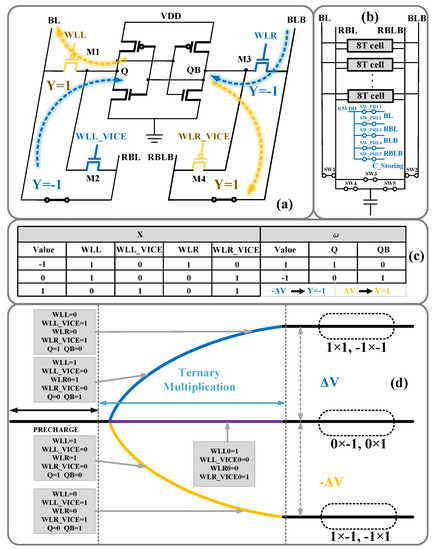
Figure 1.
(a) Configuration of ternary multiplication; (b) 8T cell column; (c) Word lines and Q/QB setting; (d) Waves of bitline (BL)/RBL and BLB/RBLB.
2.1. Ternary Multiplication
When the proposed 8T cell is configured for ternary multiplication, BL and RBL are connected and BLB and RBLB are connected, as shown in Figure 1b. Ternary multiplication can be regarded as X × ω. As shown in Figure 1c, X is presented through the values of the four-word lines, and ω is stored in the storage nodes Q and QB.
Considering X = −1 as an example, all bitline voltages are precharged to 0.5VDD, the WLL_VICE and WLR_VICE are low, and WLL and WLR are high. If ω = −1, i.e., Q = 0, BLB and RBLB charge through M4. If ω = 1, i.e., Q = 1, BLB and RBLB discharge through M3. The voltage curves of BL and RBL and BLB and RBLB are shown in Figure 1d. The accumulation of each multiplication in the same column is presented in the voltage of BLB and RBLB. If X = 1, WLL_VICE and WLR_VICE are high, and WLL and WLR are low. If ω = −1, i.e., Q = 0, the RBL and BL discharge through M2. If ω = 1, i.e., Q = 1, the RBL and BL charge through M1. The 0.5VDD is supplied by voltage buffer. The number of rows is set to 32 in this study.
To explain the calculation process in detail, we considered the following examples: X = −1, ω = −1; X = 1, ω = −1; X = 0. The process mainly consists of the following two steps.
Step 1 As shown in Figure 1b and Figure 2, the bitlines BL, RBL, BLB, and RBLB are connected to storing capacitor C through SW1~5 to store the results of the sum of ternary multiplication, i.e., ∑ (X × ω), in one column. Then, the lines and storing capacitor are precharged to 0.5VDD, and Q = 0 and QB = 1 representing ω = −1 has been written.
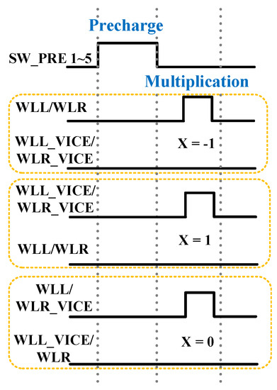
Figure 2.
Setting of ternary multiplication.
Step 2 When X = −1, the M3 and M4 are on for Δt, the M1 and M2 are off, and QB is connected to BLB and RBLB. The voltage of QB is VDD; thus, the BLB and RBLB are charged and raise ΔV through M4, and the ΔV charging corresponds to “+1”. When X = 1, the M1 and M2 are on for Δt, the M3 and M4 are off, and Q is connected to BL and RBL. Since the voltage of Q is 0, the BL and RBL are discharged and decrease ΔV through M2, and the ΔV discharging corresponds to “−1”. If X = 0, the M1–4 is off. Thus, there is no charging or discharging in this case (”+0”).
The output of ternary multiplication operation can be used to form classifiers. Relatively high linearity and a fixed zero value point are necessary for the judgment of classifier. Charging and discharging in different paths can contribute to meeting these requirements without the need for an extra reference voltage generation column.
2.2. Unsigned Multibit Multiplication
Figure 3 shows the configuration and waveforms of the proposed 8T cell array. M1 and M3 are closed. WLL_VICE and WLR_VICE represent the multiplicand and the QB nodestores the multiplier. M2 and M4 are used as the discharge and charge paths, respectively. Assuming that the multiplier and multiplicand are X1 and X2, respectively, their range is between 0 and 8. Furthermore, X1 is stored in four adjacent QB nodes in the same row, and X2 is reflected in the enabled times of WLL_VICE and WLR_VICE. After RBL and RBLB are precharged and predischarged to VDD and VSS, respectively, WLL_VICE and WLR_VICE are enabled; enabling WLL_VICE and WLR_VICE asynchronously enhances stability. If the binary bit stored in QB is 1, the RBL and RBLB will discharge and charge through M2 and M4, respectively. Therefore, the voltage difference of the LSB is enlarged as compared with the existing discharge methods [4,11].
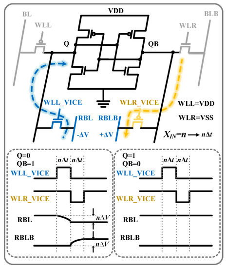
Figure 3.
Configuration and waveforms of the proposed 8T cell in unsigned multibit multiplication.
Figure 3 and Figure 4 show the adder module of unsigned multibit multiplication. Unlike existing works [21], only capacitors with the same size are required to realize different weights, as shown in Figure 4. Because the proposed charge sharing method does not require capacitors of different values to form different weights, the area cost is significantly reduced.
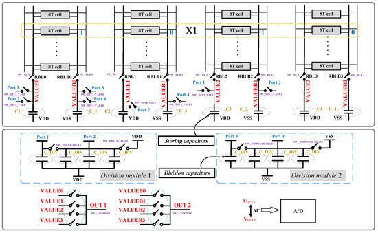
Figure 4.
Unsigned multibit multiplication and charge sharing division modules.
Multipliers that exist in multiple rows can be operated and accumulated simultaneously. For simplicity, the following is an example of one row operation. Considering X1 = 5 and X2 = 3 as an example, the binary bits of X1 are 0101, and therefore QB3–QB0 is 0101. The enabled times of WLL_VICE and WLR_VICE are 3Δt. The multiplication consists of the. following six steps:
STEP 1 RBL and RBLB are precharged and predischarged to VDD and VSS, respectively. In addition, the storing capacitors C0~C3 responding to RBL0~3 are precharged to VDD and the storing capacitors C0~C3 responding to RBLB0~3 are predischarged to VSS. All C_DIVs in division modules 1 and 2 in Figure 4b that realize different weights are precharged to VDD and VSS to perform the next steps.
STEP2 As shown in Figure 3, WLL_VICE and WLR_VICE are enabled for 3Δt, representing X2 = 3. Therefore, RBL2 and RBL0 discharge 3ΔV, and RBLB2 and RBLB0 charge 3ΔV. The storing capacitors, C0~C3 and C_0~C_3, are connected to RBL3~0 and RBLB3~0 to store the discharged and charged voltages, respectively.
STEP3 As shown in Figure 4, the storage capacitors C0~C3 and C_0~C_3 are disconnected from RBL and RBLB, respectively. The voltages of the storing capacitors are labeled as VALUE0~3 and VALUEB0~3. VALUE0 shares the charge with three capacitors in division module 1 (DIV 1) through Port 2 to realize the operation of division 4, and VALUE2 shares the charge with one capacitor in DIV 1 through Port 1 to realize the operation of division 2. Therefore, the voltage level of VALUE0 changes to VDD − 3/4ΔV, and that of VALUE2 changes to VDD − 3/2ΔV. The connections between the RBLB and DIV 2 are similar, and therefore the voltage levels of VALUEB0 and VALUEB2 are VSS + 3/4ΔV and VSS + 3/2ΔV, respectively.
STEP4 The capacitors C_DIV in DIV 1 and DIV 2 are disconnected from storage capacitors C0~C3 and C_0~C_3; then, the capacitors C_DIV in DIV 1 and DIV 2 are precharged and predischarged again.
STEP5 After the capacitors in DIV 1 and DIV 2 are precharged and predischarged again, VALUE0 shares the charge with one capacitor in DIV 1 through Port 1 to realize the operation of division 2. Furthermore, VALUE1 shares the charge with three capacitors in DIV 1 through Port 2 to realize the operation of division 4; the changes in VALUEB are similar. Therefore, the voltage levels of VALUE3~0 for VDD, VDD − 3/2ΔV, VDD, VDD − 3/8ΔV, and VALUEB3~0 are VSS, VSS + 3/2ΔV, VSS, and VSS − 3/8ΔV, respectively.
STEP6 VALUE3~0 emerge to form OUT1, and VALUEB3~0 emerge to form OUT2. The OUT1 voltage is VDD − 15/32ΔV, and the OUT2 voltage is VSS + 15/32ΔV. The voltage difference is doubled as compared with existing works [4,11]. The voltages of the storage capacitors are shown in Figure 5.
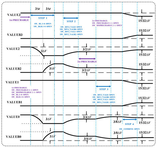
Figure 5.
Unsigned multibit multiplication bitline wave.
2.3. SRAM Read/Write Operation and Logic Operation
Figure 6 shows the configuration of the SRAM read/write operation and the logic operation (Figure 6a). The read/write operation method is similar to that for the 6T cell. As shown in Figure 6b,c, the proposed structure can realize different logic operations in a single cycle. The RBL and RBLB are configured as two outputs, and BL is connected to BLB, which is used as the third output.
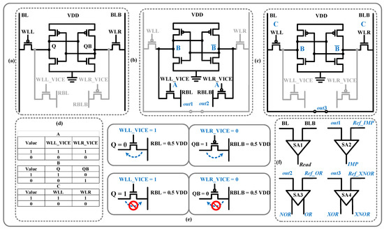
Figure 6.
(a) Read/write configuration; (b) IMP and NOR/OR configuration; (c) XOR/XNOR configuration; (d) Operation element setting; (e) NMOS/PMOS discharge/charge with 0.5VDD precharge voltage; (f) The SA setting of logic.
The voltage of the RBL is determined by WLL_VICE and the storage node and the voltage of the RBLB is determined by WLR_VICE and the storage node; these values are used to realize the IMP and OR operation. The voltage of BL and BLB is determined by separated WLs—WLL and WLR, which realize XOR and XNOR operations. Figure 6d shows the logic values and their corresponding voltages of WLL_VICE, WLR_VICE, Q, QB, WLL, and WLR.
In the IMP operation, the RBL voltage is precharged to VPRE = 0.5VDD. As shown in Figure 7a, when A = 1, WLL_VICE is high, and when B = 0, then Q = 0, and thus the RBL discharges. The SA2 in Figure 6f outputs “0”. In contrast, if B = 1 and Q = 1 because VWLL_VICE-VPRE is around Vth, the RBL does not charge considerably. The SA2 outputs “1”. When A = 0, WLL_VICE is low, and then RBL holds a precharged voltage regardless of whether B = 0 or B = 1. The SA2 outputs “1”.
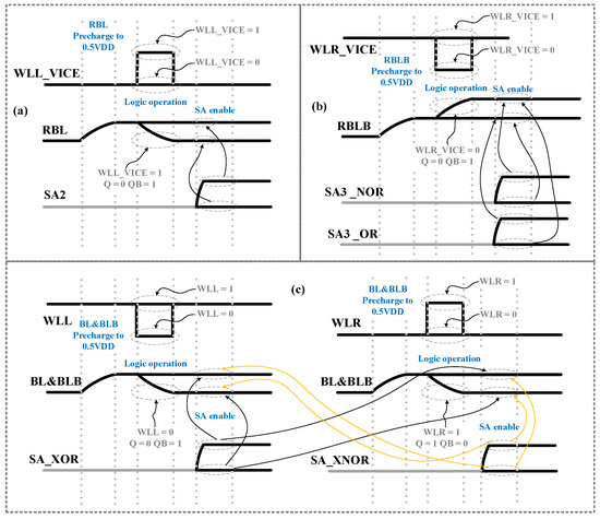
Figure 7.
(a) IMP WLL_VICE and RBL waves; (b) OR WLR_VICE and RBLB waves; (c) XNOR WLL_VICE, WLR_VICE and BL and BLB waves.
In the NOR/OR operation, as shown in Figure 7b, after the RBLB voltage is precharged to VPRE, when A = 1, the WLR_VICE is high; then, the RBLB holds a precharged voltage regardless of whether B = 0 or B = 1. When A = 0, WLR_VICE is low. If B = 0, QB = 1, and RBLB charges. If B = 1, QB = 0 because VPRE-VWLL_VICE is around Vth, and RBLB does not discharge.
In the XOR/XNOR operation, as shown in Figure 7c, after the BL and BLB are precharged to VDD, when C = 0, and WLL and WLR are low. If B = 0, BL discharges, and SA4 outputs “0/1”. If B = 1, BL does not discharge. SA4 outputs “1/0”. When C = 1, WLL and WLR are high. If B = 0, the BLB does not discharge and the SA4 outputs “1/0”. If B = 1, the BLB discharges and the SA4 outputs “0/1”.
All the above-mentioned logic operations can be performed simultaneously in one cycle, because different types of operations adopt different bitlines, and the threshold losses of NMOS and PMOS are utilized to form unidirectional charging and discharging paths, as shown in Figure 6e. The results of different logic operations are obtained in the outputs of SAs, as shown in Figure 6f.
We considered A = 1, B = 0 and A = 0, B = 0 as examples to introduce the process of IMP and OR/NOR. The process mainly consists of the following three steps, as shown in Figure 7a,b:
Step 1 The RBL and RBLB are precharged to 0.5VDD.
Step 2 If A = 1, a high pulse voltage passes through WLL_VICE, and WLR_VICE is always high. If A = 0, WLL_VICE remains low, a low pulse voltage passes through WLR_VICE, and Q = 0 and QB = 1 correspond to B = 0. As shown in Figure 7a,b, when A = 1 and B = 0, RBL discharges, and RBLB remains 0.5VDD. When A = 0 and B = 0, RBL remains 0.5VDD and RBLB charges.
Step 3 SA2 and SA3 are enabled. When A = 1 and B = 0, SA2 outputs “0”, SA3_NOR outputs “0”, and SA3_OR outputs “1”. When A = 0 and B = 0, SA2 outputs “1”, SA3_NOR outputs “1”, and SA3_OR outputs “0”.
We considered B = 1, C = 1 and B = 1, C = 0 as examples to introduce the process of XNOR/NOR. The process mainly consists of the following three steps, as shown in Figure 7c:
Step 1 The BL and BLB are connected and precharged to VDD.
Step 2 If C = 1, WLL remains high and a high pulse voltage passes WLR. If C = 0, a low pulse voltage passes through WLL and WLR remains low. As shown in Figure 7c, if B = 1 and C = 1, BL and BLB discharge through M3. If B = 1 and C = 0, although M1 is on, BL and BLB remain high to a high Q value.
Step 3 The SA4 is enabled. If B = 1 and C = 1, SA4_XOR outputs “0”, and SA4_XNOR outputs “1”. If B = 1 and C = 0, SA4_XOR outputs “1”, and SA4_XNOR outputs “0”.
3. Simulation Results
We built the circuit level simulation model of the CIM array in the Cadence environment. However, the control signals are generated by the pulse generator (vpwl). In the simulation environment, Cadence Spectre, we have set the initial conditions, such as bitline initial voltage. Before the simulation, the values involved in the operation have been stored in the array or transferred to the pulse width of the word line. Different operation processes use corresponding operation sequences. Table 1 shows the simulation setting. Other environment settings follow the default of Cadence Spectre. To analyze the simulation results, we simulate the whole proposed circuit and measure the output signal line voltage. The operation time is calculated by the Cadence calculation function. The total operation current is measured on the power supply. The control and result waves of unsigned multibit multiplication are shown in Figure 8 as an example.

Table 1.
Setting of simulation.
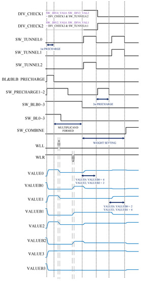
Figure 8.
Control and result waves of the unsigned multibit multiplication.
Table 1 shows the simulation setting. The power consumption and frequency test methods are implemented as follows: Four columns in the 32 × 32 array are enabled, and the additional circuits for the four columns used for the specified functions are activated in the specified operation, respectively. The 28 other columns and additional circuits are not activated. However, the additional circuits of these columns are powered, and their static power consumption is included into total power consumption in each operation. The operation time starts from the precharge and ends at the time when the operation result provides a stable output; subsequently, the frequency is calculated. The total power consumption in this interval is divided by all the bits involved in the operation to get the energy/bit.
The bitline voltages of the ternary multiplication–addition, their theoretical values, and error distribution are shown in Figure 9a. When the theoretical value OUTvalue equals 0, Vout is in the middle point, because the range of discharging and charging is balanced. The maximum error of the ternary multiplication–addition is only 1. The output values of the unsigned multibit multiplication (OUT-VALUE), the corresponding theoretical values (Theory-VALUE), and the error distribution are shown in Figure 9b. The maximum error of the unsigned multibit multiplication is only 3, the linearity and the error can meet the requirement of the machine learning algorithms [4,6,10,21]. The minimum multiplication value is 0, and the maximum multiplication value is 64. The energy and frequency in the logic operation at different supply voltages are shown in Figure 9c,d, respectively.
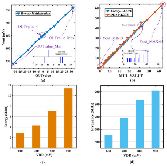
Figure 9.
(a) Theoretical values of ternary multiplication–addition vs. bitline voltages and error distribution; (b) Theory values of unsigned multibit multiplication vs. out-value and error distribution; (c) Energy of logic operation; (d) Frequency of logic operation.
The proposed structure is compared with other reported works, and the results are summarized in Table 2. In this study, the energies of the ternary multiplication, unsigned multibit multiplication, and logic operations are 1.273, 411.75, and 11.375 fJ/bit, respectively. The frequencies for the ternary multiplication, unsigned multibit multiplication, and logic operation are 526, 154, and 909 MHz, respectively. All logic operations can be realized in one cycle simultaneously, therefore, the proposed structure exhibits lower energy consumption.
Table 2.
Comparisons with other reported works.
Table 3 shows the static noise margin (SNM) of proposed 8T cell and 6T cell. The proposed 8T cell have the same read SNM (RSNM) with 6T. Although the write SNM (WSNM) of the proposed 8T cell is lower than 6T cell, more functions can be realized in the proposed 8T cell.
Table 3.
Comparison of SNM.
Due to the logic and ternary multiplication should be achieved on 0.5VDD bitline voltage, we evaluated the Pseudo-read SNM. In the logic operation, only one of M2 and M4 is on when the 0.5VDD bitline is used, so we tested the noise margin in four different cases. In Case 1, M2 is on, and noise signal is added on QB node. In Case 2, M2 is on, and noise signal is added on Q node. In Case 3, M4 is on, and noise signal is added on Q node. In Case 4, M4 is on, and noise signal is added on QB node. In ternary multiplication operation, we tested the noise margin with a similar method. The results are shown in Table 4.
Table 4.
Pseudo-read static noise margin (SNM).
4. Conclusions
In this work, an 8T cell array that can be configured in the ternary multiplication, unsigned multibit multiplication, and logic operation modes, was proposed. The following are achieved using the 8T cell array: (1) Ternary multiplication is realized without the need for reference voltage generation array. (2) The voltage difference of the unsigned multibit multiplication operation is enlarged. (3) Different logic operations are achieved in a single cycle.
The logic operation energy is 11.375 fJ/bit at 900 mV, and the frequency is 909 MHz. Because the IMP logic is implemented, all types of logic operations can be generated via the combination of IMP logic.
Author Contributions
Conceptualization, J.Z. and Z.L.; validation, J.Z and W.L.; data curation, J.Z. and Q.Z.; Writing—original draft preparation, J.Z. and W.L.; Writing—review and editing J.Z. and Z.L.; supervision, Z.L., and X.W.; project administration, J.C.; funding acquisition, X.W. and C.P. All authors have read and agreed to the published version of the manuscript.
Funding
This work was funded by the National Key R&D Program of China, grant number 2018YFB2202602, the State Key Program of the National Natural Science Foundation of China, grant number 61934005, the National Natural Science Foundation of China under grant 62074001, and the National Science and Technology Major Project, grant number 2017ZX01028-101-00.
Data Availability Statement
The data used to support the findings of this study are available from the corresponding author upon request.
Conflicts of Interest
The authors declare no conflict of interest.
References
- Biswas, A.; Chandrakasan, A.P. CONV-SRAM: An Energy-Efficient SRAM with In-Memory Dot-Product Computation for Low-Power Convolutional Neural Networks. IEEE J. Solid-State Circuits 2019, 54, 217–230. [Google Scholar] [CrossRef]
- Hanchun, C.; Jinfu, L.; Chunlung, H.; Chitien, S. Configurable 8T SRAM for Enbling in-Memory Computing. In Proceedings of the 2nd International Conference on Communication Engineering and Technology (ICCET), Nagoya, Japan, 12–15 April 2019; pp. 139–142. [Google Scholar]
- Khwa, W.S.; Chen, J.J.; Li, J.F.; Si, X.; Yang, E.Y.; Sun, X.; Liu, R.; Chen, P.-Y.; Li, Q.; Yu, S.; et al. A 65 nm 4 Kb algorithm-dependent computing-in-memory SRAM unit-macro with 2.3 ns and 55.8 TOPS/W fully parallel product-sum operation for binary DNN edge processors. In Proceedings of the 2018 International Solid-State Circuits Conference (ISSCC), San Francisco, CA, USA, 11–15 February 2018; pp. 496–498. [Google Scholar]
- Shihui, Y.; Zhewei, J.; Jaesun, S.; Mingoo, S. XNOR-SRAM: In-Memory Computing SRAM Macro for Binary/Ternary Deep Neural Networks. IEEE J. Solid-State Circuits 2020, 55, 1733–1743. [Google Scholar]
- Xiaoyu, S.; Rui, L.; Xiaochen, P.; Shimeng, Y. Computing-in-Memory with SRAM and RRAM for Binary Neural Networks. In Proceedings of the 14th IEEE International Conference on Solid-State and Integrated Circuit Technology (ICSICT), Qingdao, China, 31 October–3 November 2018; pp. 1–4. [Google Scholar]
- Agrawal, A.; Jaiswal, A.; Roy, D.; Han, B.; Srinivasan, G.; Ankit, A.; Roy, K. Xcel-RAM: Accelerating Binary Neural Networks in High-Throughput SRAM Compute Arrays. IEEE Trans. Circuits Syst. I Regul. Pap. 2019, 66, 3064–3076. [Google Scholar] [CrossRef]
- Qing, D.; Supreet, J.; Mehdi, S.; Yejoong, K.; Sylvester, D. A 0.3V VDDmin 4+2T SRAM for searching and in-memory computing using 55 nm DDC technology. In Proceedings of the 2017 Symposium on VLSI Circuits, Kyoto, Japan, 12–15 June 2017; pp. C160–C161. [Google Scholar]
- Jeloka, S.; Akesh, N.B.; Sylvester, D.; Blaauw, D. A 28 nm Configurable Memory (TCAM/BCAM/SRAM) Using Push-Rule 6T Bit Cell Enabling Logic-in-Memory. IEEE J. Solid-State Circuits 2016, 51, 1009–1021. [Google Scholar]
- Amogh, A.; Akhilesh, J.; Chankyu, L.; Kaushik, R. X-SRAM: Enabling In-Memory Boolean Computations in CMOS Static Random Access Memories. IEEE Trans. Circuits Syst. I Regul. Pap. 2018, 65, 4219–4232. [Google Scholar]
- Mingu, K.; Sujan, K.G.; Ameya, P.; Naresh, R.S. A Multi-Functional In-Memory Inference Processor Using a Standard 6T SRAM Array. IEEE J. Solid-State Circuits 2018, 53, 642–655. [Google Scholar]
- Zhewei, J.; Shihui, Y.; Jaesun, S.; Mingoo, S. C3SRAM: An In-Memory-Computing SRAM Macro Based on Robust Capacitive Coupling Computing Mechanism. IEEE J. Solid-State Circuits 2020, 55, 1888–1897. [Google Scholar]
- Haerang, C.; Yosep, L.; Jaejoon, K.; Sungjoo, Y. A Novel In-DRAM Accelerator Architecture for Binary Neural Network. In Proceedings of the 2020 IEEE Symposium in Low-Power and High-Speed Chips (COOL CHIPS), Kokubunji, Japan, 11–15 February 2018; pp. 494–495. [Google Scholar]
- Mustafa, F.A.; Akhilesh, J.; Kaushik, R. In-Memory Low-Cost Bit-Serial Addition Using Commodity DRAM Technology. IEEE Trans. Circuits Syst. I Regul. Pap. 2020, 67, 155–165. [Google Scholar]
- Yu, C.; Yoo, T.; Kim, H.; Kim, T.T.H.; Chuan, K.C.T.; Kim, B. A Logic-Compatible eDRAM Compute-In-Memory with Embedded ADCs for Processing Neural Networks. IEEE Trans. Circuits Syst. I Regul. Pap. 2020, 67, 155–165. [Google Scholar]
- Chen, W.H.; Li, K.X.; Lin, W.Y.; Hsu, K.H.; Li, P.Y.; Yang, C.H.; Xue, C.X.; Yang, E.Y.; Chen, Y.K.; Chang, Y.S.; et al. A 65 nm 1 Mb Nonvolatile Computing-in-Memory ReRAM Macro with Sub-16ns Multiply-and-Accumulate for Binary DNN AI Edge Processors. In Proceedings of the 2018 International Solid-State Circuits Conference (ISSCC), San Francisco, CA, USA, 15–17 April 2020; pp. 1–3. [Google Scholar]
- Yan, L.; Huaqiang, W.; Weier, W.; Wenqiang, Z. Novel In-Memory Matrix-Matrix Multiplication with Resistive Cross-Point Arrays. In Proceedings of the 2018 IEEE Symposium on VLSI Technology(ISVLSIT), Honolulu, HI, USA, 18–22 June 2018; pp. 31–32. [Google Scholar]
- Yang, Y.; Mathew, J.; Pontarelli, S.; Ottavi, M.; Pradhan, D.K. Complementary Resistive Switch-Based Arithmetic Logic Implementations Using Material Implication. IEEE Trans. Nanotechnol. 2016, 15, 94–108. [Google Scholar] [CrossRef]
- Pan, Y.; Ouyang, P.; Zhao, Y.; Kang, W.; Yin, S.; Zhang, Y.; Zhao, W.; Wei, S. A Multilevel Cell STT-MRAM-Based Computing In-Memory Accelerator for Binary Convolutional Neural Network. IEEE Trans. Magn. 2018, 54, 1–5. [Google Scholar] [CrossRef]
- Zhezhi, H.; Shaahin, A.; Deliang, F. Exploring STT-MRAM based In-Memory Computing Paradigm with Application of Image Edge Extraction. In Proceedings of the 2017 IEEE 35th International Conference on Computer Design(ICCD), Boston, MA, USA, 5–8 November 2017; pp. 439–446. [Google Scholar]
- Hao, Y.; Hebin, R.C.; Ethan, C.A.; Xuehai, Q.; Lide, D. iCELIA: A Full-Stack Framework for STT-MRAM-Based Deep Learning Acceleration. IEEE Trans. Parallel Distrib. Syst. 2020, 31, 408–422. [Google Scholar]
- Qing, D.; Mahmut, E.S.; Burak, E.; Dar, S.; Winsan, K.; Hungjen, L.; Yih, W.; Jonathan, C. A 351 TOPS/W and 372.4 GOPS Compute-in-Memory SRAM Macro in 7 nm FinFET CMOS for Machine-Learning Applications. In Proceedings of the 2020 IEEE International Solid-State Circuits Conference (ISSCC), San Francisco, CA, USA, 16–20 February 2020; pp. 242–244. [Google Scholar]


Publisher’s Note: MDPI stays neutral with regard to jurisdictional claims in published maps and institutional affiliations. |
© 2021 by the authors. Licensee MDPI, Basel, Switzerland. This article is an open access article distributed under the terms and conditions of the Creative Commons Attribution (CC BY) license (http://creativecommons.org/licenses/by/4.0/).