1. Introduction
Vision processing chips have proven to be highly efficient for computer vision tasks by integrating the image sensor and vision processing unit (VPU) together in the recent works [
1,
2,
3]. Most of them utilize a Single-Instruction-Multiple-Data (SIMD) array of processing elements (PE) connected with the sensor directly. Consequently, they can eliminate the pixels transmission bottleneck and execute vision tasks in a parallel way.
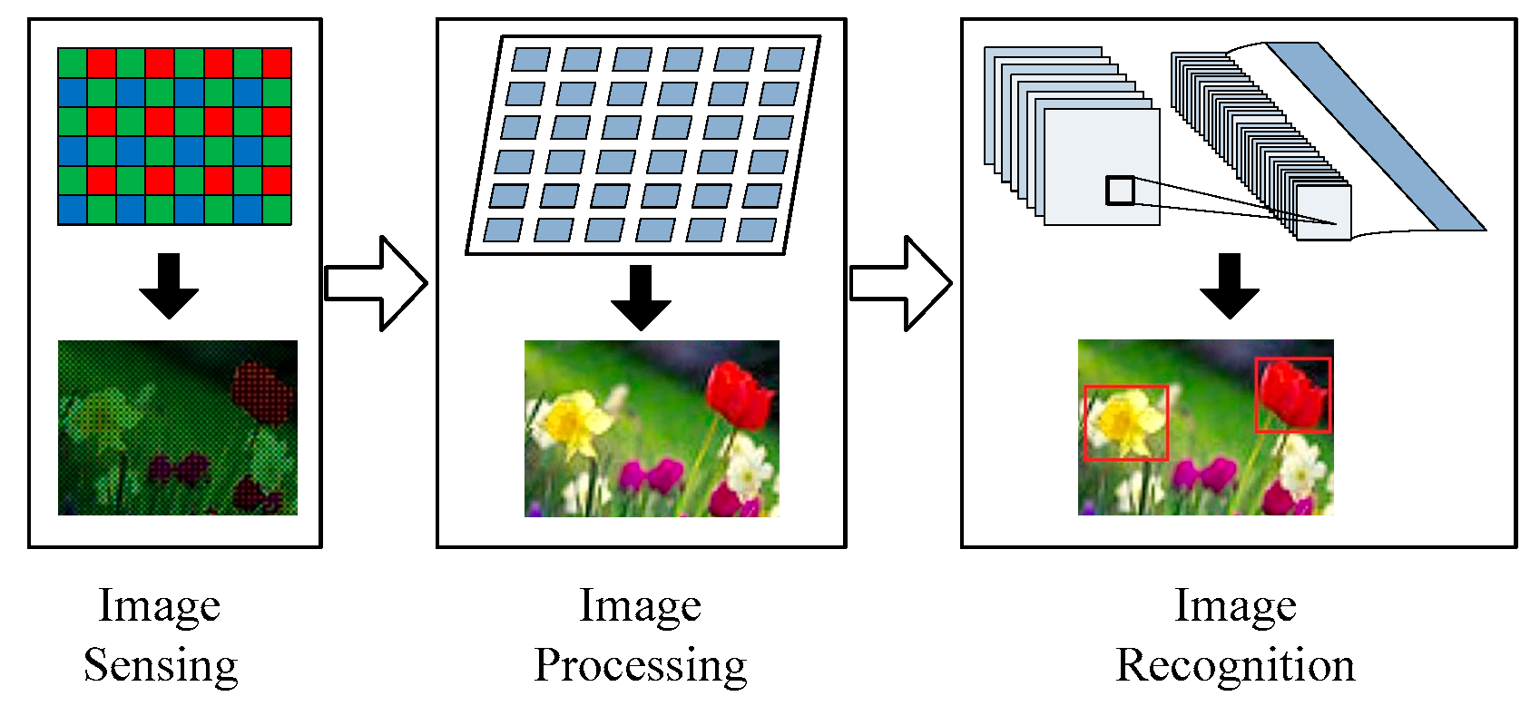
The vision tasks mainly consist of image signal processing (ISP) algorithms and recognition algorithms [
1], as illustrated in
Figure 1. All the algorithms are performed on the PE array in the VPU. On the conventional vision chips, recognition algorithms including Speed-up Robust Features (SURF) [
4], Scale-Invariant Feature Transform (SIFT) [
5] and Features from Accelerated Segment Test (FAST) [
6] are usually applied. Recently, the artificial neural networks have shown great performance on the computer vision tasks [
7,
8,
9,
10]. Therefore, works [
1,
11] proposed the VPUs that try to exploit the conventional PE array for self-organizing map (SOM) neural networks. However, these conventional architectures are not efficient for modern neural networks. They do not contain the multiply accumulators (MAC), which are essential to accelerate the neural network processing [
12,
13,
14]. For instance, the convolutional neural networks (CNNs) are very important tools for vision recognition tasks [
15,
16,
17,
18], and all the conventional VPUs show poor performance on them.
Therefore, many new specific designs have been proposed for high-speed CNNs’ processing in the last few years, called neural network processing units (NPUs) [
19]. Additionally, a lot of effort has been made to shift the NPUs closer to the sensors, such as work [
20,
21,
22,
23,
24] to reduce the expensive pixels transmission. However, those NPUs cannot be connected to the sensors directly, because they cannot process the RAW images provided by the sensors. Some essential ISP tasks, such as demosaicing, need to be executed on the RAW images first to convert them into the proper format. Only after that can the NPUs process them. On the other hand, high-quality pictures are required in many vision systems rather than RAW images, such as the closed-circuit televisions and IP cameras [
23]. NPUs cannot accomplish the ISP tasks efficiently to well tune the RAW images. Therefore, an extra ISP unit is equipped between the NPUs and sensors in those works [
25]. This will consume more power and hardware resources.
We compare the NPUs with the ISP units. There are two major differences between them. The first one is the different hardware modules. Similar to the conventional VPUs, the primary computing modules in the ISP units are the arithmetic logic units (ALU) with simple functions, including addition, subtraction and logical operations [
1,
2,
11,
26,
27]. In contrast, the NPU must integrate a lot of MACs in it to accelerate the convolution computation [
28,
29,
30]. Each PE in the ISP unit contains a small memory to access the data locally [
31], while the MACs in the NPU usually obtain data from the large global buffers [
32]. The second difference is in the architectures. As illustrated in works [
1,
7], the ISP units are a von Neumann type, while the NPUs adopt the non-von Neumann architecture.
However, we also find that the NPUs and the ISP units have some shared requirements for hardware resources, such as the memory and buses. Additionally, ALUs can also execute the non-convolutional tasks in the CNNs, such as pooling, activating, quantization and addition for a shortcut. On the other hand, the two architectures have different instructions and data flows; therefore, they can run independently, even though they are implemented on the same hardware resources. Moreover, the 2D SIMD framework is widely used in both the NPUs and the ISP units. Therefore, integrating the NPU and the ISP unit into one VPU is practicable. Additionally, a vision task can be executed on it in a pipelined way. It will be highly efficient, with shared hardware resources and parallel operations.
We have noticed that the MAC utilization determines the efficiency of the NPU in the vision tasks. The NPU should maintain a high MAC utilization for all the layers of CNNs with varied strides and kernel sizes. Furthermore, since the vision chip is a power-sensitive embedded system, the lightweight CNNs with various irregular operations will be widely used on it. Therefore, the NPU in the vision chip should be highly flexible to process the lightweight CNNs without a significant loss in the MAC utilization. Work [
33] proposed a CNN accelerator with a MAC utilization of 98% for convolutional layers, but it did not support the full-connection (FC) layers. On the contrary, work [
34] is only optimized for FC layers. Many NPUs, such as works [
7,
33,
35], are specifically designed for the convolution with a 3 × 3 kernel, and a lot of MACs will be idle when processing a convolution with other kernel sizes. Additionally, most works have not considered the lightweight CNNs. They are not efficient for some irregular operations, such as Squeeze and Excitation or depth-wise convolution. For example, the NPU in work [
36] shows a high performance for VGG16 but suffers a loss of more than 50% in the MAC utilization for mobilenetV1 and V2. The same problems exist in the works [
37,
38]. Although work [
39] is designed with the consideration of lightweight CNNs, it does not show a high MAC utilization compared with the other works.
In this paper, we proposed a novel pipelined hybrid VPU architecture that integrates the NPU and the ISP unit in a 2D SIMD PE array. Each PE contains four MACs and one ALU, and a small local memory is connected to both the MACs and the ALU. Furthermore, the NPU we designed naturally supports all kind of strides and kernel sizes, and the ALUs can process the non-convolutional tasks. By adding a 1D Row processor, this NPU can execute the FC and convolutional operations simultaneously.
The hybrid VPU is designed to process the image flow, and the ISP and CNN tasks are executed for each frame sequentially. Moreover, the CNNs usually consist of several consecutive subtasks such as convolution, pooling, activating and FC computation. Therefore, a vision task can be regarded as a set of serial subtasks. The convolution and FC computation are processed on the PE array and Row processor, respectively. The ISP, pooling and activating subtasks will share the ALUs. The on-chip buffers and buses are shared for all the subtasks. Based on the above factors, this paper proposed the pipeline strategies with the time-shared hardware resources. The ISP of one frame can be executed simultaneously with the CNN processing of another frame, and the subtasks in the CNN for different layers and frames are also pipelined. The schedules to time-share the hardware resources are applied in the pipeline strategies. By this means, the VPU can achieve a high utilization of hardware resources and speed-up the vision tasks efficiently. Moreover, with the local memories embedded in each PE and the buses connecting the adjacent MACs, the VPU can load the data into the PE array along with the computation during the CNN processing.
The main innovative characters of this VPU are listed as follows:
We integrate an NPU and an ISP unit into a VPU with shared hardware resources, and a pipeline strategy is designed based on it to seamlessly execute the vision tasks consisting of the ISP and the CNN processing;
A strategy to map the various CNNs onto this VPU is proposed, including the methods to execute irregular operations. A pipelined computing flow for the CNN processing is used to process different layers on the PE array and the Row processor concurrently. It can make full use of the MACs;
A new memory architecture with two groups of buses for MACs is designed. Additionally, based on this, a data flow is proposed to pipeline the data loading and the processing of different layers.
The rest of the paper is organized as follows.
Section 2 presents the preliminary of this work.
Section 3 introduces the architecture of the proposed VPU, and the workflow based on it is detailed in
Section 4.
Section 5 describes the experiments and discusses the results. Finally,
Section 6 concludes this paper.
2. Preliminary
Modern vision tasks have been focused on computer vision in recent years. Additionally, image recognition plays an important role in those tasks. In conventional vision chips [
27,
31], feature extraction algorithms including SURF, FAST and SIFT are used. Since 2012, a lot of neural networks have been proposed and have shown a great performance for computer vision tasks, among which, the CNNs are the most widely used ones. The CNN can be used for image recognition directly or extracting the feature vectors for other applications such as recurrent neural networks (RNN). Additionally, the CNNs can be used as the backbone of object detection networks such as You Only Look Once (Yolo) [
40] and Single Shot MultiBox Detector (SSD) [
41]. Generally speaking, the CNNs are indispensable in the modern vision tasks. Therefore, modern VPUs should be able to process the CNNs efficiently and integrating an NPU is the way to achieve this goal.
Additionally, the ISP units are still essential in the vision tasks to tune the RAW images. Although the CNNs can be used to improve the quality of the images, such as CNN-based denoising, it is uneconomic to perform this in the vision tasks. The image recognition is the main task in vision processing, and it should be processed with the CNN prior to the others. Since this task can consume millions of cycles, the NPU will be kept busy with it. Additionally, stopping the image recognition task for CNN-based denoising will significantly increase the latency of processing an image. Therefore, the ISP units should also be integrated in the VPU.
Meanwhile, the CNNs tasks are far more complicated than the ISP algorithms. with the same computing resources, it can take millions of cycles to accomplish a CNN task, while an ISP task may only cost hundreds of cycles. To deal with this imbalance, more resources should be distributed to the NPU. Moreover, in our design, the ALUs in the ISP units will be also used for the NPU. By this means, the VPU can achieve a high utilization for all hardware resources.
Since the NPU is dominant in the VPU, its resources utilization will determine the efficiency of the VPU. Additionally, the NPU should be flexible for all kinds of CNNs. The layers of CNNs can be divided into two classes based on the dominant hardware requirements to process them. One class is computation-intensive layers (CILs), including the common convolutional layers, group convolution layers and point-wise convolutional layers. The other one is memory-intensive layers (MILs), which are mainly the full-connection (FC) layers in the CNN. The former class needs an enormous amount of computation with high data reusability, while the latter one consumes much higher throughput with barely shared data. Depth-wise convolutional layers are regarded as special CILs with a slightly memory-intensive character. They have both lower data reusability and less computation. Since the hardware requirement varies with the layers, different hardware resources should be distributed to them dynamically in the NPU. For example, more MACs should be used to accelerate the CILs, and more memory bandwidth should be provided for MILs. By exploiting the characteristics of varied layers, we designed two different processing elements clusters efficient for each class. The PE array will be used for the CILs, and the Row processor will process the MILs. The depth-wise convolutional layers can be computed on both clusters. The bandwidth of the external memory is allocated to each cluster on demand, which highly improves the memory utilization.
As mentioned in the previous works, the VPUs can work independently or as the coprocessors. They are designed to be implemented with the sensor on one chip and can be modeled on the FPGA for a performance test. The proposed vision chip in this paper is recommended to work as a coprocessor. It is directly connected to the image sensor and processes the image data with instructions from the host processor. Then, it can send the processing results to the host processor for further tasks. It should be noted that since the VPU is supposed to connect with a fixed sensor, the size of the input images will be constant. Additionally, the size of the PE array should be determined according to the sensor resolution for high utilization. In this paper, the design is implemented with a 7 × 7 PE array, and the sensor resolution is recommended to be an integer multiple of 7 × 7 so that the input pixels can be evenly distributed to the PEs. This will contribute to a high PE utilization. In our experiments, which are discussed in
Section 5, the image sensor is modeled as 224 × 224.
3. The Architecture of the VPU
In this section, the architecture of the proposed VPU will be detailed. The sensor is also an essential component in the vision chip, but it is not the research point of this paper. Therefore, the architecture of the sensor will not be discussed here, but it can be connected with the VPU directly.
3.1. The Overall Architecture
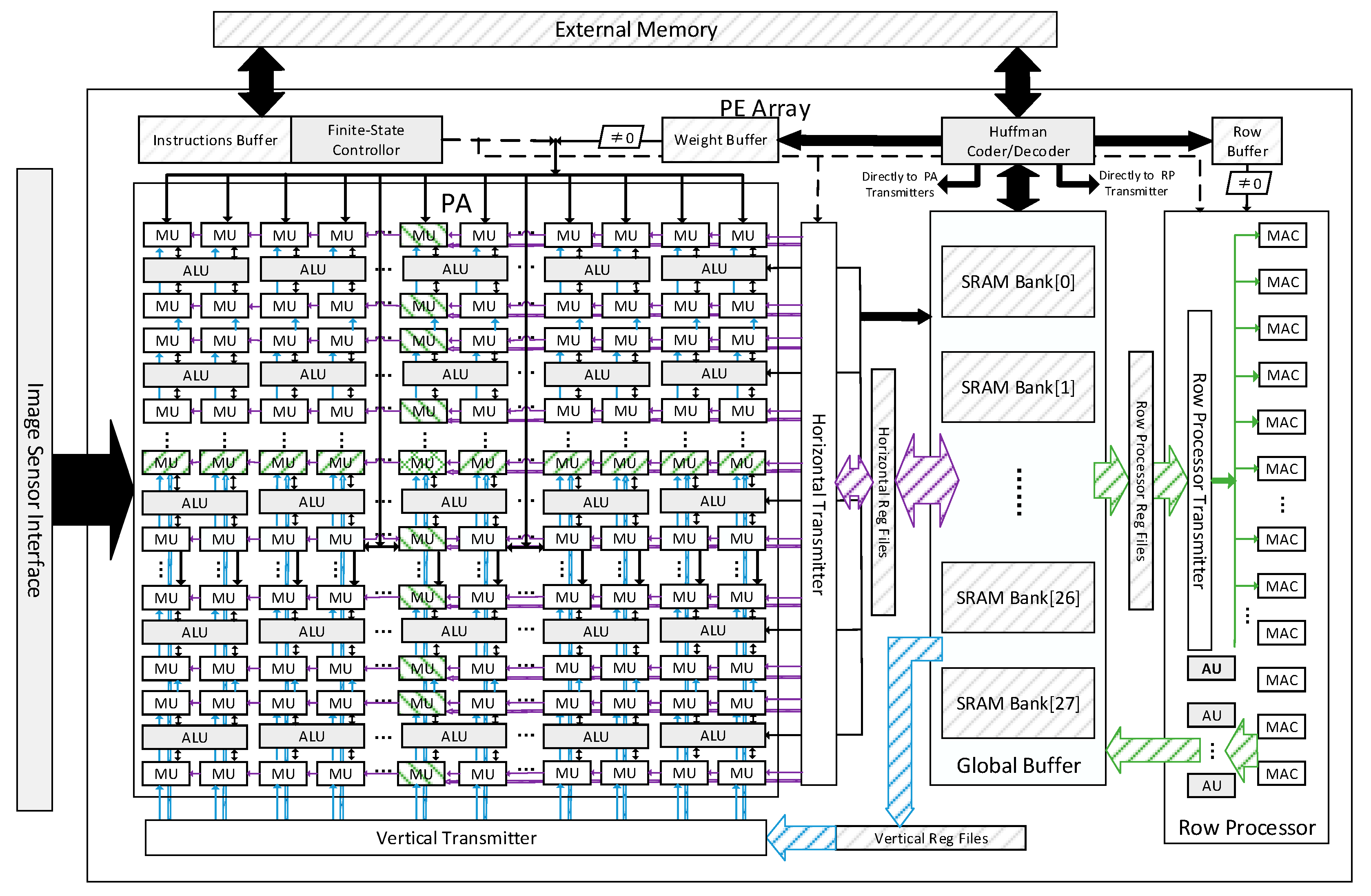
Figure 2 shows the top-level architecture of the proposed vision processor. The main computing core is a 7 × 7 multifunctional PE array and a Row processor with 16 MACs. A global buffer is equipped to provide data for both the PE array and Row processor through three register banks, Horizontal Registers Files (HRF), Vertical Registers Files (VRF) and Row processor Register Files (RPRF). The weights for the PE array are stored in the weight buffers, and the Row processor has a row buffer connected to it. The Huffman Coder and Decoder Module manages the data exchange between the external memory and the global buffer, weight buffer or row buffer with Huffman Coding. The instructions will be loaded and cached in the instructions buffer. A Finite-State controller translates the instructions and generates the control signals for each part of the VPU. The image sensor interface connects the VPU and the sensor. It should be noted that the VPU can be integrate with the image sensor in one chip [
1,
11,
27].
3.2. The Processing Elements Array
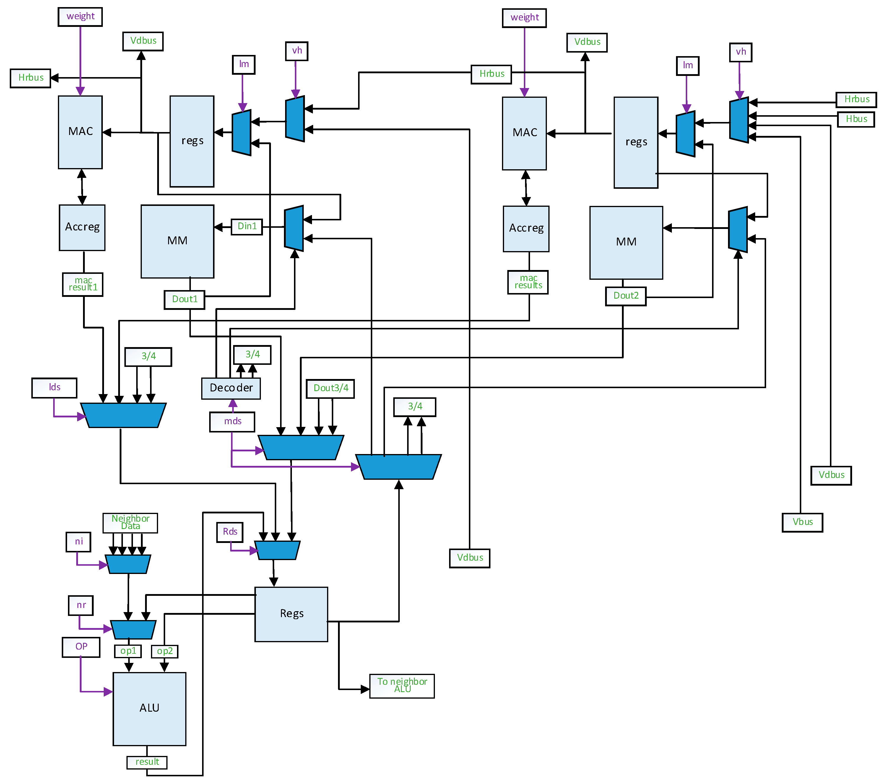
Each PE has four MAC units and one ALU.
Figure 3 shows the architecture of a PE with two MAC units omitted. The PE array can work as a 14 × 14 MAC array and a 7 × 7 ALU array. A group of horizontal buses and a group of vertical buses are used for data transmission in the PE array.
Each MAC unit includes MACs, an accreg for accumulation, several general-purpose registers and one MAC Memory. One of the inputs for MACs is fixed for weights, and the other one obtains activations from the registers. Each MAC unit can transmit data to the upper unit through the VDbus and to the left unit through the HRbus. The 14th column of MAC units can exchange data directly with the HRF through the HRbus, while the seventh column can perform this through the Hbus. The same connections are applied for the 7th and 14th rows of the MAC units and the vertical buses. Those buses enable the PE array to work as four 7 × 7 PE Blocks too. Each PE block can obtain data from the weigh buffer, HRF and VRF independently. PE blocks can efficiently process output fmaps of a small size, especially 7 × 7 fmaps. The same control signals are broadcasted all over the PE array.
The MAC unit can contain more than one MAC. Increasing the quantity of MACs in each unit will raise the computing throughput of the PE array. The MACs in the same units work in the same manner with different data. For brevity, we will describe this work as one MAC in each unit. Correspondingly, the bit-width of the horizontal and vertical buses is the same with the MAC.
The ALU is similar to the neighborhood processors in the work [
2]. Each ALU performs an 8-bit addition, subtraction, logical and shift operations in a single cycle, and can exchange data with the four adjacent ALUs from the left, right, upper or lower PEs. The rightmost column of the ALUs has direct access to the global buffer. Each ALU can exchange data with the MAC memories in the same PE. Inter-ALU data transmission is achieved by column or by row. This enables the ALU array for mid-level ISP algorithms, which requires data from multiple pixels to compute [
2]. The data in the accregs of the MAC units can also be sent to the ALU to execute non-convolutional tasks with different strides.
Generally, the ALUs array is the primary computing module of the ISP unit, while the MAC array and Row processor compose the NPU. All other resources are shared by both the ISP unit and the NPU.
3.3. The Row Processor
The Row processor contains a column of 16 MACs and a column of four activation units. The 16 MACs can, respectively, obtain data from the RPRF or the Huffman Decoder directly. There is no data connection between each MAC. The data from the row buffer will be broadcasted to all the 16 MACs simultaneously for MIL processing. The activation unit contains a sigmoid unit besides the ALU. Each activation unit is connected with four MACs. They obtain data from the MACs and process them. Additionally, the results will be stored into the global buffer by the activation units.
3.4. The Architecture of the On-Chip Memory
The global buffer is the main data memory on the chip. It consists of 28 dual-port SRAM Banks. Those banks can be divided into several groups. Each group can be used as an input or output buffer for the PE array or the Row processor, respectively. Since the input data for CILs are highly reused, they have the priority to be stored in the global buffer.
Registers files HRF, VRF and RPRF are used for data reusing in the convolution computing introduced in
Section 4. The HRF and VRF can also buffer the input during the data loading for the PE array. There are three transmitters between the processors and the register files, as shown in
Figure 2. Those transmitters will align the input data as required.
The weight buffer and the row buffer store the shared data for the PE array and the Row processor, respectively. The weight buffer consists of four SRAM banks. Each bank can provide weights for the entire PE array or be fixed to a PE block. They also work in the double buffering way.
4. The Workflow of the VPU
In this section, we will describe the workflow of the proposed vision processor. The top level of the workflow is summarized as follows:
The sensor captures the RAW image data and transfers them to the ALU array;
The ALU array carries out the ISP tasks and stores the results to the global buffer as input activations for the CNN processing;
The CNN processing tasks are then executed on the PE array and Row processor and generate the final results of the vision processing.
4.1. The Work Flow of the ISP
When instructed to accomplish the ISP tasks, the ALU array works in the traditional way as proposed in the previous works.
The resolution of the sensor is fixed as 224 × 224 RAW-RGB, and it sends an image to the VPU column by column. The image sensor interface will divide a column of pixels into several slices and transmit them to the leftmost column of PEs in the PE array. The pixels can be stored in the MAC memories or transmitted to the rest columns in the PE array by the ALUs. The length of the slice is variable and determined by the algorithms. The smallest length is 14 and each MAC memory will store one pixel, which forms a 14 × 14 patch. For mid-level algorithms, a bigger length will be used.
After a patch of pixels is loaded into the PE array for ISP, the ALU will execute the algorithms. Pixels can be transmitted to the four adjacent PEs and keep going to the farther ones. When the algorithms are accomplished, the results can be stored in the MAC memories for CNN processing or transferred to the global buffer. The pixels can also be loaded back to the PE array from the global buffer for further ISP tasks.
4.2. The Strategy to Map the CNN on the VPU
As mentioned above, the CIL needs more computation resources while more data throughput is required in the MIL. Therefore, we map the CIL on the PE array while the Row processor executes the MIL. The input data for CIL will mainly be stored in the MAC memories. The Row processor will consume most of the bandwidth of the global buffer. The depth-wise convolutional layers can be processed efficiently on both the PE array and the Row processor.
4.2.1. The Mapping Strategy for the Computation-Intensive Layers
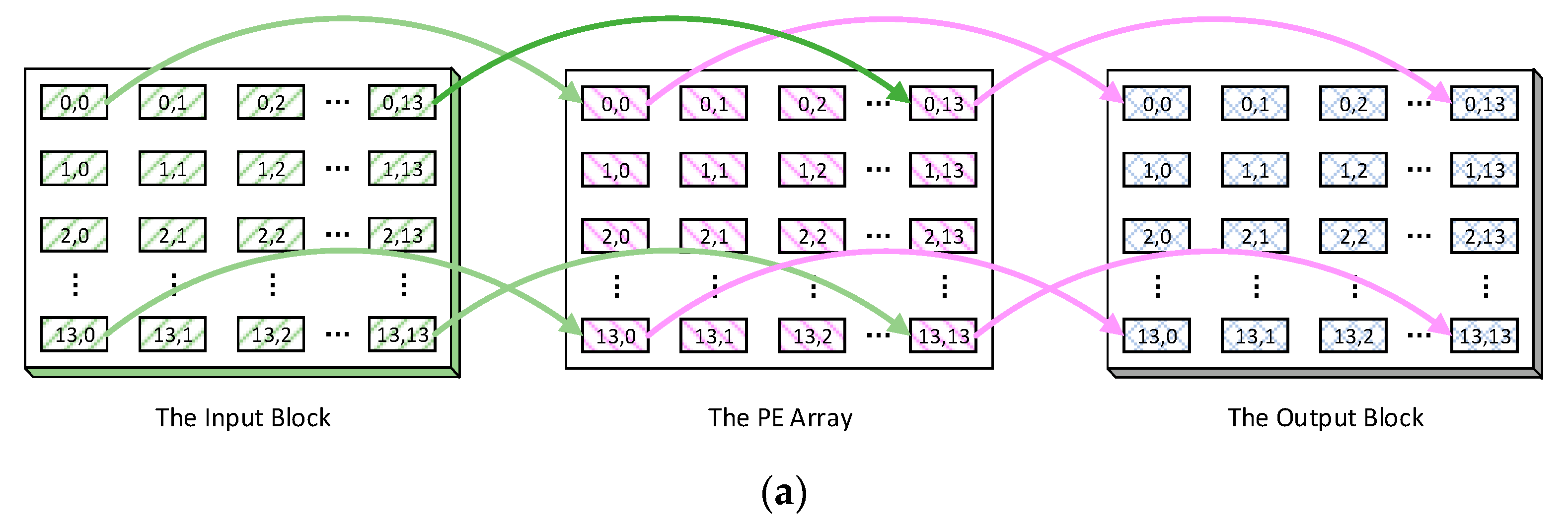
The computation-intensive layers in CNN contain a large number of MAC operations. Input activations are reused to compute every output fmap. Additionally, each output fmap has an exclusive filter shared by all the output pixels in it.
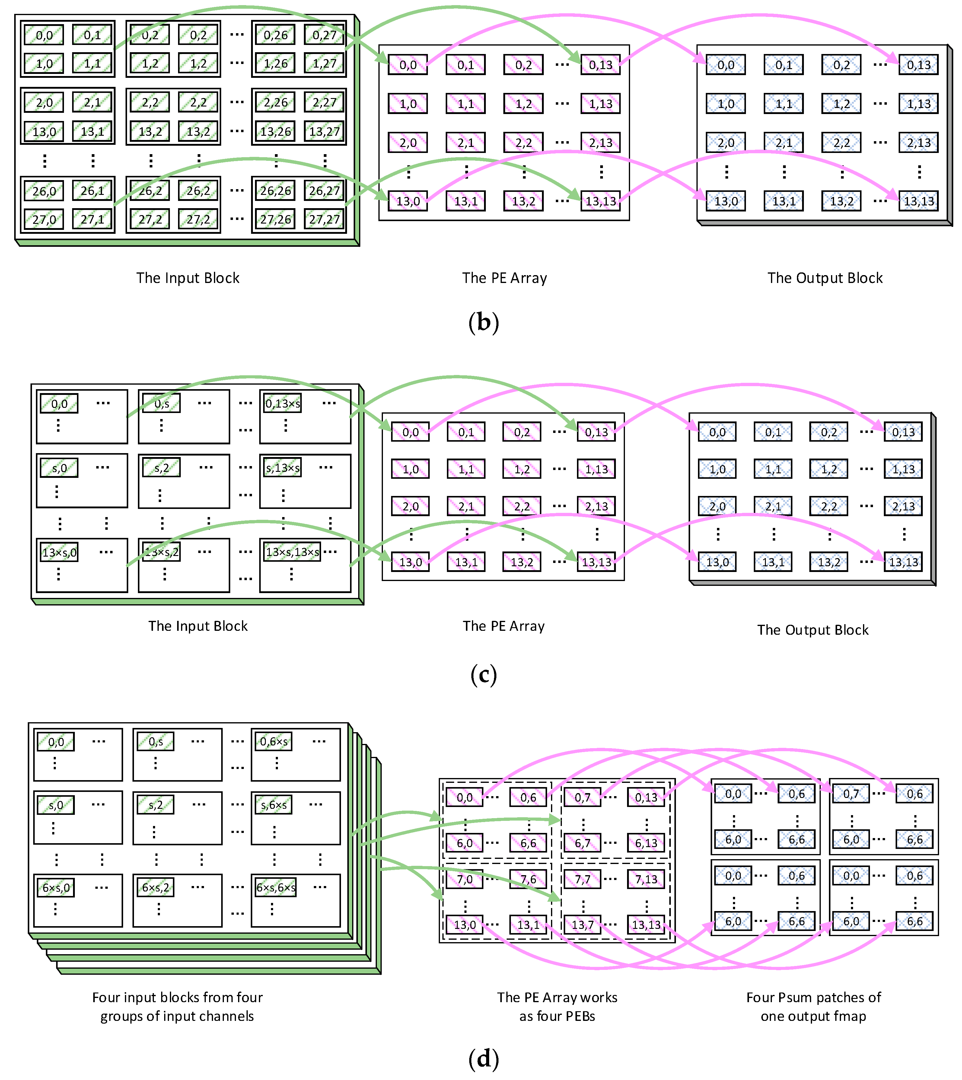
The mapping strategy is output stationary. Firstly, the output fmaps with the size equal to or larger than 14 × 14 are considered, such as 14 × 14, 28 × 28, as illustrated in
Figure 4a–c. We divide one output feature map into several patches of 14 × 14 pixels, and the PE array computes all the pixels of one output patch simultaneously. Each pixel is processed by the MAC unit with the same location in a 14 × 14 matrix. For example,
Figure 4a describes the mapping strategy for the first patch of an output fmap, which is computed on i input channels with a kernel of k × k and a stride of one. To compute the pixel at (0,0) in the output patch, the activations at (0,0) in all i input fmaps will be stored in the memory of the MAC unit (0,0). The same scheme is applied to the rest of the pixels in the output patch. Finally, an input block of i × 14 × 14 activations will be stored in the PE array, which means each input fmap is divided into patches of 14 × 14 too. Additionally, based on this input block, the first patches in all the output fmaps can be computed as the first output block. The other input blocks will be loaded and computed in the same way. Each output block is computed on an independent input block.
Figure 4b shows the mapping strategy when the stride is two, and in this case, four adjacent input activations are stored in each MAC memory. The input patch size is 28 × 28 and an input block of i × 28 × 28 activations is stored in the PE array. This procedure can be generalized to any stride. If the convolution stride is s, the input map will be regarded as being composed of many grids with the size s
2. Additionally, the MAC memory stores the grids of activations in all the input maps with the same location as the coordinative output pixel. Finally, an input block of i × (14 × s) × (14 × s) activations is stored, as shown in
Figure 4c.
A shared coordinate weight from the weight buffer is broadcasted to all the MAC units to be multiplied with the activation in every cycle. The activations in each MAC memory can be transmitted to the left unit through the HRbus or to the upper unit through the VDbus to accomplish the 2D convolution. The 14th column of MAC units will obtain those adjacent activations from HRF, with a similar arrangement for the 14th row and VRF. By repeating the 2D convolution i times, 14 × 14 output pixels of one output fmap will be obtained. Then, a patch in the next output fmap can be computed with a different coordinative kernel sequentially.
Secondly, when the size of output fmaps is 7 × 7, the PE array will work as four 7 × 7 PE blocks. i input channels will be divided into four groups, as shown in
Figure 4d. Each group is an input block and stored in one PE block, respectively. Each MAC memory stores s
2 × i/4 input activations and the size of each input patch is i × (7 × s) × (7 × s). A 7 × 7 output fmap is then mapped onto all four PE blocks and computed onto each input block the same as the 14 × 14 output patch. The kernel will also be divided into four groups and stored in four banks of the weight buffer, in accordance with the input channels. Moreover, the seventh column of MAC units will obtain those adjacent activations from HRF through the Hbus, with a similar arrangement for the seventh row and VRF. Therefore, each PE block will generate a patch of 7 × 7 partial sums for the output fmap on one input block. Finally, the four patches of partial sums will be transmitted and added together by the ALUs to generate the integral 7 × 7 output pixels.
The weight buffer will conduct the zero-check on the weights before broadcasting them. If a weight is zero, the weight buffer will send a skip signal instead of the weight. Then, the PE array will skip all the operations with this weight to save energy.
When a patch of output pixels is accomplished in the MAC array, each MAC unit will send the pixel to the ALU connected to it for non-convolutional tasks including activating, pooling, quantization, batch normalization, biasing and adding for a shortcut. Most of these tasks can be finished in a few cycles, while the MAC array continues processing the convolution layers. Since ALUs and MACs work concurrently, non-convolutional tasks execution will be masked by the convolution computation that usually consumes thousands of cycles. By this means, the processing of the non-convolutional tasks will not suspend the convolutional computation.
The depth-wise convolutional layers can also be processed in this manner, regarded as the CIL with only one input fmap.
4.2.2. The Mapping Strategy for the Memory-Intensive Layers
The memory-intensive layers are mapped on the Row processor. Each MAC of the Row processor executes an output pixel. The depth-wise convolutional layers can also be processed on the Row processor, since they consume less computation than CILs.
When processing the depth-wise convolutional layers on the Row processor, the input activations are stored in the global buffer and transmitted to the MACs through RPRF. Each MAC obtains a specific input activation from the RPRF, respectively, and a shared weight is broadcasted to all the MACs from the row buffer in each cycle, as illustrated in
Figure 5. No data transmission exists between the MACs and reusing activations takes place in the RPRF. This mapping strategy works for the depth-wise convolutional layers with varied stride. When an output pixel is generated, it will be sent to the activation units that the MAC is connected to. Subsequent operations, such as activating and pooling, will be accomplished by them.
In the FC layers, the input activations are shared for every output pixel, while there is no reusability in the weights. Therefore, opposite to the depth-wise convolutional operations, the input activations of the FC layers are stored in the row buffer, while the weights are stored in the global buffer. When processing the FC, an activation is broadcasted to all the MACs and each MAC obtains a coordinative weight from the RPRF, as shown in
Figure 5.
The row buffer also has a zero-skipping scheme for the Row processor, such as the weight buffer.
4.2.3. The Irregular Mapping Conditions
When mapping the layer on the PE array, some irregular conditions may arise. This problem causes a significant loss of MAC utilization in the early works. In this paper, the irregular conditions are also considered to make full use of the MACs.
For the output fmaps of a size equal to or bigger than 14 × 14 with a kernel stride of s, a MAC memory needs to store s2 × i input activations. However, this cannot be achieved when s2 × i is greater than the capacity of the MAC memory, which is assumed as m. In this case, the input channels will be divided into ⌈s2 × i/m⌉ groups. Each group will be loaded into the PE array and computed independently to obtain the partial sums for all output pixels. The partial sums will be transferred to the global buffer or external memory similar to the output pixels. Additionally, after all the groups of input channels are computed, the partial sums will be reloaded into the PE array and added by the ALUs to generate the integral output pixels. For the output fmaps 7 × 7 in size, s2 × i/4 input activations need to be stored in each MAC memory. Additionally, if s2 × i/4 is greater than m, the input channels will be divided into ⌈(s2 × i/4)/m⌉ groups and each group will be computed in order, similarly.
These actions may cause extra access to the external memory. However, when the capacity of MAC memory is large enough, such conditions will rarely happen. According to our survey, when the MAC memory is 512 Bytes, it can satisfy the storage requirement for input activations in 81% of the CILs in the tested CNNs.
The Row processor is flexible, with different lengths of the output pixels column. The output map or vectors can be divided into many groups of 16 pixels. There will be only one group that is less than 16. Therefore, the irregular mapping problem in the Row processor is negligible.
Since the sensor resolution is fixed to 224 × 224 in this work, the sizes of the fmaps in most CNNs are supposed to be multiples of 14 × 14. In spite of this, other sizes of fmaps can also be mapped on the PE array, such as 13 × 13, with a loss of only 13.8% in the MAC utilization.
The other irregular operations used in the lightweight CNNs, such as the group convolution, channel shuffle, Squeeze and Excitation and channel concatenation, can also be mapped on this architecture. For example, the channel shuffle can be performed by changing the loading and storing order of the input fmaps. The squeeze and excitation operation contains global average pooling, FC and channel-wise multiplication. The global average pooling can be performed by shifting and adding the results in the ALU array, and one ALU will conduct the final averaging. The channel-wise multiplication can be regarded as a 1 × 1 depth-wise convolution. The channel concatenation can be realized by jumping to the address of the required input fmaps when loading data. Additionally, the shortcut is loading the former layers into the PE array and adding them to the new ones.
4.3. The Computing Flow for the CNN Processing
The CNN processing is executed on both the PE array and the Row processor with different computing flows.
4.3.1. The Computing Flow on the PE Array
When processing a convolutional layer with a kernel of i × k × k and stride of s on the PE array with an input block, the steps listed below will be taken. A small array of four MAC units is taken as a model for brevity, and it can compute four output pixels in a fmap concurrently. (x,y) refer to the data in row x and column y of the fmap. An input block is already stored in the MAC memories.
Step 1: Each MAC obtains activations (0,0), (0,s), (s,0) and (s,s) in the first input fmap from the local MAC memory, respectively, and performs the first convolution computation with a shared weight, as illustrated in
Figure 6a.
Step 2: Each MAC will obtain the activations (0,1), (0,s + 1), (s,1) and (s,s + 1) from local memory when s is greater than one, or from the right MAC unit through the HRbus/Hbus when s is one, as illustrated in
Figure 6b. As mentioned in
Section 3, activations (0,0) to (0,s − 1) are only stored in MAC unit (0,0), and the location of other activations can be deduced by analogy. Consequently, each MAC will obtain the activations (0,s), (0,s × 2), (s,s) and (s,s × 2) from the right MAC unit. The second convolution will be computed here.
Step 3: Repeat step two until each MAC finishes the computation of (0,k − 1), (0,s + k − 1), (s,k − 1) and (s,s + k − 1). Thus far, the first row of the 2D convolution is finished with k cycles.
Step 4: Each MAC obtains the activations (1,0), (1,s), (s + 1,0) and (s + 1,s) from local memory when s is greater than one, or from the lower MAC unit through the VDbus/Vbus when s is one, as illustrated in
Figure 6c. The same as in step two, activations (0,0) to (s − 1,0) are only stored in MAC unit (0,0). Then, begin to compute the second row of convolution.
Step 5: Repeat steps two and three to finish the second row of the 2D convolution.
Step 6: Repeat steps four and five until the kth row of the 2D convolution is finished. Thus far, the 2D convolution on the first input fmap for these four output pixels is accomplished with k × k cycles.
Step 7: Move to the second input fmap in the MAC memories and start from steps one to six. Another k × k cycles are taken to finish the 2D convolution on the second input fmap.
Step 8: Repeat the above steps to the last fmap of the input block, and four output pixels, (0,0), (0,1), (1,0) and (1,1), are generated with k × k × i cycles.
At last, these four output pixels will then be sent to the ALU to execute tasks such as pooling, RELU, quantization and addition for a shortcut. In the meantime, the MACs are repeating the above steps to compute the output pixels at (0,0), (0,1), (1,0) and (1,1) of another fmaps on the same input block with weights from another kernel. This procedure will go on until an entire output block is generated. On the other hand, if more than one input block is stored in the PE array, the MACs can also compute the output pixels, (0,14), (0,15), (1,14), (1,15), in the same fmap on another input block with the same kernel.
When processing the depth-wise convolution, only steps one–six are taken to compute one output fmap, since only a 2D convolution on one input fmap is required.
The above-mentioned computing flow can be generalized to the whole PE array or four PE blocks. This can guarantee the highly efficient usage of the MACs.
4.3.2. The Computing Flow on the Row Processor
The computing flow on the Row processor is relatively simple. The Row processor will compute a column of 16 output pixels simultaneously.
Each depth-wise output fmap will be regarded as a 1D array and divided into several slices of 16 pixels. For the depth-wise convolution with a kernel of k × k, the first MAC in the Row processor will obtain k2 input activations (0,0), (0,1)… (0,k − 1), (1,0)… (1,k − 1)… (k − 1,k − 1) sequentially from RPRF. Similarly, the second MAC will obtain activations (s,0)… (s + k − 1,k − 1). This can be generalized to all of the other MACs in the Row processor. A shared weight from the row buffer is broadcasted to all the MACs in each cycle. The output pixels will be sent to activation units to finish the other necessary tasks.
For the FC layers, each MAC performs the computation of one output pixel. They will sequentially obtain the weights from RPRF or the Huffman Decoder. Additionally, shared input activations are broadcasted to all the MACs in each cycle. The output pixels are also sent to the activation units for other tasks, including the quantization and sigmoid.
4.3.3. The Pipeline Strategy in the CNN Computing Flow
The pipeline strategy is designed in the computing flow to process the different layers simultaneously on both the PE array and the Row processor.
The pipeline scheme for the CIL and the MIL is discussed first. The latter ones in the CNNs are the FC layers.
The PE array and the Row processor work independently. Hence, one can directly process the output of the other one. Since the CILs and the FC layers are usually executed serially in the CNN, when the former layers are being processed, the latter ones will have to wait. This can cause low MAC utilization. To solve this, this paper employs a multiple-inferences pipeline to make full use of the MAC. When the Row processor is computing the FC layers of the Nth inference, the PE array will be processing the CILs of the (N + 1)th inference. This is very efficient when the FC layers are used at the end of the CNN as classifier.
The FC operation is also used in the other stages of CNN, such as the Squeeze-and-Excitation operation in the MobilenetV3, which contains two FC operations. The first FC operation is performed on the outputs fmaps of the depth-wise convolutional layer. Additionally, the outputs of the second FC operation are used for the next point-wise layer. In this case, the depth-wise convolutional layers will be processed on the PE array. The FC operations in the Nth inference will be processed on the Row processor immediately after the output fmap of the depth-wise convolutional layer is generated, as illustrated in
Figure 7. Meanwhile, the PE array will jump to the next inference and process the CILs in it. After the FC operations are accomplished, the PE array will jump back to the Nth inference and process with the outputs of the second FC operation. The channel-wise multiplication will be conducted then. It should be noted that the PE array will not suspend the computation of one output block to jump between inferences. It will accomplish the entire output block and jump after then. This is because the input activations for this output block are already loaded, and this policy will eliminate the data throughput overhead for jumping.
There is also a pipeline scheme for the depth-wise convolutional layers. The Row processor’s priority is to process the FC layers. Additionally, the depth-wise convolutional layers will be processed on the Row processor when it is free, and otherwise on the PE array. A depth-wise convolutional layer is always between two CILs. It processes the output fmaps of the former CIL and generates the input fmaps for the next layer. Therefore, when the former CIL is processed on the PE array, its partial output fmap can be processed by the Row processor for the depth-wise convolutional layers at the same time.
However, the Row processor may not keep pace with the PE array during this procedure. Assuming the numbers of input and output channels for the CIL are A and B, the size of the output fmaps is C
2, and the kernel size is D
2 × A. When processing on the PE array with P MACs, the number of required cycles is C
2 × B × D
2 × A/P. Additionally, for the following depth-wise convolutional layer with stride S and kernel F
2, it requires C
2 × B × F
2/(S
2 × R) cycles when processed on the Row processor with R MACs. The padding and full MAC utilization are assumed here. If C
2 × B × D
2 × A/P is smaller than C
2 × B × F
2/(S
2 × R), the RP cannot process the depth-wise convolutional layer in time to generate the input fmaps for the next layer. Under this circumstance, the depth-wise convolutional layer will be processed on both the PE array and the Row processor patch by patch. The PE array can suspend the computation of the former CIL for the depth-wise convolutional layer, which will be detailed in
Section 4.4. The pseudocode in
Figure 8 shows the above policy.
Using the pipeline schemes, the VPU can process the CNN consisting different kinds of layers with very high MAC utilization. Furthermore, other hardware resources, such as ALUs, on-chip memories and buses, are also fully used. Therefore, the VPU can achieve a high-power efficiency.
4.4. The Data Flow
The data transmission for ISP and the CNN processing is different and independent. It is also concurrent with the computing flow.
4.4.1. The Data Flow for the ISP
The leftmost column of ALUs in the PE array will receive the RAW image data from the sensor column by column and transmit them to the ALUs in the right columns in each cycle. Then, the image data are stored in the Regs or MAC memories and processed for low-, mid- and high-level ISP algorithms. Each ALU can access the data from four neighbor ALUs (up, down, right and left) directly. The ALU array can process multiple image data with the spatial correlation property for the ISP tasks. Intermediate data can be stored in the MAC memories. Once the results of the ISP on a slice are obtained, they are transferred to the global buffer or external memory. Additionally, if those results are needed in further ISP tasks, they can be loaded back to the rightmost column of the ALUs from the global buffer and transmitted to the left.
4.4.2. The Data Flow for the CNN Processing
The global buffer provides the input data and stores the output data for both the PE array and the Row processor during the CNN processing. On the other hand, the PE array and the Row processor can also directly obtain the input data from the external memory through the Huffman Decoder.
The PE array will load the input data into MAC memories and reuse them hundreds of times, while the Row processor will process on the input data directly. Since the data flow for the latter is very obvious and runs highly in concert with the workflow in
Section 3, we will only detail the data flow in the PE array for convolution here. We propose a pipelined data flow so that the PE array can load the input activations while computing the convolution continuously. Specifically, the data flow in the PE array will work as follows.
When loading the input activations to PE array for the CILs or the depth-wise convolutional layers, two columns of activations can be, respectively, transferred to the 14th column of MAC units through the HRbus and to the seventh column through the Hbus directly. Then, the activations will be shifted to the left columns through the HRbus in each cycle to load an input patch. The same scheme is applied to load another patch in the vertical direction with the VDbus and the Vbus. When the activations reach the predefined MAC units that we have illustrated in
Section 3, they will be stored in the MAC memories.
As illustrated above, the MAC units will send the results of convolution to the connected ALUs for non-convolutional tasks. The ALU array will then process them and send the final output pixels to the global buffer column by column. If the next layer is an MIL, the data will be read by the Row processor. ALUs can also send the pixels back to the MAC memories if required. The MAC units can also send the results to the global buffer through horizontal buses or back to the MAC memories, if no non-convolutional tasks are required.
4.4.3. The Pipeline Strategy in the Data Flow
As illustrated in
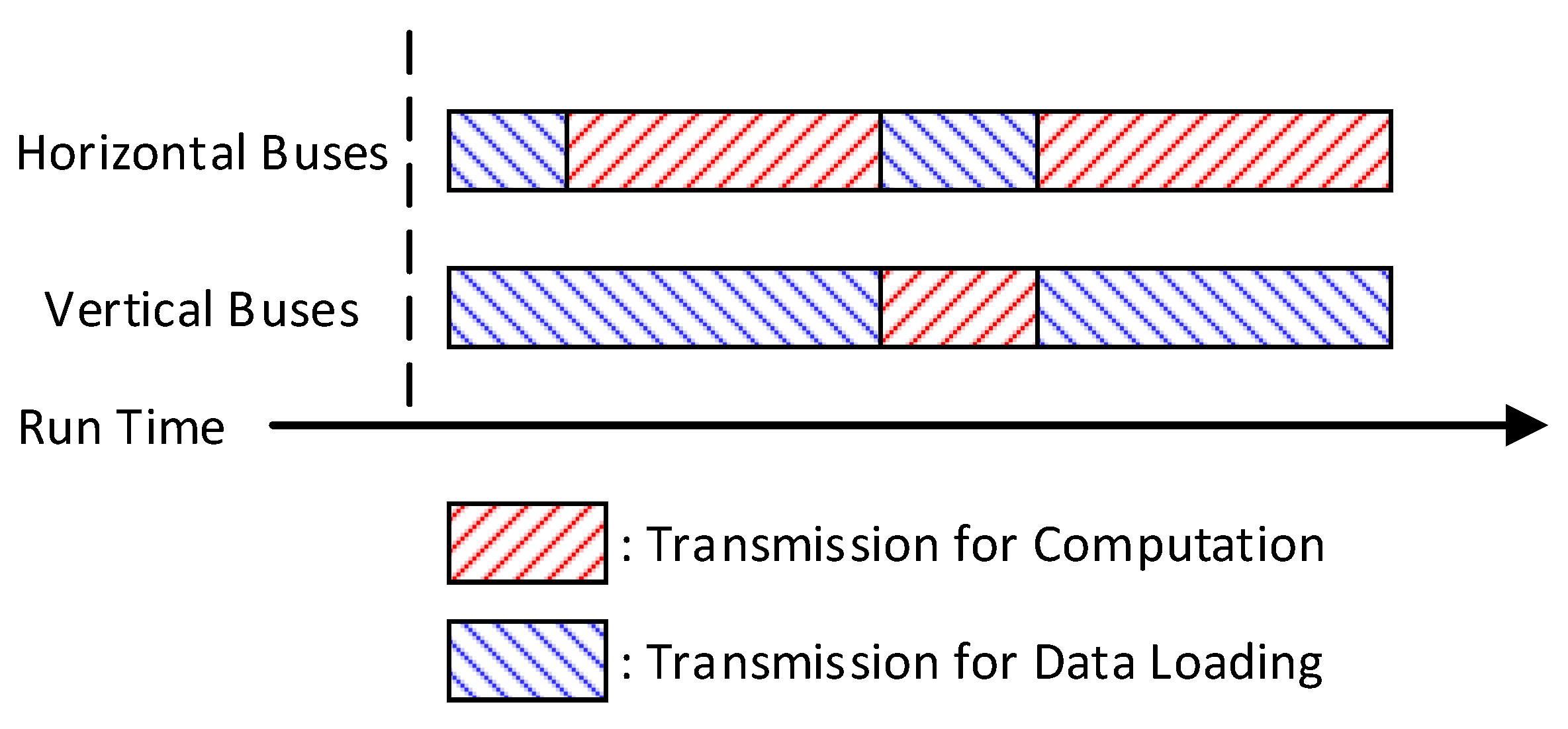
Section 3, the above buses are also used for data transmission when computing the 2D convolution with a kernel size larger than one. However, data transmission to the left or to the upper MAC units for computation will never happen simultaneously. This means there is always at least one group of buses free for data loading in each cycle. Additionally, when the MAC obtains data from the local memory, all the buses are free.
Generally, with a filter size of k × k and stride of s, in each k
2 cycle for convolution computation, there will be k × s cycles on the horizontal buses and k
2 + s
2 − k × s cycles on the vertical buses free for data loading. Therefore, the PE array can load new input activations along with the computation on the activations already loaded, as shown in
Figure 9. In particular, the data loading for the next input block can be synchronous with the computation on the current input block. Additionally, the old input patch will be replaced immediately after its last computation.
By this means, when the PA array starts to process a new input block, some input patches have been already stored in the MAC memories. Additionally, the rest of the input patches will be loaded during the processing of the first output channel. If the data loading cannot keep pace with the computation, then compute the other output channels on the patches already loaded. In the meantime, data loading continues until the entire input block is loaded. Additionally, the PE array will also finish the computation of the first few output channels by then and be ready to compute the rest. Therefore, the PE array can compute the CILs seamlessly, without any suspension for data loading.
This technique also works when there are no already loaded data to compute in the MAC memories. For example, for a CIL with a 3 × 3 filter and a stride of two, it will take 28 cycles to load two input patches 28 × 28 in size into the PE array. The computing is not executed here and both groups of buses are used for data loading. Then, the PE array finishes two 3 × 3 convolutions for an output channel on those two patches in 18 cycles. Meanwhile, only 14 × 14 activations of the next input patch are loaded through vertical buses and 12 × 14 activations of another input patch are loaded through horizontal buses. Therefore, the PE array has no new input patch to process and has to wait. As illustrated in the above-mentioned technique, in a case such as this, the PE array will compute the other output channels on the two loaded patches until the third input patch is loaded. Then, process the third input patch for the above output channels while loading the fourth input patch. Repeat these steps until all the input patches are loaded into the PE array.
It should be noticed that more time in each k2 cycles can be used to load activations through the vertical buses than the horizontal buses. The sequence of the patch loading on each bus is determined in line with the transmission speeds.
4.4.4. The Fused Pipeline to Process the Depth-Wise Convolutional Layers on the PE Array
Since the depth-wise convolutional layers do not reuse the input channels, the above technique is not effective for them on the PE array. However, each depth-wise output fmap is computed on only one input fmap generated by the CIL. Therefore, we can insert the computation of the depth-wise convolutional layer into the processing of the CIL.
An input patch for the depth-wise convolution will be stored in the MAC units directly after being generated or reloaded during the processing of the CIL. The PE array can suspend the computation of the CIL and compute this patch for depth-wise convolution first. After this, the PE array will revert back to processing the CIL, and this patch can be replaced by a new input patch for depth-wise convolution. This technique fused the processing of a CIL and the following depth-wise convolutional layer. The PE array can execute this computation when the CIL is not finished and other output fmaps have not been generated. It can solve the data loading problems of the depth-wise convolutional layers and keep the PE array computing seamlessly with high utilization. It also removes the most data throughput of the external memory in the depth-wise convolutional layers.
4.5. Techniques to Reduce the Data throughput with the External Memory
Once the input activation blocks are stored in the PE array, they will not be overwritten by new data until the convolution computation based on them for all output fmaps is finished. This can eliminate the repeated loading of input activations, especially from the external memory.
A coordinative kernel needs to be stored in the weight buffer to compute one output patch. Then, it can be overwritten by the next kernel. However, more than one input block may be stored in the PE array. For example, the PE array can store four input blocks of 256 × 14 × 14 activations with the 1-KB MAC memories. In this case, four patches of each output channel will be computed in succession with the shared kernel. This reuses a kernel four times, which can highly reduce the data throughput of the external memory.
4.6. The Pipeline Strategy for the Vision Tasks
The ALUs and MAC memories are used for both the ISP and the CNN processing; therefore, they are time-shared in the workflow. When processing the CNN, ALUs play a very minor role, which account for only 7.6% of the total cycles. Therefore, there is plenty of time for ISP to use the ALU array. The use of MAC memories is a priority for CNN processing to avoid the repeated loading of the input activations. For ISP, the data will be stored in the different memory modules with priorities in the following order: the Regs in ALU, memories in adjacent MAC units, the global buffer and the external memory. When the MAC memories are fully occupied by the CNN processing, ISP will skip them to the global buffer. Generally, the MAC memories have spare spaces for most of the time during the CNN processing. The ISP can make full use of them then. By these means, the ISP of the current frame and the CNN processing of the last frame can be carried out concurrently. The CNNs can use the outputs of ISP to accomplish the vision tasks in a pipelined way. Even though the ALUs are much less than the MACs, the ISP can still keep pace with CNN processing because the ISP tasks consume much less time.
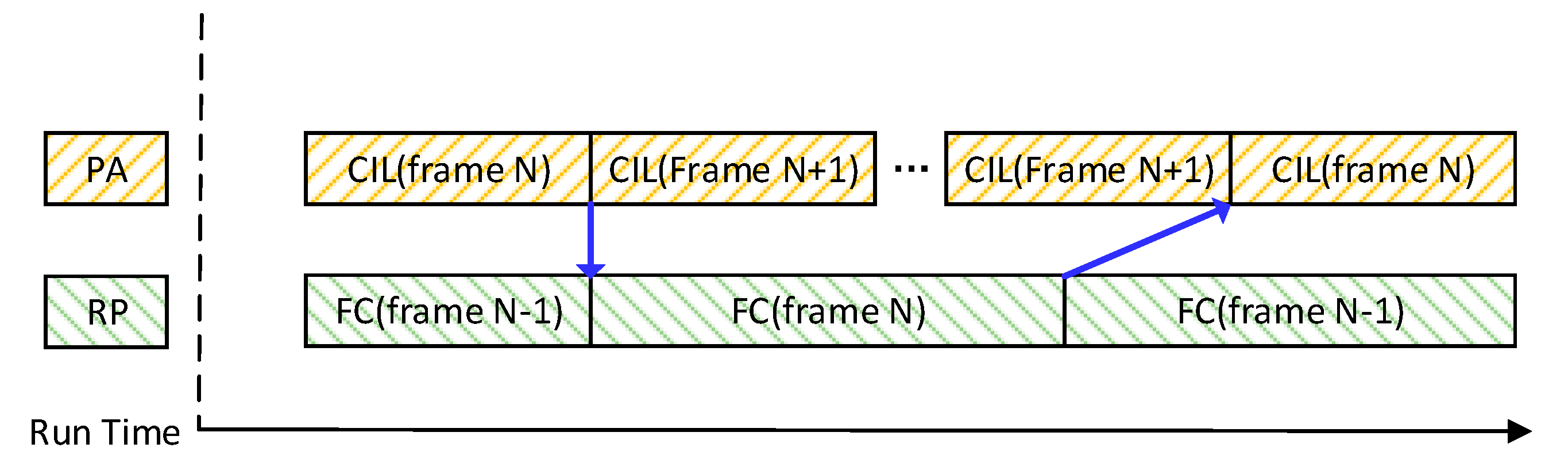
During the CNN processing, the CIL and MIL will also be processed in parallel, usually for different frames of images. When the CIL of the Nth frame is executed on the PE array, the Row processor will be processing the FC layers of the (N − 1)th frame simultaneously. Meanwhile, the ISP of the (N + 1)th frame will also be carried out on the ALU array. The Finite-State controller arranges the pipeline with the interrupt operations. By this means, the VPU can process the complex vision tasks seamlessly with a high utilization of hardware resources.
4.7. The Compilation
The workflow detailed above is the accurate procedure to compile a task on the VPU. Given a vision task with the specific ISP and CNN processing, the instructions to execute each subtask will be generated. Then, they will be sequenced based on the pipeline strategies. The generation of the instructions will consider the characters of both the tasks and the resources of the VPU. The instruction contains a specific operation for each module on the VPU. Additionally, the Finite-State controller will convert the instructions to control the signals for each cycle.


