Article

Optimized Design of a Sonar Transmitter for the High-Power Control of Multichannel Acoustic Transducers

1
Department of Electrical Engineering, Pohang University of Science and Technology, 77 Cheongam-ro, Pohang 37673, Korea
2
Agency for Defense Development, No. 18, Jinhae-gu, Changwon-si 51678, Korea
*
Author to whom correspondence should be addressed.
Electronics 2021, 10(21), 2682; https://doi.org/10.3390/electronics10212682
Submission received: 4 October 2021 / Revised: 30 October 2021 / Accepted: 31 October 2021 / Published: 3 November 2021
(This article belongs to the Section Industrial Electronics)

Abstract

:
For driving multichannel underwater acoustic transducers, the integrated design of the transmitter based on the analysis of the widely distributed impedance should be considered. Previous studies focused on either the matching circuit or the fast resonant tracking control. This paper proposes the design and control methods of a sonar transmitter based on the analysis of the impedance distribution. For the transmitter design, the optimization method based on the particle swarm optimization (PSO) algorithm is proposed for estimating the equivalent and matching circuit parameters. The equivalent circuits of the transducer are more precisely designed by using the measured data in both air and water. The fitness function proposed in the matching includes special functions, such as the limitation and parasitic inductances. A comparison of the experimental and simulation results shows that the optimized matching design improved the power factor, and was similar to the experimental result. For the transmitter control, the constant power and voltage control (CPVC) and instant voltage and current control (IVCC) methods are proposed for the variable impedance load. The impedance variation range affects the rated power and rated voltage of the transmitter, and the rating range determines the initial modulation index (MI) of the pulse-width modulation (PWM) control. To verify the control method, an experimental setup including the multichannel acoustic transducers was established. As a result, the constant power and constant voltage were verified with the proposed control, and the instant voltage and current control also worked in the event that the instant voltage or current exceed their threshold values.

1. Introduction

In recent years, the applications of acoustic transducers and transmitters have been expanded for sonar, medical, communications, and industrial purposes [1,2,3,4,5,6]. The mechanical and acoustic operations of an acoustic transducer are generally expressed as an electrical equivalent circuit model [7,8,9]. An electrical equivalent circuit is necessary not only to understand the energy transfer phenomenon, but also to design a transmitter driving an acoustic transducer. Since an acoustic transducer is a complex impedance load, a matching/filter circuit between a transmitter and an acoustic transducer is required for minimizing reactance and reducing THD (total harmonic distortion) [4,10,11,12,13,14,15]. To utilize their load characteristics, various control methods have been studied for the transmitters driving transducers with variable impedance [2,16,17,18].
Most interesting studies about the impedance matching and the control have concentrated on the ultrasonic transducer applications. The resonance frequency tracking method is applied to transmitters for driving ultrasonic transducers, because high control speed is required to trace high-frequency operation above several MHz. Wang et al. proposed a novel fast resonance tracking control for ultrasonic transducers [1]; they utilized the fact that the angle of a resonance point shifted by moving a center point of a G–B curve is correlated with a shifted center point of the G–B curve. Wang et al. attempted to mathematically calculate a resonance frequency for finding the optimized matching point [2]. Cheng et al. utilized parallel resonance frequency tracking and applied ZVS (zero-voltage switching) to the transmitter by considering both the parasitic capacitance of switches and the circuit elements of a transducer [19]. An et al. proposed a genetic algorithm for the broadband matching of ultrasonic transducers [20]; they focused on the optimization method to estimate the matching network topology.
In low-frequency applications, studies using a fast resonance frequency tracking cannot be found. Instead, most studies have concentrated on impedance matching and filter design. Choi et al. proposed an estimation method for simultaneously designing the matching and the filter circuits in sonar systems [21]; they focused on theoretical design, in order to apply parasitic elements of a transformer to the matching/filter circuits. To design a medium-voltage converter, it is important to consider the parasitic elements of the transformer, because the parasitic capacitance can affect its efficiency and control method [22]. Song et al. proposed the design method of matching and filter circuits by using only transformer magnetizing inductance [3]. Kim et al. proposed an LC matching technique for a class B amplifier driving high directional piezoelectric transducers [23]. Panchalai et al. designed a full-bridge inverter, and applied PWM (pulse-width modulation) for active sonar applications [16].
As can be seen in previous papers, studies of sonar transmitters have not presented a variety of views beyond ultrasonic transmitters. Recently presented papers have focused on either the matching/filter design or the PWM control, but not shown the integral system [3,16,21]. This paper presents the design and control of a sonar transmitter for the widely distributed impedance load to which the study field is generally inaccessible. The underwater acoustic transducer was developed to be driven both in multiple channels and in high-power conditions for achieving the detection ability of active sonar systems [3,17,24,25,26]. To control phases of transmission signal among transducers, the transducers are required to be independently driven [17]. To individually drive each transducer, it is necessary to consider impedance characteristics varied by the transmission signal types and mutual radiation effect. The interference effect by mutual radiation among transducers increases the range of impedance variation [27,28]. The large impedance range makes the power rating of the transmitter increase, but the transmitter’s specifications—such as size and rated power—are limited in real sonar systems. To satisfy higher acoustic source levels in the limited system, the major design elements of the transmitter should be considered, such as the limited supply of power, the maximum power driving the transducers, and the low THD [29]. In this paper, the following three issues are dealt with n designing the sonar transmitter:
(1)
In underwater acoustic transducers, the analysis of the impedance distribution is required in order to determine the rated power for driving the transducer;
(2)
To maximize the power factor (viz. minimizing reactance elements) and reduce THD, the impedance matching and filter circuits should be designed based on the equivalent circuit model of the transducer;
(3)
The frequency modulation (FM) is required in order to calculate the distance between a source and an object. The impedance of the transducer varies depending on the FM. For this reason, the output power of the transmitter should be maintained in the operation range.
This paper presents the design and control methods of the sonar transmitter, considering the three issues for driving the underwater acoustic transducer. There are two parts: the hardware design, and the control method. In Section 2, the impedance distribution of the multichannel acoustic transducers (MCATs) is analyzed for calculation of the rated power and the rated voltage of the transmitter. Based on the analysis of the impedance variation range, the hardware design process is described in Section 3. The circuit parameters of the acoustic transducer are estimated by using the PSO (particle swarm optimization) algorithm. The measured impedance is from a single transducer with a medium value in the distributed impedance. The proposed estimation method is different to the recently presented method in [30], with regard to the utilization of the impedances measured in air and water for more precise estimation. To find the parameters of the matching circuit, the new fitness function of the algorithm is proposed. The fitness function can find the optimized power factor, including parasitic elements, by limiting maximum magnetizing inductance. Afterwards, an LC filter considering all inductors and capacitors in the full circuit design is designed. In Section 4, UPWM (unipolar PWM) control is employed for the sonar transmitter with low THD. The constant power and voltage control (CPVC) and the instant voltage and current control (IVCC) are proposed for driving the MCAT. The modulation index (MI) is determined by the rated power and voltage obtained from the analysis of the impedance distribution. For fast control, the control command is determined and is applied to the full-bridge inverter, by calculating the root-mean-square (RMS) power and voltage within a single pulse period.

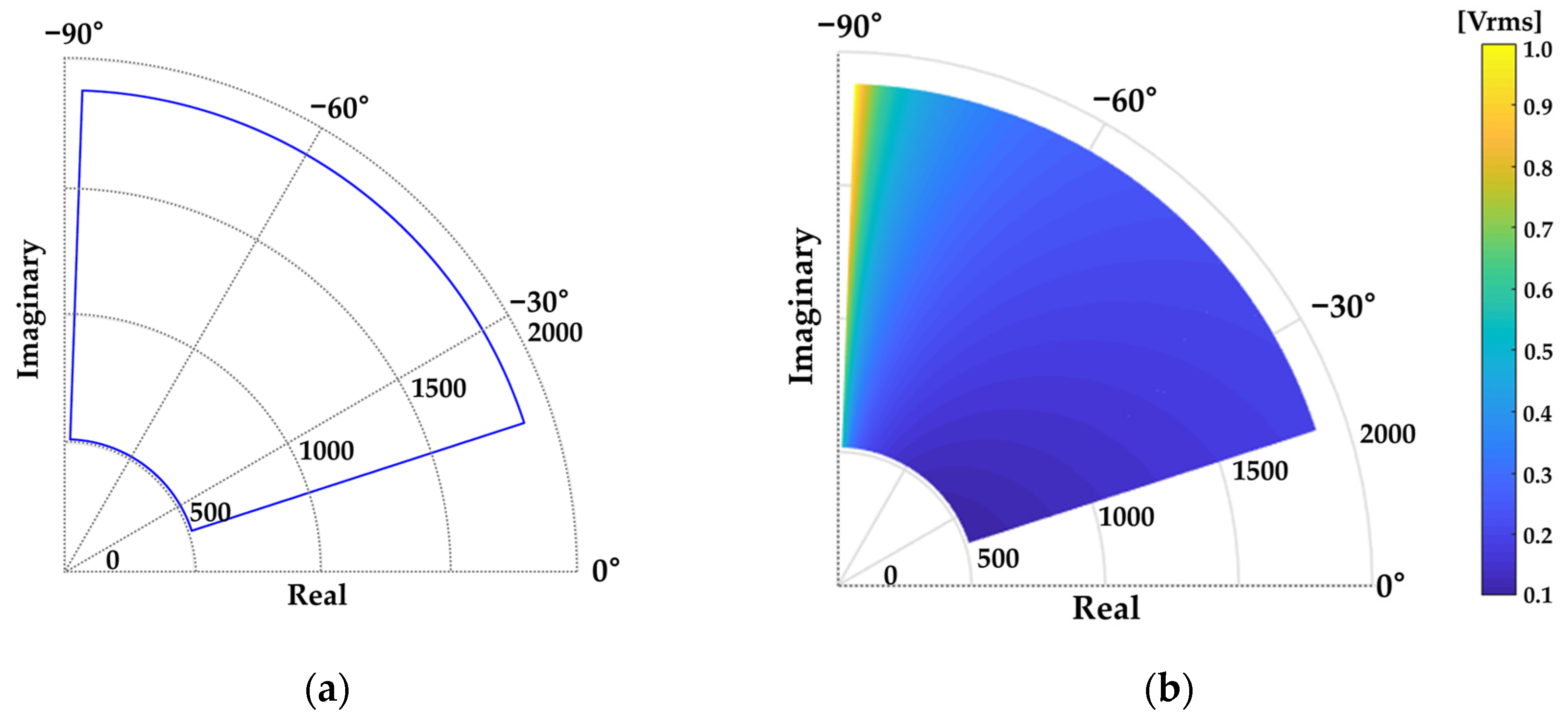
2. Analysis of the Impedance Distribution

The impedance of the transducer largely varies depending on the frequency modulation (FM), because of its reactance. When driving the MCAT, the impedance variation becomes large due to the interference effect by mutual radiation, individually driving transducers. Figure 1 shows the distributed impedance and the output voltage range of the MCAT. The impedance magnitude and phase are measured in the operation frequency band. The maximum and minimum impedance values can be identified via the impedance distribution. The impedance magnitude and phase have ranges from around 517 to 1880 (Ω) and −18° to 88°, respectively. To calculate the power rating of the transmitter, the required output voltage is analyzed in Figure 1b. The required source level determines the output power driving the transducers. From the required output power and the impedance distribution, the required output voltage range is calculated. The normalized voltage, 0.1, and 1 have 10 times this value, which is too large a range to design the transmitter. In this paper, the output voltage driving a single transducer is defined as the normalized voltage—0.14. The remaining area of the distribution can be covered by the matching circuit and the proposed control.

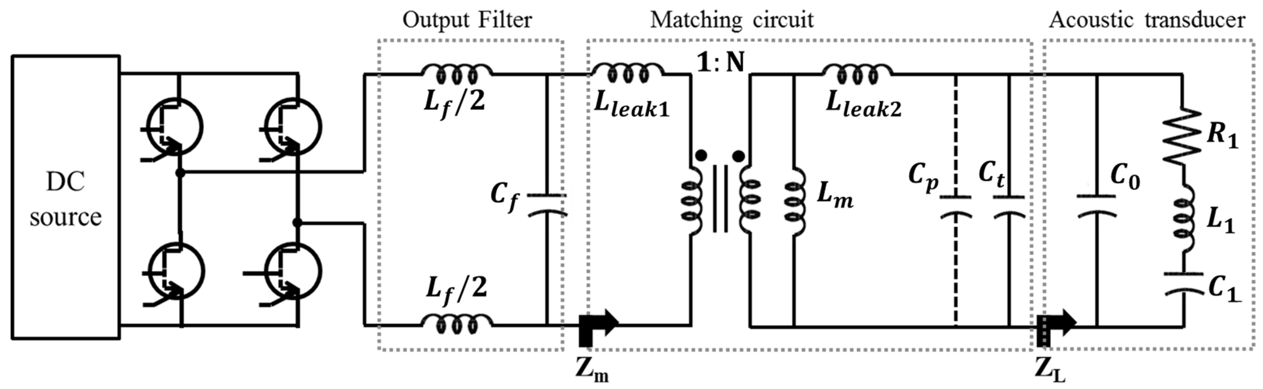
3. Design of the Sonar Transmitter

3.1. Design Process

To design the sonar transmitter, the circuit diagram is shown in Figure 2. Here, the BVD (Butterworth–Van Dyke) model is used for the equivalent circuit model of the transducer [3,9,21]. The transmitter’s topology consists of the full-bridge inverter converting DC to AC, a low-pass output filter reducing THD, and a matching circuit using a magnetizing inductance of the transformer. The design process is sequential, following the circuit modeling of the acoustic transducer, the matching circuit design, and the filter design. To cancel out the large reactance of the acoustic transducer, the transmitter should consider the operation frequency band. Generally, L1 and C1 disappear at the resonant frequency, but C0 still remains. The inductances of the matching circuit should be designed to cancel C0. From the inverter’s point of view, both the matching circuit and the transducer are loads.

3.2. The Acoustic Transducer

3.2.1. Estimation of the Equivalent Circuit Parameters
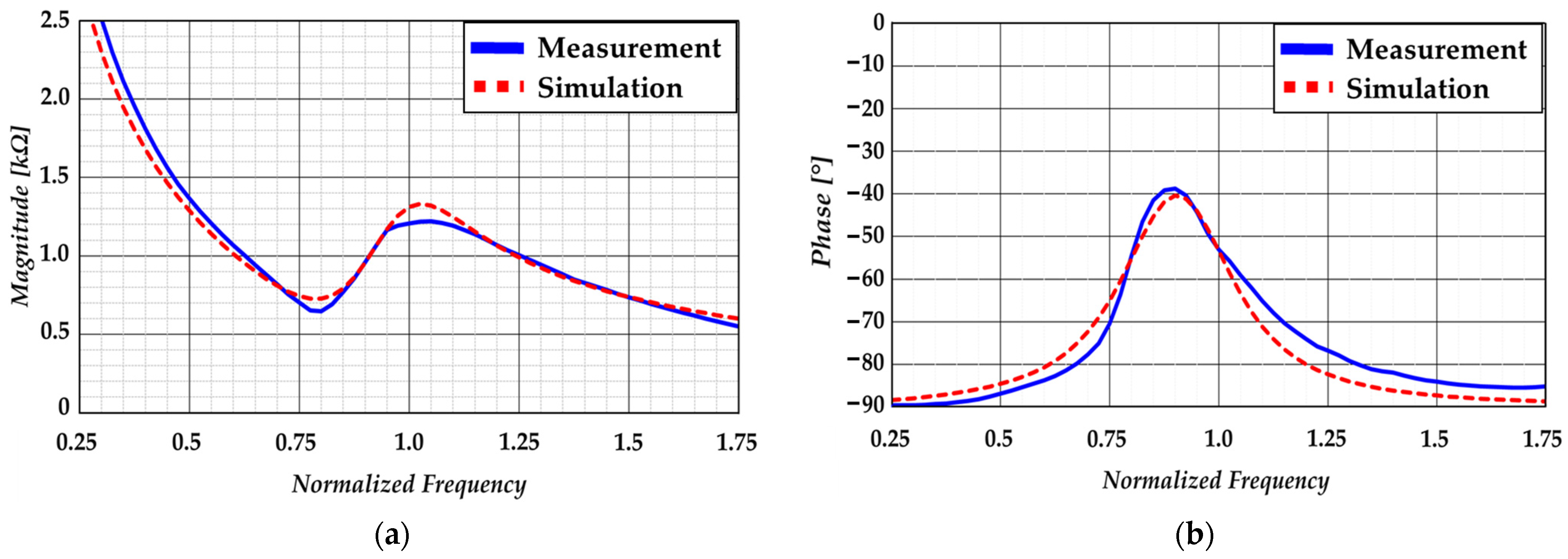
To design the matching circuit, the equivalent circuit model of the acoustic transducer is required in the operation frequency band. This chapter estimates the circuit parameters of the BVD model, as shown in Figure 2. The optimization method uses the fitness function that can well estimate the complex impedance at the resonance point. The fitness function, FEM, is expressed in Equations (1) and (2):
Z e ( n ) = α e ( n ) + j β e ( n ) ,     Z L = α L ( n ) + j β L ( n )
F E M ( n ) = 1 M f n = 1 M f | Z e ( n ) Z L ( n ) | = 1 M f n = 1 M f ( α e ( n ) α L ( n ) ) 2 + ( β e ( n ) β L ( n ) ) 2
where Mf is the total number of data samples of the measured impedance, n is a data sample in the frequency band, α(n) is the real impedance term of the transducer for the n-th data sample, and β(n) is the imaginary impedance term of the transducer for the n-th data sample.

3.2.2. Results

Figure 3 shows the estimated and measured impedance magnitude and phase. The estimated impedance corresponds with the measured impedance. The estimated impedance, Ze, is calculated using the measured impedance, ZL, both in the air and underwater. The estimation method of the equivalent circuit parameters generally uses the measured underwater data, but this paper presents a method using both air and underwater data for accuracy. First, the method finds the electrical capacitance, C0, and the stiffness, C1, of the transducer from the measured data in the air, and then the other parameters are estimated from the measured underwater data. The test unit is the piezoelectric tonpilz transducer. The impedance magnitude and phase were measured by an impedance analyzer (4194A, HP) at intervals of 100 Hz. The estimated circuit parameters are shown in Table 1.

3.3. The Matching Circuit

3.3.1. Estimation of the Matching Circuit Parameters

This chapter discusses the design of the impedance matching circuit for minimizing the reactive power in the driving transducers. The deviation in the reactance values of the transducers becomes large due to the FM in the MCAT. Of course, it is good to design a matching circuit for each transducer, but this is not realistic with a large number of transducers. Thus, this paper designed the matching circuit for a single transducer located in the medium of the impedance distribution. The impedance matching circuit utilizes a transformer consisting of the magnetizing inductance, Lm, and leakage inductances, Lleak1 and Lleak2, to reduce the reactance capacitances, C0 and C1. Therefore, the matching circuit maximizes the power factor to drive the transducers in the operation frequency band.
The elements in the matching circuit are estimated based on the PSO algorithm. The coupling coefficient of the transformer, kp, is defined as 0.98, and the winding resistance is ignored, but the magnetizing and leakage inductances of the transformer are estimated from the algorithm. In the ~0.5∙fn (Hz) frequency band (fn is the fundamental frequency in the band), the algorithm is set to find the maximum power factor, and to minimize the magnetizing inductance. The fitness and its related functions are expressed in Equations (3)–(8). Table 2 shows the parameters for Equations (3)–(8). The fitness function includes a selection function to choose the lowest inductance among the estimated inductances, in consideration of the transmitter size. Here, C1 and C2 are weight factors that are empirically determined in consideration of the parameter range and the iteration speed (C1 = 1, C2 = 1).
F M C ( n ) = n = f s f s + B W c 1 · F p f ( n ) + c 2 · F L ( n )
F p f ( n ) = 1 p f ( Z m ( n ) ) , F L ( n ) = L m
Z m ( n ) = ω 2 G L d Z L m + j ω { ( L m + N 2 L l e a k 1 ) ω B L d Z L m } N 2 [ { 1 ω B L d ( L m + L l e a k 2 ) } + j ω G L d ( L m + L l e a k 2 ) ]
Z L m = L m L l e a k 2 + N 2 L l e a k 1 ( L m + L l e a k 2 )
Y L d ( n ) = G L d + j B L d = 1 R 1 ( 1 + Q 1 2 γ 2 ) + j { ω ( C 0 + C d ) ω s C 1 Q 1 2 γ 1 + Q 1 2 γ 2 }
ω s = 1 L 1 C 1 ,     Q 1 = ω s L 1 R 1 , γ = ω ω s ω s ω
where Zm is the impedance calculated on the input side of the impedance matching, and includes leakage inductances of the transformer and the output capacitance, Ct, of the transmitter as shown in Figure 2. The output capacitance is considered to be 3.4 (nF). The turn ratio of the transformer is ~1:3.6 for boosting the input voltage. As a result, the estimated magnetizing inductance is 50.9 (mH), and the estimated leakage inductance 1 and 2 are 73.6 (μH) and 0.98 (mH), respectively, while a parasitic capacitance between the transmitter and the transducer, Cp, in Figure 2 is ignored in the estimation of the impedance matching.

3.3.2. Experimental Setup

To compare the simulation and the experiment of the designed matching circuit, the test system was set up. The test system consisted of the designed matching circuit and a transducer in the water. The magnitude and phase of the input matching impedance, Zm, were measured using an impedance analyzer (4194A, HP) at intervals of 100 Hz. The power factor was calculated by using the phase. All experimental data were measured from the input terminal of the test system.

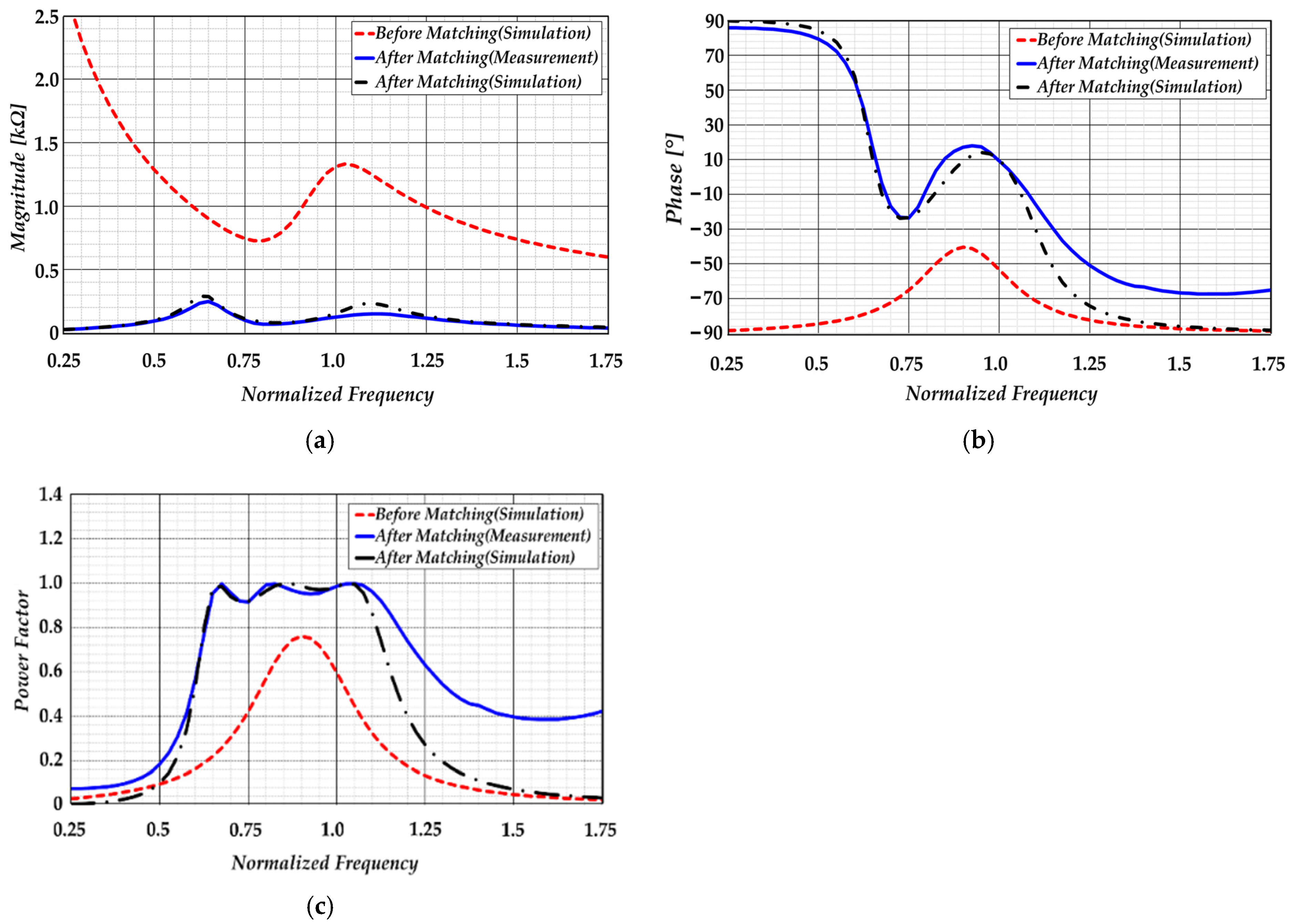
3.3.3. Experimental Results

Figure 4 shows the impedance and the power factor before and after applying the matching circuit. The estimated impedance and power factor after applying the matching circuit were compared to the measured value. After impedance matching, the impedance magnitude was more uniform and smaller in the operation frequency band, compared to the case before impedance matching. Moreover, the impedance phase is near zero, and the power factor has a uniform value above 0.9 in the operation frequency band. It was identified that all estimated values corresponded to the measured values. Within or out of the operating frequency, differences between the measured and estimated results can occur because of the influence of other adjacent resonance modes.

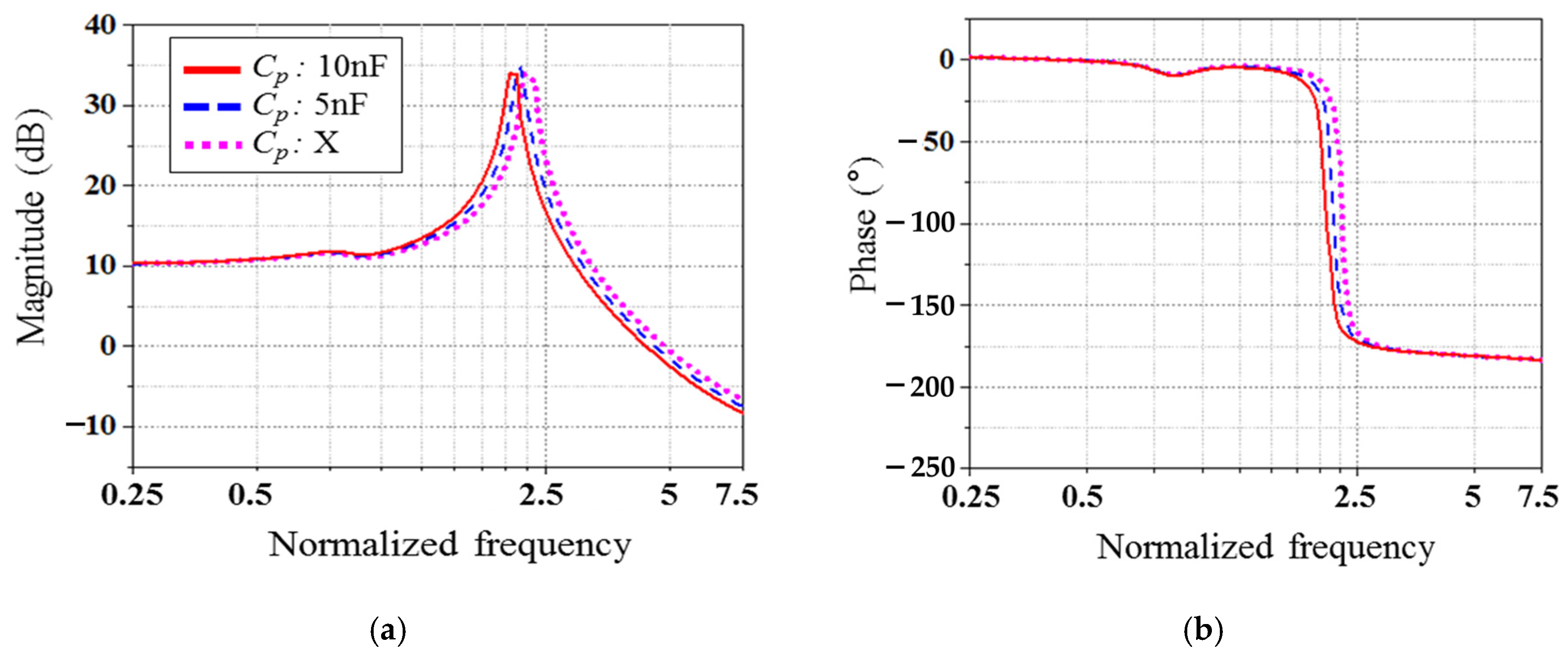
3.4. The LC Filter Circuit

The low-pass filter on the output side of the full-bridge inverter is necessary to eliminate the THD of the transmission signal. The real acoustic energies are radiated through the resistance of the BVD model. Thus, the LC parameters of the BVD model and the matching transformer are utilized in designing the filter circuit. The cutoff frequency, fc, is ~2.175∙fn (Hz) for the UPWM inverter in the operation frequency band. The inductance, Lf, and capacitance, Cf, are 400 (μH) and 94 (nF), respectively. Figure 5 shows the analysis of the transfer function from the filter to the BVD model. The cutoff frequency can be moved by the parasitic capacitance value, Cp. The results show that the parasitic elements can be utilized for a filter design, and that the cutoff frequency is located at the intended point.

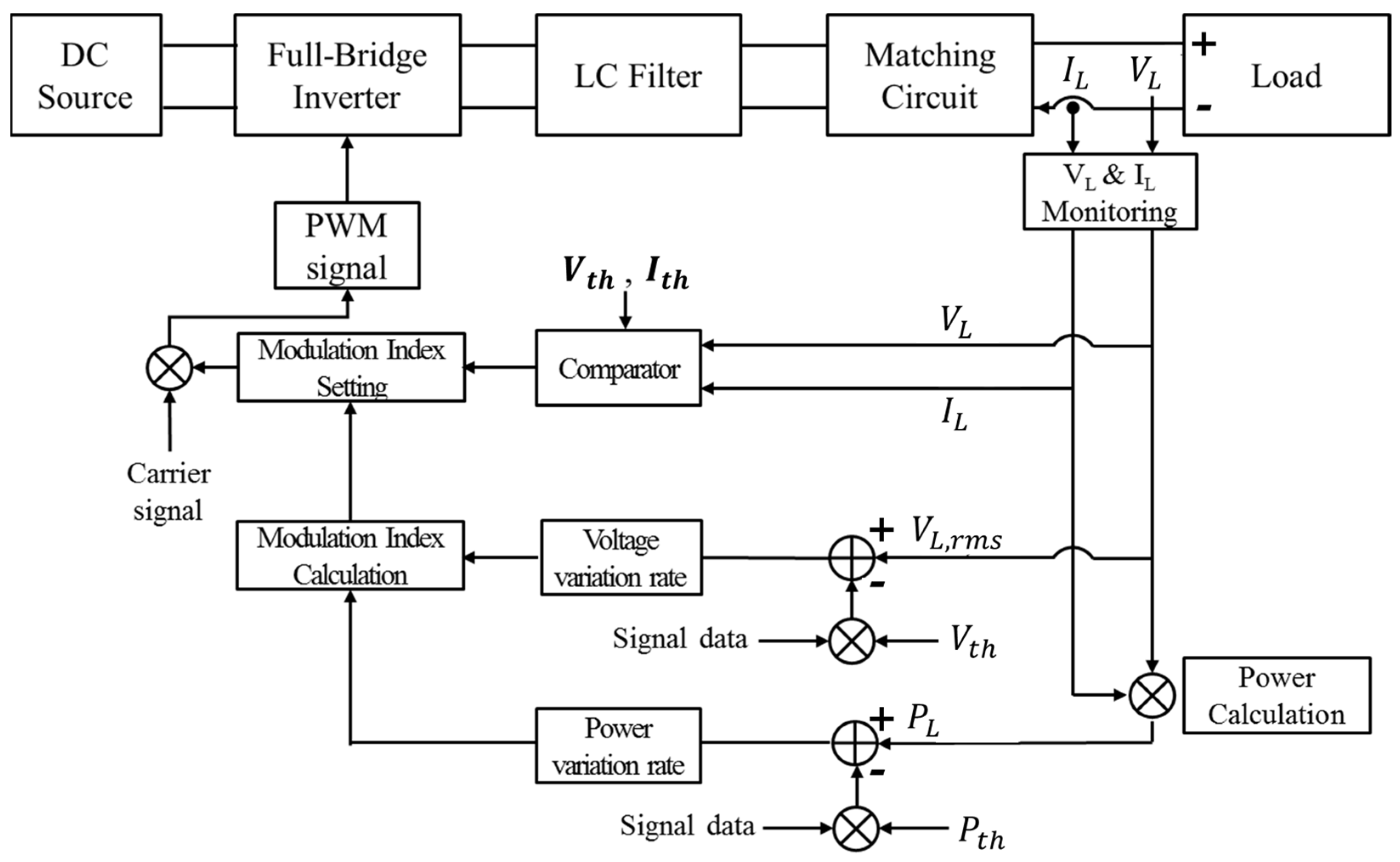
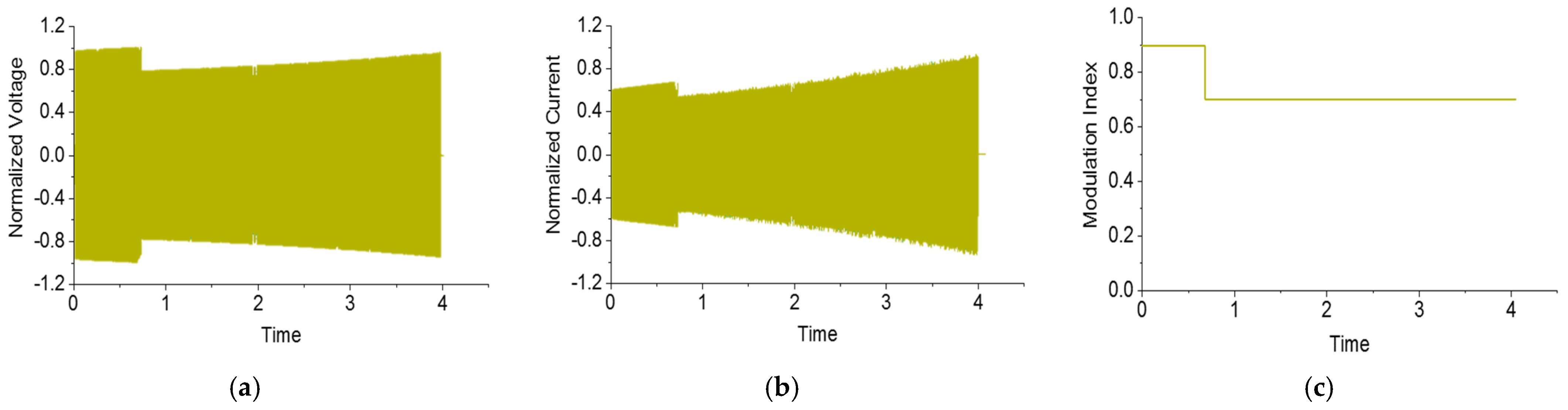
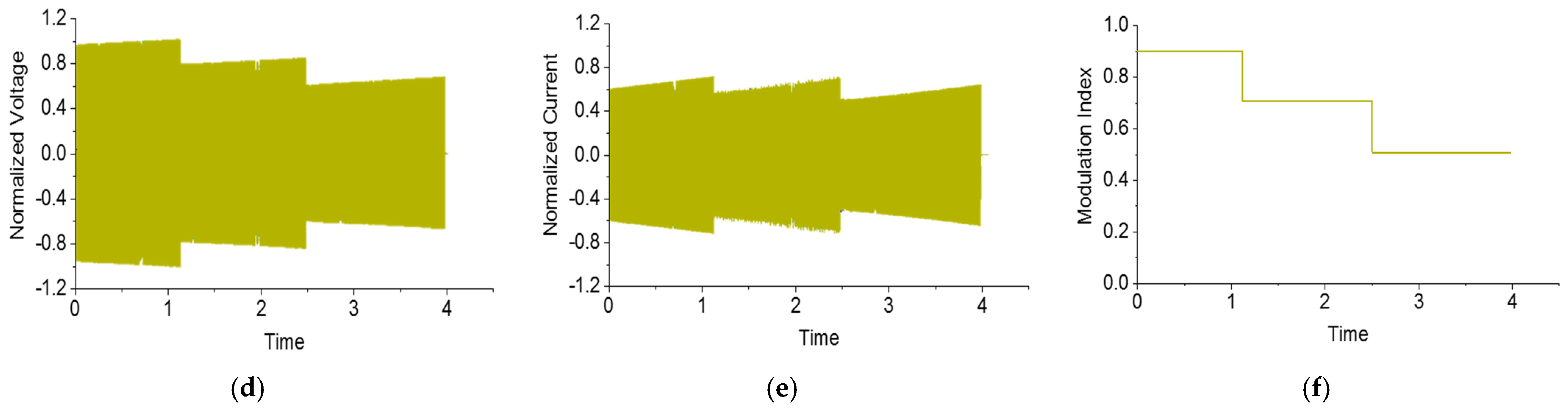
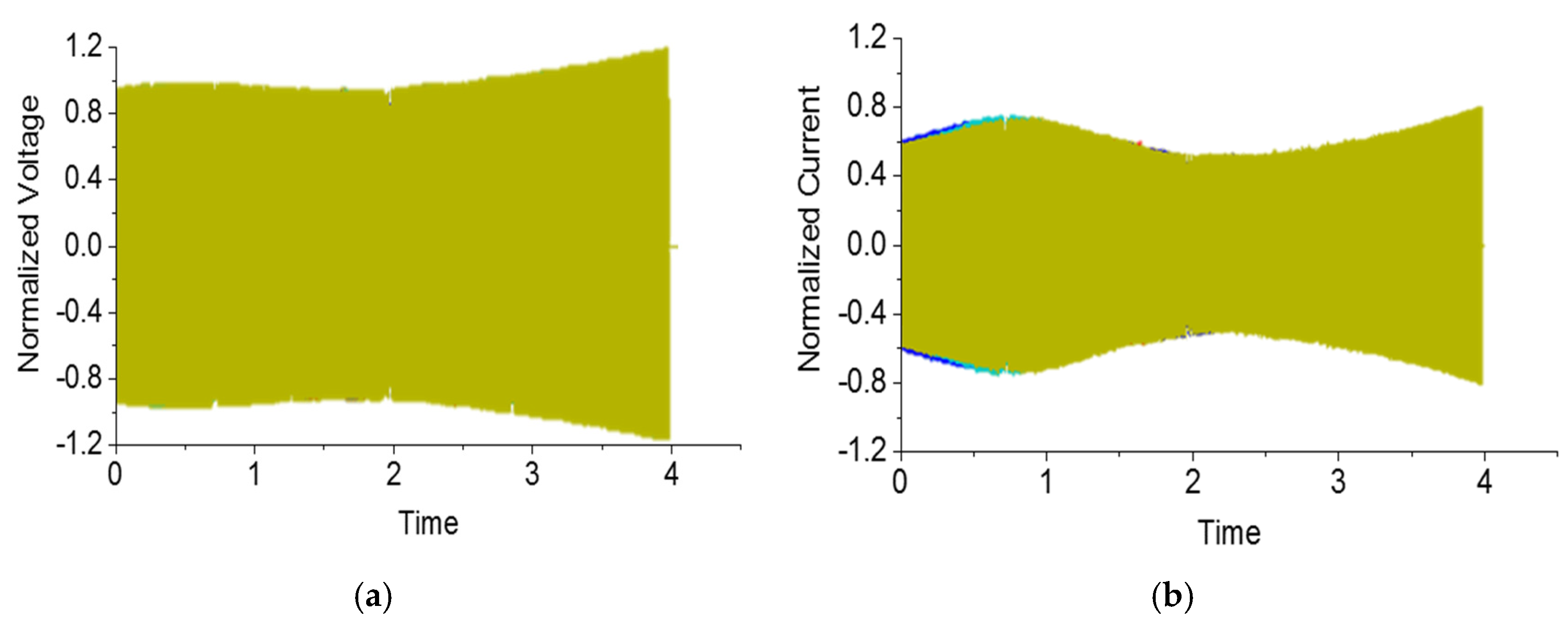
4. The control of the Sonar Transmitter

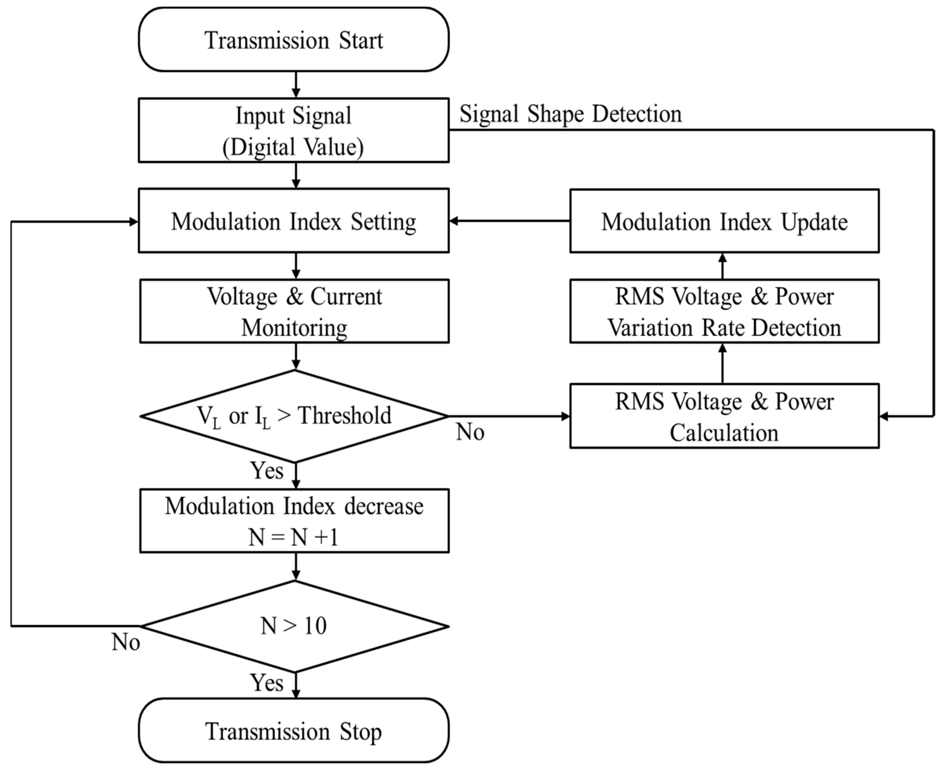
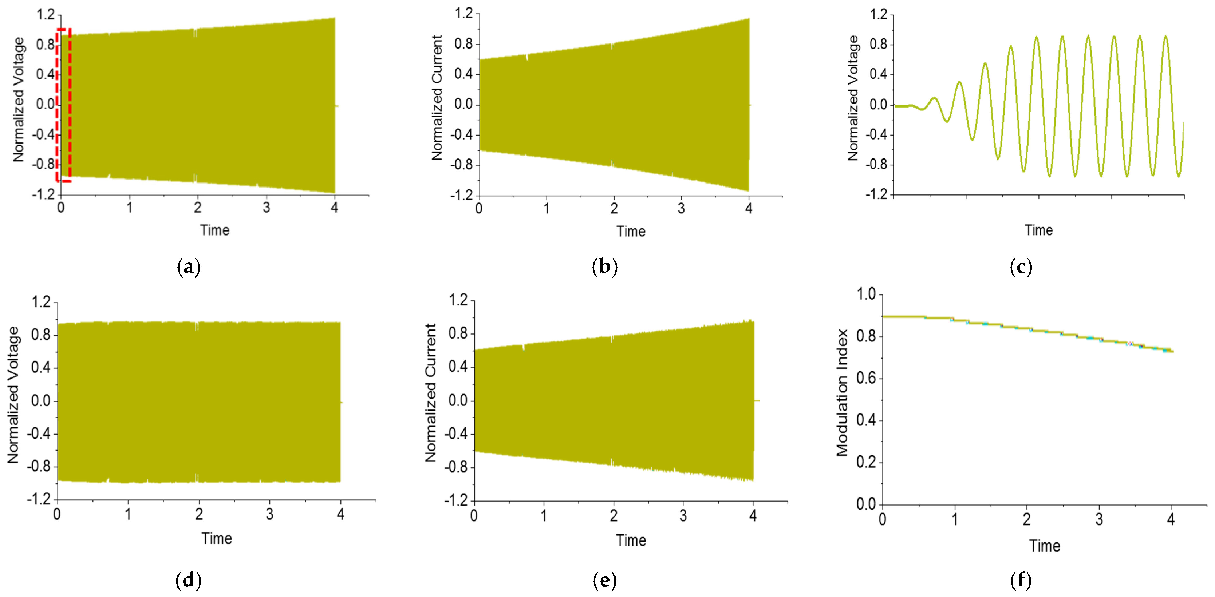
4.1. The Control Method

The control of the transmitter output is proposed for the MCAT. Figure 6 shows the proposed control block diagram in the variable impedance condition. The proposed control of the transmitter is based on the UPWM. The monitoring circuit detects the output voltage, VL, and current, IL, in real time, and calculates the output power per single pulse period of the transmission signal. The detected power and voltage are compared with the threshold power, Pth, and voltage, Vth, including the information of the transmission signal, and then the deviation is calculated. From the deviation, the variation of the modulation index (MI) is expressed in Equation (9).
Δ M I = δ × P o u t P t h P t h  
where, Pout is the output power, Pth is the threshold power, and δ is the weight factor obtained by considering a convergence time of less than 1 (ms) and an overshoot of less than 5 (%) by the experimental experience. The initial MI can be calculated from the required output voltage, as expressed in Equation (10). The updated MI is set as expressed in Equation (11).
I n i t i a l   M I = T h e   r e q u i r e d   o u t p u t   v o l t a g e D C   s o u r c e   v o l t a g e × t r a n s f o r m e r   r a t i o   ( 3.6 ) × 0.707 ( f o r   R M S )
T h e   u p d a t e d   M I ( n ) = M I ( n 1 ) + Δ M I
The PWM signal is obtained by comparing updated MI and carrier signal control values to switches of the full-bridge inverter. In real time, if a transient output voltage or current occurs due to the rapidly varied impedance, the proposed method constantly transmits lower level signals. This function limits the power rating of the transmitter to protect the transmitter from the variable impedance load. Figure 7 shows the algorithm flowchart of the proposed control method. The details are explained as follows:
(1)
Sets the input signal and detecting the signal shape in the time domain;
(2)
Defines the initial MI for PWM control;
(3)
Detects the output voltage and current from the monitoring circuit;
(4)
If the output voltage and current values are below the threshold, calculates the RMS power and RMS voltage per single pulse period, and then updates the MI by adding the MI variation (delta MI) to the previous MI;
(5)
If the output voltage and current instantly exceed the threshold, reduces the MI by 0.2 per single pulse period (if this operation is performed more than 10 times, the transmitting signal will be blocked for protection of the transmitter).

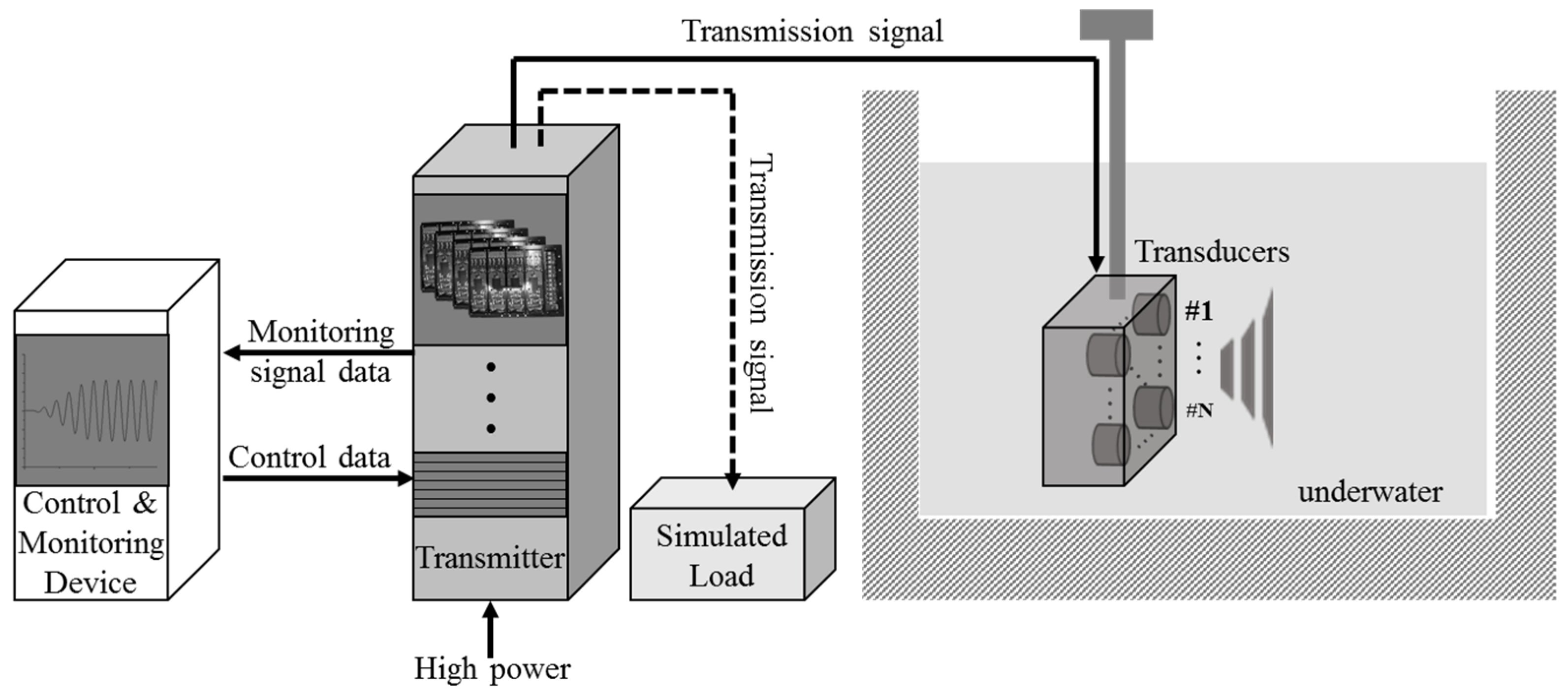
4.2. The Experimental Setup
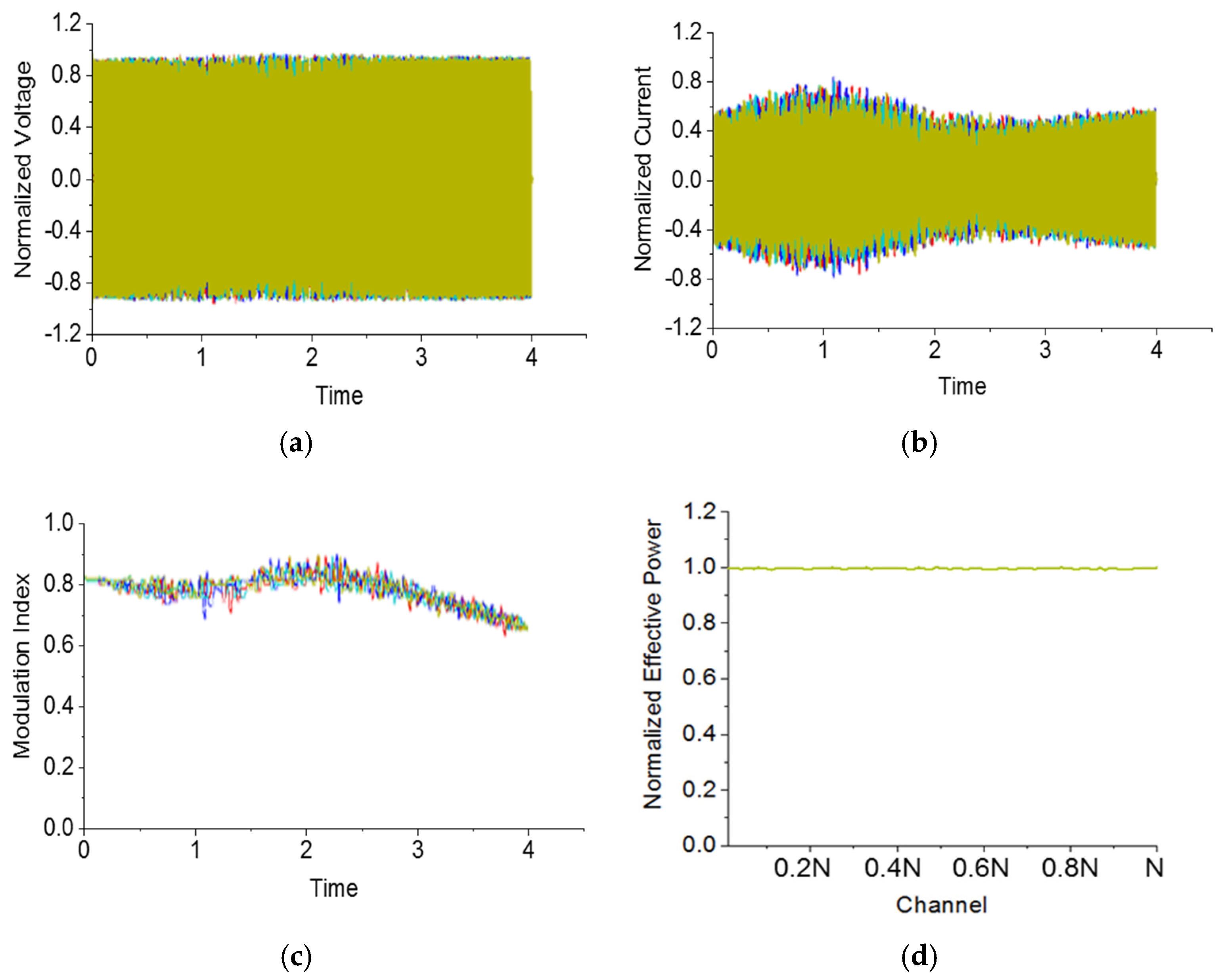
The experimental setup of the transmitter control using the simulated load and the MCAT load is illustrated in Figure 8. The experimental system consists of the control and monitoring device, the designed transmitter, the simulated load, and the MCAT in the water tank. The transmitter consists of the full-bridge inverter, the LC filter, and the matching transformer. As shown in Figure 2, the transmitter is set up using the designed parameters above. The GaN MOSFETs are used for fast switching.
The verification of the control operation was performed in both the simulated load and the MCAT load. (1) To verify the proposed control method, the simulated load was set up to express the operation of a single channel unit. The simulated load consists of the resistor and capacitor in parallel, so that the load is similar to the impedance of the interest frequency point. The RC load was used to check the exact operation in the transmitter control test [3]. (2) The real multichannel acoustic transducer (MCAT) load was established so as to verify that the proposed control reduces the impedance variation caused by the FM. The MCAT consists of multichannel transducers; the number is N. The proposed control used a transmitting FM signal. The threshold values of the CPVC and IVCC were set for the output characteristics in the MCAT.

4.3. Results

4.3.1. The Experiment Using the Simulated Load

Figure 9 shows the output voltage and current with or without the control in the simulated load. To show the impedance variation of the load, the FM is used for each control condition, and the voltage and current are normalized in each maximum value. The output voltage and current increase without the control, as shown in Figure 9a,b. Figure 9c shows the enlarged output voltage for identifying the sine waveform. Figure 9d–f show the output voltage and current with the constant power and voltage control (CPVC) in the simulated load. The graphs with the CPVC show that the output voltage remains constant, although the output current increases. Simultaneously, the MI decreases, limiting the output voltage. As a result, the proposed CPVC is well operated in the simulated load.
Figure 10 shows the output voltage and current limitation with the instant voltage and current control (IVCC) in the simulated load. The IVCC operates when the voltage and current immediately exceed the threshold. In this experiment, the limitation values of voltage and current were sequentially changed to verify their operation in the rapidly variable impedance. Figure 10a–c show the output voltage, current, and MI, respectively, in the instant voltage control operation when the output voltage exceeds the normalized threshold (Vnorm = 1.0). Figure 10d–f show the same values in the instant current control operation when the output current exceeds the normalized threshold (Ith = 0.7). As a result, the transmitter can stably transmit the signal via the sequentially lowered MI when the rapidly variable impedance affects the output voltage and current.

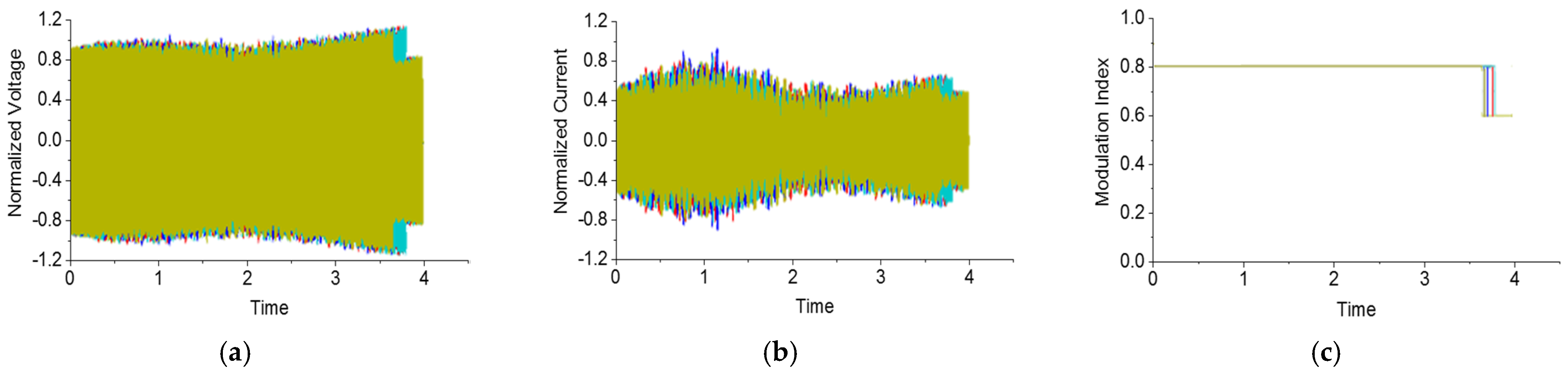
4.3.2. The Experiment Using a Multichannel Acoustic Transducer Load

Figure 11 shows the output voltage and current without any control in the MCAT load. The output voltage decreases by 2 s, and then increases again. This phenomenon occurs because of the impedance variation caused by the FM.
Figure 12 shows the output voltage and current with CPVC in the MCAT load. The impedance of the MCAT load changes with the FM signal. The MIs started at 0.8, as determined by Equation (10). After applying the CPVC, the constant power control is applied before 2.3 s, and the constant voltage control is applied after 2.3 s. As a result, the output voltage is constant, even if the output current varies in the variation impedance. For more information, the normalized power values at each transducer are shown in Figure 12d. The results show that constant power control is applied on each transducer.
Figure 13 shows the output voltage and current with IVCC in the MCAT load. The threshold condition is set to verify the IVCC. When the output voltage exceeds the normalized threshold (Vnorm = 1.1), after ~3.6 s, the controllers reduce their MIs from ~0.8, by 0.2 steps.

5. Conclusions

This paper presented both the matching/filter circuit design using the PSO algorithm and the control method of the sonar transmitter in the MCAT load. In the actual design of the sonar transmitter, it is very important to identify the impedance distribution of all acoustic transducers. Because the radiated acoustic energies affect the other transducers, the impedance variation can be large. For this reason, the design and control proposed in this paper refer to the range of the impedance distribution.
In the acoustic transducer of Section 3.2, a transducer with an impedance value located in the middle of the impedance distribution is converted to the electrical equivalent circuit. The estimation method considers the measured data from both air and water, in order to achieve better accuracy than previous estimation methods.
In the matching circuit of Section 3.3, a transformer with parasitic elements was utilized for matching to the transducer model. The proposed fitness function includes a significant difference to existing models, in that the fitness function can find the matching parameters for maximizing the power factor in the limited magnetizing inductance. The proposed method can avoid the finding of unrealistic design values. As a result, a matching transformer with a power factor above 0.9 in the operating frequency band was realized. Moreover, the experimental results coincided with the simulation. In the filter circuit of Section 3.4, LC parameters were selected by considering the designed matching circuit and the electrical equivalent circuit of the transducer together.
In the control of Section 4, CPVC and IVCC were proposed for minimizing the impedance variation caused by the FM signal type. The MI was selected by considering the required voltage in the impedance distribution. When increasing the modulated frequency, the transducer’s impedance fluctuated. CPVC can control the power and voltage constantly, while IVCC can limit the maximum voltage and current in real time. To prove the proposed controls, the RC simulated load and the real MCAT load were set up. As a result, the transmitter can keep the output power or voltage constant, and can instantly limit the voltage or current in the variable impedance load.
This paper offers a design and control method for the generally inaccessible condition of a large impedance distribution in the MCAT. The proposed design and the control method are expected to aid in the design of a full, active sonar system with multichannel acoustic transducers.

Author Contributions

Conceptualization, J.-E.B. and J.-M.L.; Data curation, B.-H.L.; Formal analysis, B.-H.L. and J.-M.L.; Investigation, J.-E.B. and D.-W.K.; Methodology, B.-H.L. and J.-E.B.; Project administration, J.-M.L. and J.-Y.S.; Resources, D.-W.K.; Software, B.-H.L.; Supervision, J.-Y.S.; Visualization, D.-W.K.; Writing—original draft, B.-H.L. and J.-E.B.; Writing—review & editing, D.-W.K., J.-M.L. and J.-Y.S. All authors have read and agreed to the published version of the manuscript.

Funding

This research received no external funding.

Conflicts of Interest

The authors declare no conflict of interest.

References

  1. Wang, J.-D.; Jiang, J.-J.; Duan, F.-J.; Zhang, F.-M.; Liu, W.; Qu, X.-H. A Novel Fast Resonance Frequency Tracking Method Based on the Admittance Circle for Ultrasonic Transducers. IEEE Trans. Ind. Electron. 2019, 67, 6864–6873. [Google Scholar] [CrossRef]
  2. Wang, J.-D.; Jiang, J.-J.; Duan, F.-J.; Cheng, S.-Y.; Peng, C.-X.; Liu, W.; Qu, X.-H. A High-Tolerance Matching Method Against Load Fluctuation for Ultrasonic Transducers. IEEE Trans. Power Electron. 2019, 35, 1147–1155. [Google Scholar] [CrossRef]
  3. Song, S.-M.; Kim, I.-D.; Lee, B.-H.; Lee, J.-M. Design of Matching Circuit Transformer for High-Power Transmitter of Active Sonar. J. Electr. Eng. Technol. 2020, 15, 2145–2155. [Google Scholar] [CrossRef]
  4. Rathod, V.T. A Review of Electric Impedance Matching Techniques for Piezoelectric Sensors, Actuators and Transducers. Electronics 2019, 8, 169. [Google Scholar] [CrossRef] [Green Version]
  5. Shen, J.; Luo, J.; Fu, S.; Su, R.; Wang, W.; Zeng, F.; Song, C.; Pan, F. 3D Layout of Interdigital Transducers for High Frequency Surface Acoustic Wave Devices. IEEE Access 2020, 8, 123262–123271. [Google Scholar] [CrossRef]
  6. Kobayashi, S.; Kondoh, J. Feasibility Study on Shear Horizontal Surface Acoustic Wave Sensors for Engine Oil Evaluation. Sensors 2020, 20, 2184. [Google Scholar] [CrossRef] [PubMed] [Green Version]
  7. Crupi, G.; Gugliandolo, G.; Campobello, G.; Donato, N. Measurement-Based Extraction and Analysis of a Temperature-Dependent Equivalent-Circuit Model for a SAW Resonator: From Room Down to Cryogenic Temperatures. IEEE Sens. J. 2021, 21, 12202–12211. [Google Scholar] [CrossRef]
  8. Bybi, A.; Mouhat, O.; Garoum, M.; Drissi, H.; Grondel, S. One-dimensional equivalent circuit for ultrasonic transducer arrays. Appl. Acoust. 2019, 156, 246–257. [Google Scholar] [CrossRef]
  9. Peng, X.; Hu, L.; Liu, W.; Fu, X. Model-Based Analysis and Regulating Approach of Air-Coupled Transducers with Spurious Resonance. Sensors 2020, 20, 6184. [Google Scholar] [CrossRef]
  10. Agbossou, K.; Dion, J.-L.; Carignan, S.; Abdelkrim, M.; Cheriti, A. Class D amplifier for a power piezoelectric load. IEEE Trans. Ultrason. Ferroelectr. Freq. Control. 2000, 47, 1036–1041. [Google Scholar] [CrossRef]
  11. Ju, B.; Shao, W.; Zhang, L.; Wang, H.; Feng, Z. Piezoelectric ceramic acting as inductor for capacitive compensation in piezoelectric transformer. IET Power Electron. 2015, 8, 2009–2015. [Google Scholar] [CrossRef]
  12. Huang, H.; Paramo, D. Broadband electrical impedance matching for piezoelectric ultrasound transducers. IEEE Trans. Ultrason. Ferroelectr. Freq. Control. 2011, 58, 2699–2707. [Google Scholar] [CrossRef]
  13. Cheng, H.-L.; Cheng, C.-A.; Fang, C.-C.; Yen, H.-C. Single-Switch High-Power-Factor Inverter Driving Piezoelectric Ceramic Transducer for Ultrasonic Cleaner. IEEE Trans. Ind. Electron. 2010, 58, 2898–2905. [Google Scholar] [CrossRef]
  14. Lin, S.; Xu, J. Effect of the Matching Circuit on the Electromechanical Characteristics of Sandwiched Piezoelectric Transducers. Sensors 2017, 17, 329. [Google Scholar] [CrossRef]
  15. Rathod, V.T. A Review of Acoustic Impedance Matching Techniques for Piezoelectric Sensors and Transducers. Sensors 2020, 20, 4051. [Google Scholar] [CrossRef]
  16. Panchalai, V.N.; Chacko, B.P.; Sivakumar, N. Digitally controlled power amplifier for underwater electro acoustic transducers. In Proceedings of the 2016 3rd International Conference on Signal Processing and Integrated Networks (SPIN), Noida, India, 11–12 February 2016; pp. 306–311. [Google Scholar]
  17. Choi, J.-H.; Lee, D.-H.; Mok, H.-S. Discontinuous PWM Techniques of Three-Leg Two-Phase Voltage Source Inverter for Sonar System. IEEE Access 2020, 8, 199864–199881. [Google Scholar] [CrossRef]
  18. Chacko, B.P.; Panchalai, V.N.; Sivakumar, N. Multilevel digital sonar power amplifier with modified unipolar SPWM. In Proceedings of the 2015 International Conference on Advances in Computing, Communications and Informatics (ICACCI), Kochi, India, 10–13 August 2015; pp. 121–125. [Google Scholar]
  19. Cheng, L.-C.; Kang, Y.-C.; Chen, C.-L. A Resonance-Frequency-Tracing Method for a Current-Fed Piezoelectric Transducer. IEEE Trans. Ind. Electron. 2014, 61, 6031–6040. [Google Scholar] [CrossRef]
  20. An, J.; Song, K.; Zhang, S.; Yang, J.; Cao, P. Design of a Broadband Electrical Impedance Matching Network for Piezoelectric Ultrasound Transducers Based on a Genetic Algorithm. Sensors 2014, 14, 6828–6843. [Google Scholar] [CrossRef] [PubMed] [Green Version]
  21. Choi, J.-H.; Mok, H.-S. Simultaneous Design of Low-Pass Filter with Impedance Matching Transformer for SONAR Transducer Using Particle Swarm Optimization. Energies 2019, 12, 4646. [Google Scholar] [CrossRef] [Green Version]
  22. Zhang, L.; Ji, S.; Gu, S.; Huang, X.; Palmer, J.E.; Giewont, W.; Wang, F.F.; Tolbert, L.M. Design Considerations for High-Voltage Insulated Gate Drive Power Supply for 10-kV SiC MOSFET Applied in Medium-Voltage Converter. IEEE Trans. Ind. Electron. 2021, 68, 5712–5724. [Google Scholar] [CrossRef]
  23. Kim, J.Y.; Kim, I.D.; Moon, W.K. New high-efficiency power amplifier system for high-directional piezoelectric transducer. Trans. Korean Inst. Electr. Eng. 2018, 67, 383–390. [Google Scholar]
  24. Lee, H.J.; Zhang, S.; Bar-Cohen, Y.; Sherrit, S. High Temperature, High Power Piezoelectric Composite Transducers. Sensors 2014, 14, 14526–14552. [Google Scholar] [CrossRef] [Green Version]
  25. Luo, J.-A.; Zhang, X.-P.; Wang, Z.; Lai, X.-P. On the Accuracy of Passive Source Localization Using Acoustic Sensor Array Networks. IEEE Sens. J. 2017, 17, 1795–1809. [Google Scholar] [CrossRef]
  26. Xia, H.; Yang, K.; Ma, Y.; Wang, Y.; Liu, Y. Noise Reduction Method for Acoustic Sensor Arrays in Underwater Noise. IEEE Sens. J. 2016, 16, 8972–8981. [Google Scholar] [CrossRef]
  27. Paeng, D.G.; Bok, T.H.; Lee, J.K. Computation of the mutual radiation impedance in the acoustic transducer array: A literature survey. J. Acoust. Soc. Korea 2009, 28, 51–59. [Google Scholar]
  28. Lee, H.; Tak, J.; Moon, W.; Lim, G. Effects of mutual impedance on the radiation characteristics of transducer arrays. J. Acoust. Soc. Am. 2004, 115, 666–679. [Google Scholar] [CrossRef]
  29. Wallenhauer, C.; Gottlieb, B.; Zeichfusl, R.; Kappel, A. Efficiency-Improved High-Voltage Analog Power Amplifier for Driving Piezoelectric Actuators. IEEE Trans. Circuits Syst. I Regul. Pap. 2010, 57, 291–298. [Google Scholar] [CrossRef]
  30. Lee, B.-H.; Lee, J.-M.; Baek, J.-E.; Sim, J.-Y. An Estimation Method of an Electrical Equivalent Circuit Considering Acoustic Radiation Efficiency for a Multiple Resonant Transducer. Electronics 2021, 10, 2416. [Google Scholar] [CrossRef]
Figure 1. Analysis of the impedance distribution and the required output voltage for the multichannel acoustic transducer: (a) the impedance distribution measured by the experiment; (b) the output voltage distribution for the required output power.
Electronics 10 02682 g001
Figure 2. The proposed sonar transmitter circuit diagram with the equivalent circuit model of the acoustic transducer.
Electronics 10 02682 g002
Figure 3. The estimated impedance magnitude and phase compared with the measured impedance: (a) the impedance magnitude; (b) the impedance phase.
Electronics 10 02682 g003
Figure 4. The impedance characteristics and the power factor before and after applying the matching circuit: (a) the impedance magnitude; (b) the impedance phase; and (c) the power factor.
Electronics 10 02682 g004
Figure 5. The transfer function characteristics of the designed filter, including the matching circuit and BVD: (a) the magnitude; (b) the phase.
Electronics 10 02682 g005
Figure 6. The proposed control block diagram of the transmitter.
Electronics 10 02682 g006
Figure 7. The control algorithm flowchart of the transmitter.
Electronics 10 02682 g007
Figure 8. The experimental setup diagram of the transmitter control, using the simulated load and the MCAT load.
Electronics 10 02682 g008
Figure 9. The output voltage and current with or without the CPVC in the simulated load: (a) the normalized output voltage without the control; (b) the normalized output current without the control; (c) the enlarged output voltage without the control; (d) the normalized output voltage with the CPVC; (e) the normalized output current with the CPVC; (f) the modulation index with the CPVC.
Electronics 10 02682 g009
Figure 10. The output voltage and current limitation with the IVCC in the simulated load: (a) the normalized output voltage in the instant voltage control operation; (b) the normalized output current in the instant voltage control operation; (c) the modulation index with the IVCC in the instant voltage control operation; (d) the normalized output voltage in the instant current control operation; (e) the normalized output current in the instant current control operation; (f) the modulation index with the IVCC in the instant current control operation.
Electronics 10 02682 g010aElectronics 10 02682 g010b
Figure 11. The output voltage and current without the control in the MCAT load: (a) the normalized output voltage; (b) the normalized output current.
Electronics 10 02682 g011
Figure 12. The output voltage and current with CPVC in the MCAT load: (a) the normalized output voltage; (b) the normalized output current; (c) the modulation index; (d) the normalized effective power at each transducer.
Electronics 10 02682 g012
Figure 13. The output voltage and current with the IVCC in the MCAT load: (a) the normalized output voltage; (b) the normalized output current; (c) the modulation index.
Electronics 10 02682 g013
Table 1. The estimated parameters of the electrical equivalent model.
ParameterC0 (nF)R1 (Ω)L1 (mH)C1 (nF)
Air42.0147.8Lair12.3
Underwater42.01124.8Lwater12.3
* Note that confidential information that can infer equipment specifications has been blinded in this manuscript.
Table 2. The parameters for Equations (3)–(8).
SymbolDescription
Z m Estimated impedance of the equivalent circuit model, including the matching circuit
G L d Conductance term of the equivalent circuit model
B L d Susceptance term of the equivalent circuit model
f s Starting frequency (data sample) of the impedance matching for the equivalent circuit model
ω s Resonance frequency for the mechanical–acoustical ( R 1 L 1 C 1 ) branch of the equivalent circuit
N Ratio of the primary and secondary turns of the matching transformer
L m Magnetizing inductance of the matching transformer
L l e a k 1 Primary leakage inductance of the matching transformer
L l e a k 2 Secondary leakage inductance of the matching transformer
Publisher’s Note: MDPI stays neutral with regard to jurisdictional claims in published maps and institutional affiliations.

