Abstract
This article presents CHiPReP, a C compiler for the HiPReP processor, which is a high-performance Coarse-Grained Reconfigurable Array employing Floating-Point Units. CHiPReP is an extension of the LLVM and CCF compiler frameworks. Its main contributions are (i) a Splitting Algorithm for Data Dependence Graphs, which distributes the computations of a C loop to Address-Generator Units and Processing Elements; (ii) a novel instruction clustering and scheduling heuristic; and (iii) an integrated placement, pipeline balancing and routing optimization method based on Simulated Annealing. The compiler was verified and analyzed using a cycle-accurate HiPReP simulation model.
1. Introduction
For several decades, architecture and compiler research in the domain of High-Performance Computing (HPC) has concentrated on parallel manycore and multicore systems. However, multicore systems may soon hit scaling limits [1]. In light of these limitations, reconfigurable computing systems are increasingly in the focus of researchers.
The computational parallelism and energy efficiency inherent in these reconfigurable hardware architectures, including fine-grained Field-Programmable Gate Arrays (FPGAs) [2] and Coarse-Grained Reconfigurable Arrays (CGRAs) [3], were thus far mostly exploited for multimedia applications; however, these properties are beneficial for HPC as well. In contrast to the widely used FPGA technology, CGRAs targeted by the compiler developed in this work consist of
A spatial array of Processing Elements (PEs) which are tightly connected and perform the computations of an algorithm in parallel.
However, processing floating-point data as required in most HPC applications is problematic on almost all current FPGAs and CGRAs as they do not provide efficient floating-point units (FPUs). CGRAs extended by FPUs as a High-Performance Reconfigurable Processor (HiPReP) [4,5] are a promising option for computation-intensive algorithms, e.g., in the domains of scientific computing, artificial intelligence, or simulations. HiPReP requires novel compilation approaches since its Processing Elements (PEs) are more complex than those of typical CGRAs based on integer Arithmetic Logic units (ALUs). Due to multi-cycle instructions in the PEs, the compiler cannot generate a static schedule.
This article presents CHiPReP, a C compiler for HiPReP. The main contributions are (i) a Splitting Algorithm for Data Dependence Graphs (DDGs) that distributes the computations of a C loop to Address-Generator Units (AGUs) and to the PE array; (ii) a novel instruction clustering and scheduling heuristic; and (iii) an integrated placement, pipeline balancing and routing optimization method based on Simulated Annealing. Both the HiPReP hardware design and the accompanying compiler were developed in the HiPReP project [6].
The remainder of this article is organized as follows: First, the related work is summarized. Next, an overview of the parameterizable HiPReP Architecture Template is presented in Section 3. Section 4 then discusses the CHiPReP C Compiler in detail with a focus on the novel contributions mentioned above. Next, Section 5 presents performance results obtained with this compiler. Finally, our conclusions and future work are discussed in Section 6.
2. Related Work
In this section, we will review CGRA hardware architectures only briefly since they are not in the main focus of this article. The focus of the review is on compiler technology for CGRAs.
2.1. CGRA Hardware Architectures
The development of CGRA architectures has been described in several survey articles [7,8,9]. Early CGRAs, including the PACT XPP architecture [10], were statically reconfigurable, i.e., the connections between the PEs are fixed after configuration. It is possible to directly map a dataflow graph (DFG) to the instructions and connections of the PEs and execute it in a pipelined manner. Since the reconfiguration typically takes several thousand cycles, every configuration should execute during a long phase of the algorithm.
Multi-context CGRAs are dynamically reconfigurable. Since every PE stores several instructions (or contexts), it is possible to change the contexts in one cycle. This results in a higher PE utilization. The most popular multi-context CGRA is the ADRES architecture template [11], which combines a Very-Long Instruction Word (VLIW) processor with a CGRA. Each PE consists of a functional unit capable of performing integer operations and of a local register file. The inputs of the instructions are taken from the neigboring PEs or from the register file. Hence, values can be fed back to the same PE. In ADRES, the PEs are connected in a two-dimensional torus topology.
The HiPReP architecture used in this work is described in Section 3 below. Apart from the support of floating-point operations, it differs significantly from ADRES-like architectures in the following aspect: While ADRES uses a fixed schedule where all PEs process a program in lock-step, HiPReP uses a dynamic schedule, i.e., every PE executes its contexts independently. An instruction is executed when the operands are available. For this, neighboring PEs and the memory interface use a handshake protocol for synchronization.
2.2. CGRA Compiler Technology
As the hardware architecture, the programming of CGRAs has changed over time as elaborated in surveys [12,13]. The configurations of early, statically reconfigurable CGRAs were often structurally assembled from the operators available on the hardware. The process resembled hardware design more than software design. An extension of this approach is the usage of data stream and single assignment languages, such as Streams-C [14]. Here, the description is in the form of a parallel DFG. Its operators are then automatically mapped to the CGRA’s PEs by a Place and Route (P&R) algorithm. In order to operate pipelines with the highest throughput, they have to be balanced so that there are the same number of register stages on all paths.
2.2.1. Electronic Design Automation Algorithms
Some algorithms known from Electronic Design Automation for FPGAs are also used for CGRAs: For placing computations on PEs, Simulated Annealing [15,16] is often used. Popular congestion-based routing algorithms are Pathfinder [17] and VPR [18], which contain maze routers [19] based on Dijkstra’s algorithm [20] (Section 25.2). Finally, for pipeline balancing, scheduling algorithms first used in high-level synthesis [21] are employed.
2.2.2. Compilers for Statically Reconfigurable CGRAs
When programming CGRAs in sequential, imperative programming languages, such as C, in most cases inner program loops are mapped to the CGRA. They have to be parallelized or vectorized first [22,23]. Then, DFGs are generated for the loops. In order to use large loop bodies without jumps, conditional statements (if–then–else) are replaced by predicated statements or multiplexers as far as possible (a transformation called if conversion). It is then possible to execute the loop iterations in a pipelined manner. Next, the DFGs are automatically mapped to the CGRA. One example of such a method is the XPP-VC-Compiler [24]. Note that loop-carried dependences are problematic for these approaches since they require a sequential execution of the operations and lead to recurrences in the DFG.
2.2.3. Compilers for Dynamically Reconfigurable CGRAs
As mentioned in Section 2.1, multi-context CGRAs achieve a higher PE utilization by context-switches in every clock cycle. For this goal, a variant of Software Pipelining [25], called Modulo-Scheduling [26], is often used as in compilers for Very-Long Instruction Word (VLIW) processors. It attempts to find a schedule with a minimal Initiation Interval (), i.e., it attempts to initiate consecutive loop iterations with as few cycles as possible between them. The schedule overlaps consecutive loop iterations using the available functional units (FUs) of the VLIW processor in parallel.
This method was first adapted to CGRAs for the DRESC-Compiler [27], which was developed together with the ADRES processor. As opposed to VLIW processors with linearly arranged FUs and (for non-clustered VLIWs) registers accessible from all FUs, code generation for a two-dimensional multi-context CGRA with mainly local register files is much more complex.
DRESC constructs a modulo routing resource graph (MRRG) which combines the modulo reservation table of Software Pipelining [25] with a routing resource graph as it is used in FPGA P&R algorithms. The scheduling, placement and routing of the loop body’s instructions is simultaneously performed on this three-dimensional area/time graph. In DRESC, this optimization problem is solved by Simulated Annealing. Many variants of these modulo-scheduling approaches have been suggested and are discussed in the surveys mentioned above.
Another approach was suggested in [28]. This method called Function Folding first constructs a DFG of the source program’s loop body. Next, neighboring nodes of the graph, which are supposed to be executed sequentially on a PE, are clustered. Finally, an internal schedule is determined for each cluster, and the clusters are placed, routed and balanced. This idea is flexible and also suitable for multi-cycle operations in floating-point PEs and was, therefore, extended in the CHiPReP compiler.
2.2.4. CGRA Compiler Frameworks
Several CGRA compiler frameworks have been proposed to simplify CGRA compiler development, e.g., CGRA-ME [29], SPR [30] and CCF [31]. We decided to use CCF as the base of the CHiPReP compiler. However, the mentioned frameworks are quite specialized for CGRAs following the ADRES architecture style. Therefore, we could not use the entire CCF framework but only the frontend, cf. Section 4.
3. HiPReP Hardware Architecture Template Overview
HiPReP is a coprocessor implemented in the hardware construction language Chisel [32] (www.chisel-lang.org, accessed on 21 October 2021) that allows fast, cycle-accurate simulation as well as FPGA or ASIC synthesis via generated Verilog code.
3.1. Array Architecture
A block diagram of a HiPReP instance is given in Figure 1, cf. [4]. The core of the CGRA consists of a two-dimensional array of PEs. The PEs directly communicate with their eight nearest neighbors over 32-bit wide bidirectional connections (represented as undirected edges in the figure). HiPReP uses streamed load-store (cf. [33,34]), i.e., memory is accessed using Address Generator Units (AGUs). In Figure 1, they are combined with the HiPReP Arbiter in one block. The AGUs enable address access patterns in nested loops by setting count, stride, span and skip parameters and, therefore, save PE resources that would otherwise be required to generate the address patterns. In a CGRA, eight Load-AGUs are connected to four horizontal and four vertical long-lines, which send values to the PEs in a row or column, respectively. The additional AGU parameter mask indicates which PEs connected to the AGU’s long-line receive the values.
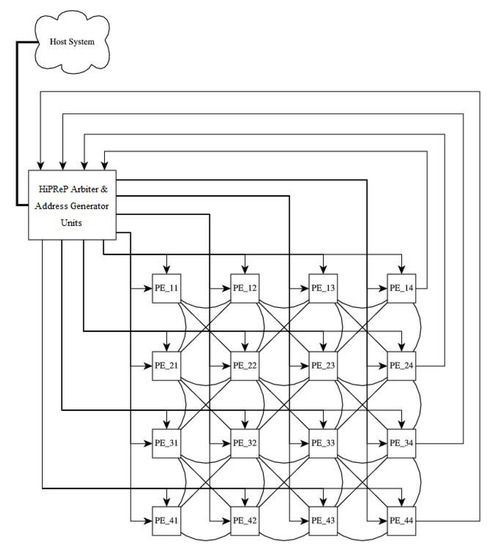
Figure 1.
HiPReP CGRA instance with PE array.
By setting one or more bits in this mask, values from memory can be sent to individual PEs or broadcast to a PE subset or to all PEs on a long-line. Using a mask with several bits set synchronizes the addressed PEs, i.e., all PEs must consume the values (by reading input registers or as explained below) before the next value is broadcast. The PEs on the eastern side of the array are connected to Store-AGUs (four Store AGUs in the CGRA of Figure 1).
The AGU configuration store stores up to 10 parameter sets, which are executed one after another. This allows to change access patterns in different phases of an algorithm. e.g., it is possible to load scalar live-in variables from main memory or save scalar live-out variables to main memory by using AGU configurations with parameter , which only read or write one word. Note that all internal and external connections are synchronized by handshake signals. Hence, the operations stall automatically and dynamically if a slow computation or slow memory access occurs.
In addition to the AGUs, standard load-store units could easily be added to some PEs, thus, allowing addressed load-store, if demanded by algorithms.
The HiPReP Arbiter combines and arbitrates the memory accesses. By assigning one or several AGU interfaces to a memory channel, HiPReP can be adjusted very flexibly to different memory systems. We currently extend the Chisel model with a tightly-coupled host processor [35] where each memory channel is connected to its own L1 data cache (separate for reading and writing) integrated in the host processor’s memory hierarchy. In the subsequent examples, the fastest memory connection is assumed, i.e., each AGU is connected to its own memory channel and L1 cache. Note that, since the HiPReP kernel does not imply a fixed memory hierarchy, a loosely-coupled system where the memory channels are connected to local multi-bank SRAM (explicitly managed cache) is also feasible.
3.2. Processing Element
The HiPReP PE is a simple 32-bit processor kernel and, thus, differs considerably from usual CGRA-PEs. All operations process 32-bit wide signed integer or floating-point data. In addition to an integer ALU, each PE contains an integer multiplier, a barrel shifter (supporting logic shift-left and arithmetic shift-right) and converters between integer and floating-point numbers. For computation-intensive numerical applications, there is also a single-precision, pipelined Floating-Point Unit (FPU) with a Fused-Multiply Add (FMA) operator, which is important for efficient execution of the frequent multiply-accumulate and multiply-add instructions. The functional units of the PEs are also parameterized so that heterogeneous arrays can be synthesized and simulated as well as homogenous ones. Dividers and more complex operators are not implemented in the current HiPReP design, but these operations can be implemented by assembler macros.
Each PE has its own context memory containing a PE program with, at most, 32 instructions. These RISC-like three-address instructions are independently executed in a processor pipeline with at least three stages (or more for floating-point operations). The instructions are also 32-bit wide and support 6-bit unsigned immediate values. Increases and decreases can be implemented using the and immediate instructions.
Each PE executes its context independently, i.e., there is no global controller synchronizing the PEs. The operands are read from an internal register file (with 31 registers to and a pseudo-register providing the constant zero) or from the output registers of the neighboring PEs (referred to as input registers of the receiving PE), and the results are written to an internal register or an output register. For efficient operation, register forwarding is supported.
Hence, the input and output registers implement the inter-PE communication and synchronization on HiPReP. Every value can only be read once from an input register. If it is required several times, it must first be moved to a local register. The input registers and address the horizontal and vertical long-lines, respectively, and synchronize with the Load-AGUs. Similarly, for the eastern PEs, the output register addresses the output to the Store-AGU. The remaining input and output registers are numbered – and –, respectively, and refer to the neighbor PEs starting with the eastern neighbor in clockwise order.
The synchronization of operations with varying latencies and input/output registers requires a new structural hazard detector comparable to the scoreboards used in conventional RISC processors, cf. [5]. The PE also supports comparisons, an unconditional jump () and conditional branches ( and ), which compare a register to zero. The unconditional jump never incurs a delay, and the conditional branches only incur a delay if the jump is not taken. Hence, jumping back to the start of a loop body does not incur a runtime penalty.
The special instruction implements a zero-delay infinite loop with a loop body ranging from instruction x to y. This accommodates the frequent situation that some values must be loaded once in a prologue before an infinite loop starts. If this instruction is used, the termination of the HiPReP execution must be detected by the Store-AGUs, i.e., when all generated results have been stored to memory, the execution terminates. Otherwise, the PEs terminate individually when the instruction is reached.
Note that there are no explicit routing resources (apart from the long-lines connecting to the AGUs). Hence, routing has to be realized by instructions from an input to an output register in a PE’s context memory as part of the executing PE program.
4. CHiPReP Design and Implementation
The Compiler for HiPReP (CHiPReP) is a C Compiler, which maps inner loops annotated with a pragma to HiPReP. It is based on the CCF tool [31] (github.com/MPSLab-ASU/ccf, accessed on 21 October 2021), which, in turn, is based on the LLVM compiler framework [36]. CCF is a co-design compiler that generates combined excutables containing host processor code and CGRA code. The host processor code is transformed such that scalar live-in variables processed by the CGRA are stored in global variables by the host processor, and live-out variables are stored by the CGRA in global variables. CCF does not support streamed load-store.
In contrast to CCF, CHiPReP currently only generates CGRA (HiPReP) executables since we do not yet have a co-simulator. We plan to utilize CCF’s co-design capabilities to simulate an entire system in future work. Nevertheless, live-in and live-out variables and streamed load/store of array data is supported.
Figure 2 shows the overall compilation flow. The top part contains the compiler passes directly integrated in LLVM. The remaining three passes (CMM, Assembler and AGUG) are implemented independently of LLVM and work on graph representations of the loops mapped to HiPReP. The blue and yellow blocks were implemented in this project, and the turquoise block DDGGen was adjusted from CCF.
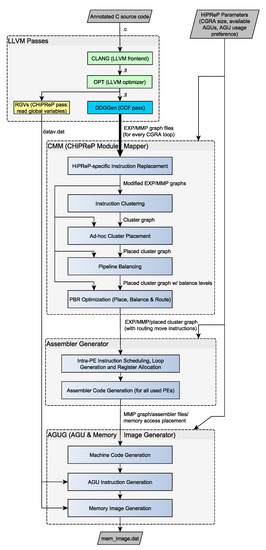
Figure 2.
CHiPReP Compilation Flow.
The next sections describe these passes in detail. Note that some of the presented algorithms are simplified for the sake of clarity. We use the C progam shown in Listing 1 as running example. It is a simple box filter (a two-dimensional convolution using a window [37]) on integer images. A box filter computes a target image pixel by taking the average of the source pixel values in the filter window, in this case the pixels src[v][h], src[v][h+1], src[v+1][h] and src[v+1][h+1]. In this example, the innermost loop (after #pragma CGRA) is executed on HiPReP.
Note that CHiPReP does not implement advanced loop optimzations as loop unrolling, loop tiling, loop interchange etc. as discussed in earlier work [22,23]. These optimizations can be included in the LLVM optimizer OPT, e.g., [38] and willl be executed before the CHiPReP main passes are executed.
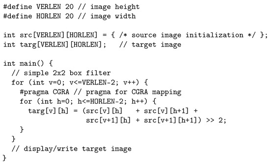

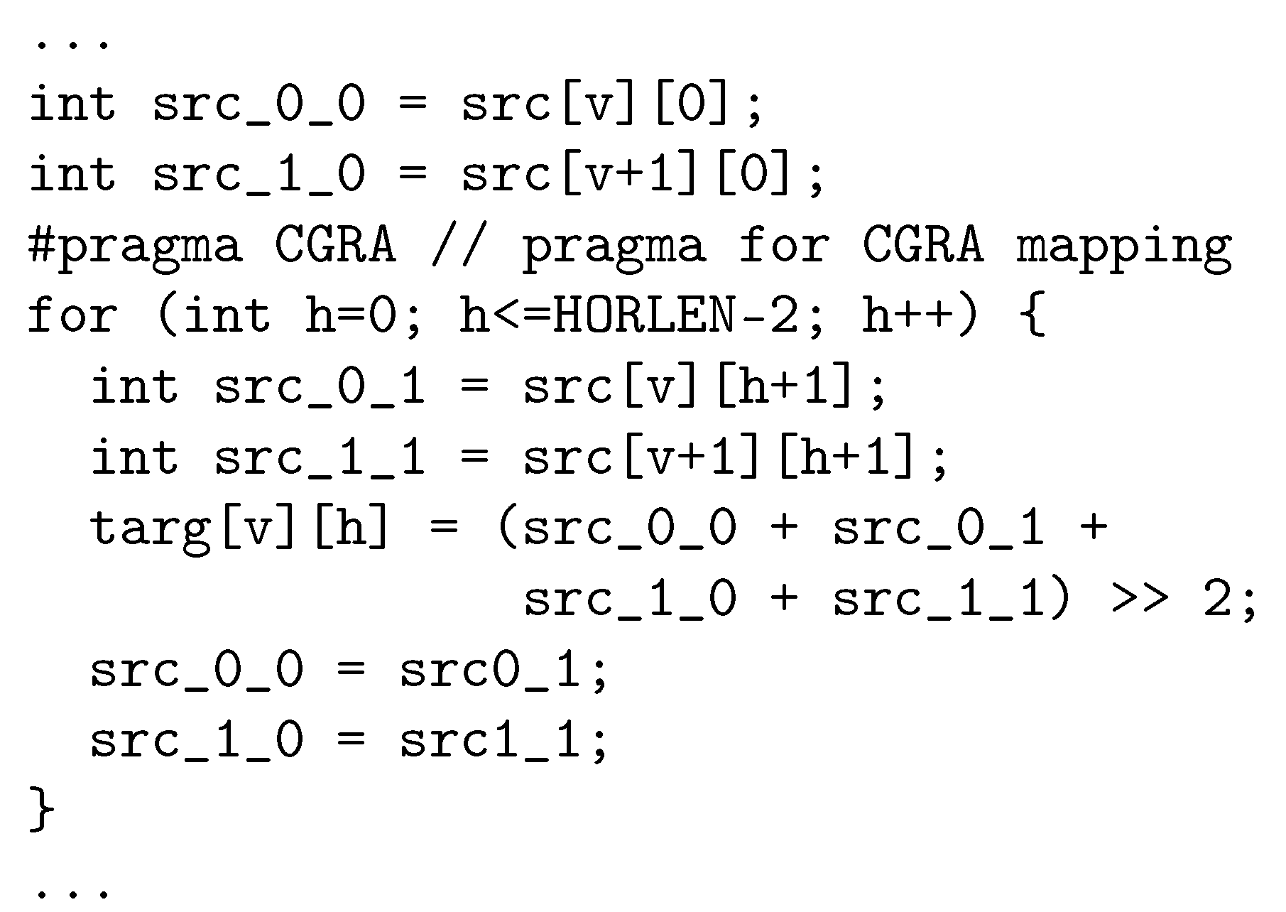
Listing 1.
Example 1: A simple 2 × 2 boxfilter program for integer images.
Listing 1.
Example 1: A simple 2 × 2 boxfilter program for integer images.
4.1. LLVM Passes
The first two LLVM passes (green boxes CLANG and OPT) in the top block of Figure 2 are standard LLVM passes, while the pass DDGGen is an extended version based on a CCF pass. The auxiliary pass RGVs was newly developed for use with the standalone HiPReP simulator.
4.1.1. LLVM Frontend: CLANG
First, the input program is parsed by the LLVM frontend CLANG. It contains a standard-compliant C parser and semantic analyzer that generate the program’s LLVM Intermediate Representation (IR), which is stored as a readable text file in the .ll format.
4.1.2. LLVM Optimizer: OPT
Next, the program is processed by the LLVM optimizer OPT. OPT implements a large set of machine-independent standard optimizations comparable to GCC (gcc.gnu.org, accessed on 21 October 2021). In CHiPReP, OPT parameters to perform several loop normalizations and transformations are used, e.g., array accesses are optimized such that values reused in the next inner loop iteration do not have to be read from memory again. Effectively, the inner loop of the boxfilter program (Listing 1) is replaced by the loop in Listing 2. (For clarity, we do not show the internal representation but the corresponding C source code.) Note that the transformed loop only requires two memory read accesses per iteration, one for each accessed source image row. However, the newly generated variables src_0_0 and src_1_0 have to be set to the first pixels of the two rows before the inner loop and set to the newly read values within the loop.
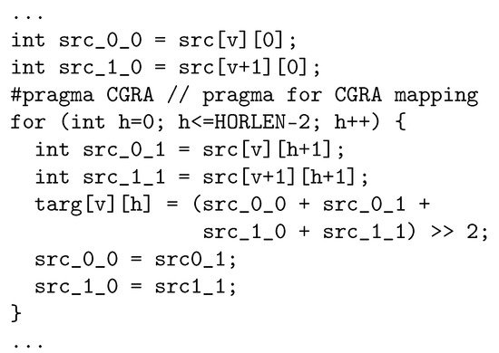
Listing 2.
Example 1: Boxfilter’s inner loop after input–reuse transformation.
Listing 2.
Example 1: Boxfilter’s inner loop after input–reuse transformation.
4.1.3. Data Dependence Graph Generation: DDGGen
The next pass, DDGGen (Data Dependence Graph Generation), actually is an additional transformation, which is dynamically loaded to a second call of the LLVM OPT pass. It is based on CCF’s DDGGen pass and was extended to handle accesses to one- and two-dimensional arrays using HiPReP’s AGUs. DDGGen scans the source code for #pragma CGRA annotations. For all innermost loops preceded by this pragma, the live-in and live-out variables are discovered and directed Data Dependence Graphs (DDGs) are generated in separate directories for every loop. If the loop cannot be mapped to HiPReP, a warning for the user is printed.
This is the case if the loop body contains function calls, pointer accesses or non-linear array accesses. The graphs are stored in text files containing node and edge lists independent of the LLVM IR. Additionally, the graphs are stored as .dot files, which can be displayed using the GraphViz tool [39] (www.graphviz.org, accessed on 21 October 2021) for debugging and illustration. Figure 3 shows the DDG generated from the annotated loop in Listing 2. The nodes represent the loop’s instructions and the edges represent data dependences between the nodes. The distinction between the MMP part and the EXP part of the graph is explained in the next paragraph below.
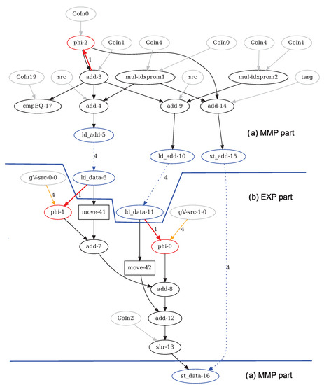
Figure 3.
Example 1: Boxfilter’s Data Dependence Graph (as generated by DDDGen), with separated (a) MMP and (b) EXP parts.
The graph contains the following components [31]:
- Arithmetic and logic instruction nodes are represented by black ovals filled with the opcode and node numbers, and constant inputs are represented by grey ovals named Co.... The edges between these nodes represent direct dataflow from source to target.
- The same holds for the move nodes (black rectangles), which only copy data. They are not functionally required, but are inserted to enable correct pipeline balancing as is explained in Section 4.2.4.
- The red phi nodes represent the phi functions inserted by LLVM because it uses static single assignment (SSA) form [40]. The red edges entering phi nodes represent loop-carried dependences, with the edge weight equal to the dependence distance.
- Nodes named by array names (src and targ in the example) represent the arrays’ base addresses.
- Source and sink nodes named gV... represent global variables used for live-in and live-out variables as explained above. The yellow input or output edges are labeled with the alignment of the memory access (always 4 = 32 bit for HiPReP).
- The blue ovals represent load and store accesses as discussed in the next paragraph.
- Conditional assignments are mapped to three-input instructions (not occurring in Example 1), which act as multiplexers, see Section 2.2.2. A boolean control input decides which of two data inputs are forwarded to the output. Conditional blocks that cannot be mapped to nodes cannot be handled by DDDGen.
DDG Splitting Algorithm As the CGRA targeted by CCF uses addressed load-store, the entire loop body (i.e., the entire DDG) is mapped to that CGRA’s PEs. In contrast to this, HiPReP uses streamed load-store. Therefore, the DDG is split in two parts: the EXecution Part EXP mapped to the PE array and the Memory Movement Part MMP mapped to the AGUs. Two additional graphs are generated for each loop, EXP and MMP. The MMP graph contains load and store operations including the counters, incrementers and offsets required for the AGU instructions.
For the boxfilter example, the MMP graph contains the upper part of the graph as well as the load and store nodes, and the EXP part contains the nodes between or live-in nodes and live-out nodes or (excluding) nodes in the lower part of Figure 3. The dotted lines connecting with or with nodes represent memory loads and stores, respectively. The edge labels (always 4 for HiPReP) indicate that four byte values are loaded or stored. The and nodes in the MMP graph are connected to the address generation expressions, and the corresponding and nodes generate or consume the memory data being accessed. The special nodes named mul-idxprom... only occur in the MMP part and are derived from LLVM array access operators.
DDGGen uses the algorithm described in pseudo-code in Figure 4 to annotate the DDG’s nodes as MMP nodes or EXP nodes. This information is then used to generate the graphs for the MMP and the EXP part.
Figure 4.
DDG Splitting Algorithm Split_DFG.
The algorithm annotates DDG nodes as belonging to the EXP or MMP part by recursively traversing the DDG starting from the outputs up to the nodes (for the EXP part) or starting from the and nodes (for the MMP part). Note that some nodes can be annotated as belonging to both the EXP and the MMP par—e.g., this is the case if the loop variable (represented by a phi node) is used both for array address generation and for computing values in the EXP part.
4.1.4. LLVM Pass RGVs
The auxiliary LLVM transformation RGVs (Read Global Variables) is only required as long as there is no co-simulator available for HiPReP. It generates a text file datav.dat, which contains the names, sizes and initialization values of the global variables. These values are included in the memory image used by the HiPReP standalone simulator (see Section 4.4.3) and allows limited loop testing without co-simulating the host processor.
4.2. CHiPReP Module Mapper: CMM
The CHiPReP Module Mapper (CMM) allocates the EXP-DDG nodes to PEs and places them on the PE array. In the following, we refer to the EXP-DDG as the loop dataflow graph (DFG), as opposed to the MMP-DDG, which handles the memory accesses.
As a first step, some combinations of CCF instructions are replaced by complex HiPReP-specific instructions, see Section 4.2.1. Then, the actual mapping to PEs takes place. In simple cases, where a small DFG is mapped to a large CGRA, an approach as for a single-context CGRA [10] could be used: Each operation is mapped to its own PE, which executes the DFG as a pipeline. Since HiPReP PEs execute PE programs, in this case, every PE repeatedly executes the same instruction in an infinite loop.
However, in most cases, a more complex approach is required as several instructions need to be combined in one PE for space reasons or to increase PE utilization. Since the overall DFG is excuted in a pipelined fashion in this case as well, these instruction combinations have to be scheduled according to their internal and external data dependencies and are also repeated for each loop iteration, see Section 4.3.1. Hence, all PEs execute short loops, which together execute the C program’s annotated loop. The execution of the PE contexts are scheduled dynamically by the AGUs and the data read from and written to neighboring PEs.
An instruction clustering method that combines the instructions mapped to one PE was developed for the DFG, see Section 4.2.2. It generates small, independent programs for each PE, which tightly interact with their neighbor PEs. Furthermore, the AGU instructions must be generated and placed accordingly to interact with the PEs, see Section 4.4.2.
Before it maps a loop, CMM reads the following parameters of the given HiPReP instance:
- Number of PEs in X- and Y-direction (i.e., the array dimensions and )
- AGU availability: Apart from the default setting (all AGUs available as described in Section 3.1), instances with a restricted number of AGUs are supported. It is possible to restrict the usage to the Load-AGUs connected to either the horizontal or the vertical long-lines, or to use only every other AGU (for Load-AGUs and/or Store-AGUs).
- AGU usage preference: Selects whether nodes with several connected outputs (as in Example 1) (a) should—if possible—be connected to one Load-AGU or (b) if they should be distributed to several Load-AGUs. Option (a) is more effective for explicitly managed local memory (cf. Section 3.1) because explicitly copying input data to several local memories is slow. On the other hand, option (b) is feasible if the AGUs are connected to L1 caches since a fast L1–L2 cache interface is assumed, which makes loading several copies to several L1 caches relatively fast.
CMM also performs a combined optimization for cluster placement, pipeline balancing and routing as detailed in Section 4.2.5. Note that all these tasks—including clustering itself—are NP-hard combinatorial optimization problems, which are computationally intractable [20] [Chapter 36]. To make things more difficult, the partial problems depend on each other. Therefore, heuristic algorithms to find feasible solutions are devised in the following sections.
4.2.1. HiPReP-Specific Instruction Replacement
In this preprocessing step, a simple pattern matcher algorithm traverses the DFG and replaces appropriate instruction combinations by the complex floating-point instructions FMA (fused multiply-add), FMS (fused multiply-subtract) or MACC (multiply-accumulate). Note that the resulting, modified DFG contains three-input instructions that require special handling in the register allocation phase, cf. Section 4.3.1.
4.2.2. Instruction Clustering
Mapping the loop instructions (i.e., DFG nodes) to PEs has a direct influence on the schedule of the entire loop because the instructions in one PE are executed sequentially. As for the modulo scheduling methods often used for other multi-context CGRAs, the main goal of CMM is to minimize the Initialization Interval (II) of the loop body, i.e., the rate at which new loop iterations can be initialized. This maximizes the loop’s throughput. In an optimally pipelined and balanced DFG (whether implemented on an ASIC, FPGA or CGRA) where all operations execute with , every cycle a new iteration is initialized (and finalized after the pipeline is filled), i.e., the overall as well.
However, there are several reasons which restrict the achievable Minimum Initiation Interval (MII) [26]:
- Recurrences: Feedback cycles in the DFG (realized by nodes) prohibit pipelining. The length of the longest feedbeack cycle is the recurrence-constrained MII (RecMII).
- Resource conflicts: If several nodes need to share a resource (e.g., a load/store-unit or AGU or a computational resource, i.e., an operator in a PE), the maximal number of nodes sharing a resource is the resource-constrained MII (ResMII).
The overall achievable MII is therefore defined as [26]. Furthermore, an unbalanced pipeline can lead to "bubbles" in the execution reducing the or even to deadlocks, cf. Section 4.2.4.
To achieve a minimal value close to , we devised a clustering heuristic for the DFG. A clustering partitions the node set of a DFG into disjoint clusters. The clusters (which will later be mapped to PEs) are defined such that the PE utilization is evenly distributed and in turn the maximum of all PEs (which determines the overall ) is minimized. However, the routing connections cannot be considered in this phase because the clusters are not yet placed.
Nevertheless, routing requires nodes, which increase a PE’s . Therefore, the heuristic also attempts to minimize the number of connections to other PEs. The method has some similarities with the Function Folding approach [28] developed for the PACT XPP CGRA but attempts to find the smallest for each loop, while, in [28], a fixed is given by the hardware architecture.
In the first processing step, DFG nodes forming a Strongly-Connected Component (SCC) are detected using Tarjan’s algorithm [20] (Section 23.5) and are combined in one cluster because distributing nodes in a cycle on several PEs would increase since moving values between PEs adds additional delays. Only if the number of instructions available in the PE’s context memory is exceeded, are several PEs used.
Then, a new cluster is allocated for every remaining node, resulting in an initial clustering C, which may be infeasible because the number of clusters is larger than the number of PEs in the given HiPReP instance.
Clustering HeuristicFigure 5 describes the clustering heurisic. The algorithm assumes a homogenous PE array, i.e., all instructions can be mapped to all PEs. For inhomogenous CGRAs, this algorithm and the subsequent placement method could be adjusted to the restricted mapping options.
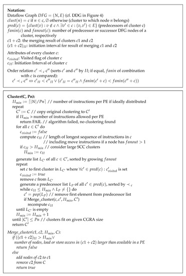
Figure 5.
Clustering Heuristic Cluster.
The heuristic uses the initial clustering C and the number of available PEs as inputs. Note that C inherits the predecessor relation from the underlying DFG (see Notation in the figure). As the DFG cycles are mapped to single clusters, the resulting cluster graph C is a directed acyclic graph (DAG). If this is not the case because a cycle had to be split over several clusters, these clusters have to be treated as one larger cluster in this algorithm. The result of the algorithm is an optimized clustering (i.e., cluster graph) with minimal and , i.e., with enough PEs for all clusters.
First, the algorithm determines , the resulting from an even distribution of all instructions on the available PEs. Then, is computed for all clusters c (normally 1). Only for SCCs, is increased accordingly. The outer repeat-loop attempts to find a clustering with . This loop is repeated with increasing values for until a clustering is found.
As the number of inter-PE connections must be as small as possible, only clusters with connected nodes (i.e., with data dependencies) are merged. Therefore, clusters are merged with their predecessors. The inner repeat loop traverses C topologically in a top-down direction and first processes clusters with small fanout (in the order of the list ). Small fanout values are preferred because they lead to a smaller fanout of the merged cluster if merged with a successor, e.g., if a cluster has only one successor and is merged with this successor, the resulting node does not have a larger fanout than the successor alone.
For the selected node c, a list of predecessors is generated, and as many predecessors as possible are merged with c. Clusters are not merged if the resulting would be larger than or if c would require more connections to Load-AGUs or Store-AGUs than available.
Leaf nodes (only connected to memory-loads) are not changed because they have no predecessors in C (i.e., in the DFG). However, their successors are combined with these clusters to form larger clusters. Since DFGs tend to have more inputs than outputs (because expressions translate to trees in the DFG), the number of inter-PE connections can be reduced by a top-down clustering. The order relation is used to add predecessors in clusters with smaller first to the predecessor list because the chance of merging them successfully with c is larger. For clusters with the same value, the one with fewer predecessors (i.e., fanin after merging with c) is added first. This strategy reduces the number of inter-PE connections further.
Figure 6 shows the clustering results for Example 1 for two different HiPReP instances: (a) For the larger CGRA with 16 PEs, no nodes are clustered. All the clusters C1 to C8 contain one node (the node or instruction numbers are reported in parenthesis), and can be achieved for the entire CGRA. (b) For the smaller CGRA with four PEs, up to three instructions are clustered, resulting in the clusters C1, C3 and C4. Though the move nodes 41 and 42 can be removed in this case, only can be achieved as is discussed in Section 4.3.2. An even distribution of the eight clusters on four PEs would require clustering two unconnected instructions. This solution is not considered by our heurisic as it would likely lead to routing problems.
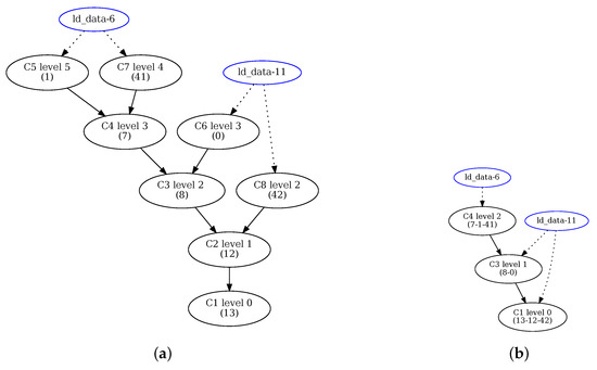
Figure 6.
Example 1: Clustergraphs (as generated by CMM) for (a) 4 × 4 PE array and (b) 2 × 2 PE array.
The nodes are not part of the cluster graphs but were added for clarity. The pipeline balancing levels of the clusters are given; see Section 4.2.4 below.
4.2.3. Ad-Hoc Cluster Placement
Next, CMM generates an ad-hoc placement P of the clusters in two steps that focuses on AGU connections and does not optimize routing connections:
- (1)
- Load/store Placement: First, clusters connected to two nodes are placed such that the values can be loaded from the two Load-AGUs connected to the PE’s horizontal and vertical long-lines. The Load-AGUs are reserved for these instructions. If a node is already mapped to a Load-AGU, it is attempted to reuse this AGU for the next cluster connected to this in order to avoid duplicating values in local memories or L1 caches. Next, clusters connected to one node are handled similarly. If a cluster is also connected to a node, it is preferably mapped to the eastern column (to avoid routing connections to the Store-AGU), and the Store-AGU is reserved. The same happens to all other clusters connected to a node.
- (2)
- Internal Node Placement: Finally, the remaining nodes are placed in top-down fashion below their predecessors if possible, or on other available PEs.
The ad-hoc placement result P of the clustergraph from Figure 6a to a 4 × 4 CGRA is displayed in Figure 7a. The black arrows represent the long-line connections to the Load-AGU and the connection to the Store-AGU. It is obvious that the inter-PE connections (light-blue arrows) are suboptimal and require additional instructions for routing. The placement resulting from the optimization discussed in Section 4.2.5 is shown in Figure 7b. The ad-hoc placement of the clustergraph from Figure 6b to a small 2 × 2 CGRA is already optimal and displayed in Figure 7c.
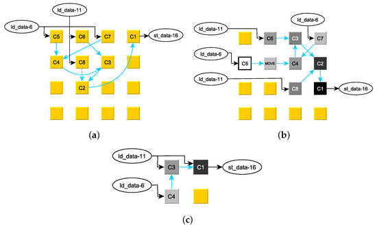
Figure 7.
Example 1 Placement: (a) ad-hoc preplacement on a 4 × 4 PE array, (b) optimized placement on a 4 × 4 PE array, and (c) placement on a 2 × 2 PE array.
4.2.4. Pipeline Balancing
As already mentioned above, the cluster graph mapped to the PE array must be balanced in order to achieve the optimal throughput, i.e., all paths from a source node (load from memory) to a target node (store to memory) must have the same number of delays or pipeline stages. On HiPReP, values are delayed by one cycle when they are stored in an output register and read by a neighboring PE, i.e., on each hop in the interconnection network.
In this phase of CMM, each cluster is assigned a balancing level. The algorithm is similar to ALAP (as late as possible) scheduling in high-level synthesis [21], see [41]. For every cluster c connected to instructions or to live-out variables, is assigned. For the remaining clusters, the levels are assigned the maximum level of their successors, incremented by one:
where
Note that, in order to minimize the number of intermediate hops required to balance the pipeline, the level of clusters which have a higher level in ASAP (as soon as possible) scheduling (i.e., movable clusters), could be adjusted. However, finding the optimal levels is also an NP-hard problem.
The computed levels are marked in the cluster graphs, see Figure 6. To achieve an ideal throughput, the number of hops between two clusters must be equal to their level difference. This requirement is fulfilled as much as possible by the simulated-annealing optimization presented in the next section. The perfect pipelining could be achieved for the optimal placements displayed in Figure 7b,c. Therefore, the mappings simulate with and . Note that the pipeline levels are illustrated by the grey values of the PEs in these illustrations: Light PEs have a higher level and darker PEs a lower level, ending with with .
However, some special cases have to be considered for balancing:
- If several instructions are connected to the same instruction, they must have the same level if they are connected to the same Load-AGU as the values are broadcast to all connected PEs (i.e., clusters) at the same time. This cannot be achieved if two paths from the instruction have different lengths and are joined. This would be, e.g., the case in Figure 3 if node move-42 was not inserted between ld_data-11 and add-12. For this reason, the move nodes were inserted. Hence, they can be clustered and placed separately as seen in Figure 6 and Figure 7. Only if the nodes are combined in one cluster as in the small 2 × 2 CGRA, is this irrelevant.
- If a phi-node—which is preloaded with a live-in value—is also connected to a instruction, the pipeline level of the phi-node’s cluster must be one higher than the other clusters connected to the instruction. This is because the pre-loaded value is read by a Load-AGU before the first value broadcast to the phi-node’s cluster and to the other clusters arrive. Hence, the pre-loaded value must be stored in an additional hop (or instruction) so that it does not disturb the pipeline. For this reason, in Figure 6 is assigned level 5 while is assigned level 4. To accommodate the levels, the optimized placement in Figure 7b has inserted a instruction (i.e., an additional hop) between and whereas is directly connected to .
4.2.5. PBR Optimization: Place, Balance and Route
The final phase of the CMM program optimizes the ad-hoc cluster placement and performs the routing. For direct-neighbor connections, the assembler generator (cf. Section 4.3.2) has to select the correct output and input registers. However, for non-neighbor connections, instructions have to be inserted. They may use PEs, which were unused thus far or add instructions to the cluster placed on a PE. Since this increases the cluster’s , the routing decisions directly influence the loop’s throughput. Furthermore, the instructions are part of the loop’s pipeline and must, therefore, also have the same pipeline level as the cluster they are added to. Otherwise, pipeline “bubbles” or even deadlocks occur.
Simulated Annealing Since placement, pipeline balancing and routing (PBR) are tightly coupled and cannot be separated, we use the well-known, generic Simulated Annealing [15,16] algorithm to optimize the cluster mapping, see Figure 8. Starting with the ad-hoc placement P, the algorithm sequentially performs “moves” in the solution space, i.e., stepwise changes in the placement of one or two clusters to PEs as explained below. Thereby, it attempts to find a globally optimal placement while avoiding local optima.
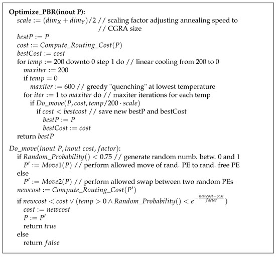
Figure 8.
Simulated Annealing algorithm Optimize_PBR.
When a move changes a cluster’s position, the reservations of the connected AGUs (if given) are also changed. Depending on the chosen AGU usage preferences, placement changes, which allocate additional Load-AGUs for the same instruction are allowed or not. For the example programs and evaluations, we allow splitting instructions over several Load-AGUs because we assume that the Load-AGUs are connected to L1 caches as discussed in Section 4.2 (item AGU Usage Preference).
The algorithm consists of two main for loops: The outer loop decreases the temperature from 200 to zero, and the inner loop attempts 200 placement moves for each temperature step (and 600 attempts for temperature zero to greedily find the best final moves). This scheme, the probabilities and factors were determined experimentally. The function attempts to randomly apply one of the following moves on placement P:
- 1
- Move 1 (75% probability) removes a cluster from its position and maps it to an unused PE.
- 2
- Move 2 (25% probability) swaps the position of two clusters.
The functions and apply these moves and return a new placement . To choose between them and to select the changed PEs, the function - is used. It returns a random number between 0 and 1. (Note that these simple functions are not elaborated in Figure 8). accepts a move if the new cost of is smaller than the old cost, i.e., if is better. For positive temperatures, even a worse solution is accepted with a small probability, which becomes smaller with lower temperature and larger increase of the cost function.
The probability is also influenced by the CGRA size through and . This probabilistic behavior of Simulated Annealing distinguishes it from simple greedy search methods, which would become trapped in a local minimum of the cost function. If the move is accepted, the input/output parameters P and are changed, and is returned. Note that the algorithm saves the best placement and cost found thus far in variables and .
The cost function is of crucial importance since it steers the Simulated Annealing process. It reflects the quality of a solution (i.e., a placement) and must be minimized. In our implementation, the function (as explained below, cf. Figure 9) performs the routing for the placement P and computes and returns the cost function. After some experimentation, we defined a cost function that combines the values (the achieved ), (the sum of all routes’ costsum values, which is higher if the throughput is decreased, as explained below in paragraph Routing) and (the accumulated length of all long routes with two or more hops).

Figure 9.
Congestion-based routing algorithm Compute_Routing_Cost.
is weighted with the large factor , and is weighted with the smaller factor . Finally, is added without a weighting factor since it is the least relevant parameter. Since is equivalent to the maximal (diagonal) route length multiplied by the number of PEs, the other parameters are practically always neglected in the comparison of two solutions if they differ in . is the second most important parameter.
Hence, a placement with higher throughput is preferred over a more compact placement with a shorter overall route length. The cost function takes into account that a route through an already used PE increases its and must be on the same pipeline level if it is added to a cluster. As explained in Section 3.2, the increases because the route is realized by a instruction from an input register to an output register in the PE program.
Routing A congestion-based router comparable to Pathfinder [17] and VPR [18] is used to find the optimal routes. For every placement move, all connections have to be routed to determine the resulting overall . This unfortunately slows the optimization down, but the annealing time is still below a second for most test cases. Runtime measurements are presented in the second Table in Section 5. We also experimented with a simple and fast approximate routing algorithm that chooses the shortest path between source and target PE of a route. However, since it greatly increases the in congested PEs, the resulting cost cannot be used to accurately assess the quality of a placement. Therefore, Simulated Annealing could not find good solutions with this fast routing algorithm.
Our router is presented in two parts: The global algorithm in Figure 9 and the router for one path in Figure 10. The global router first defines if a cluster is mapped to the PE, sets to one and to zero for all PEs. These attributes are used to assess how congested a PE is. The inner for loops of iterate over all used PEs in placement P, over all instruction nodes s (source) in that PE and over all nodes t (target), which depend on s and are placed in another PE.
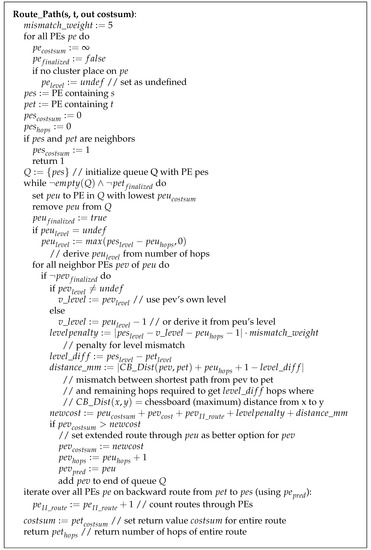
Figure 10.
Path Router Route_Path (For the notation, refer to Figure 9).
For each required route , the single path router is called. Note that we route every path separately. Combining fan-out connections will be treated in future work. returns the actually implemented number of hops, i.e., pipeline levels, and , a measure for the quality of a route. These values are accumulated in and , respectively. After all connections have been routed, , the maximum value of all PEs, is determined, and is incremented for the routing PEs, which cause congestion, i.e., which end up with a higher than the value determined by the graph clustering algorithm. After that, the cost function as explained above is computed.
The routing algorithm uses an outer repeat loop, which repeats the entire process as long as an improvement occurs. Note that the increased cost for congested PEs lead to better routing results in the next iteration. Finally, the achieved cost is returned.
The path router in Figure 10 is a maze router [19] based on Dijkstra’s algorithm [20] (Section 25.2) to find the shortest path from a single source node s to all other nodes in a given graph. We restrict the search to a single path from s to the given target node t. Instead of edge weights (to compute the shortest path), the attributes , which store the cost of the entire path from s to a given node, are used.
Similar to a breadth-first search, the algorithm operates on a queue Q, which is initialized with the source node s (more precisely, with its PE ). Note that all nodes (i.e., PEs in this context) can only occur once in a path. This is ensured by setting after it is added to the path. While Q is not empty and the target node t (i.e., its PE ) is not yet finalized, the node u (and its PE ) with the lowest costsum is extracted from Q and its flag is set. Note that for all PEs in Q, a path from to was already computed.
Next, all neighbors of are examined, i.e., the search frontier is expanded. The goal is to find an optimal path , i.e., a complete route. If is not yet finalized and (which is initialized to infinite) is higher than (the cost of the path to via ), a route from over to is added (by setting , and ). Of course, if a cheaper path to is found later, this information is overwritten.
To determine , the following values are computed first:
- : The absolute difference between the number of pipeline levels between and and the number of hops taken from to , weighted by the factor (set to 5) because this difference is more significant than the other components summed up in . Note that in an ideal route with , the number of hops corresponds to the required number of pipeline levels.
- : The mismatch between the shortest path from to and remaining hops required to achieve the requested number of pipeline levels beteen and ().
Then, is computed as the sum of (for the route ), (the congestion penalty), (the II increase due to routing), and and compared with the old value as explained above.
Finally, for all PEs in the optimal route, is incremented. Note that the complete path can be traced back from to by the attributes. After the Simulated Annealing algorithm has terminated, the routing decisions made by are finalized by adding the PE coordinates and the instructions to the clustergraph.
Eventually, CMM outputs the EXP, MMP and clustergraphs including the placement and routing information. The results of optimizing Example 1 are presented in Figure 7b,c.
4.3. Assembler Generator
The Assembler program generates the PE programs from the DFG and the clustergraph.
4.3.1. Intra-PE Instruction Scheduling, Loop Generation and Register Allocation
First, the instructions are scheduled for all used PEs: The PE programs consist of at most three phases: (a) the loop prologue (reading live-in variables, setting constant registers); (b) the loop kernel repeating the instructions in the PE’s cluster; and (c) the loop epilogue (writing live-out variables). Special care must be taken for the communication between PEs: If several values use the same nearest-neighbor connection, the values are time-multiplexed. They have to be sent and received in the correct order to avoid deadlocks or wrong results. The scheduling ensures that the instructions of all PEs (including the routing s) execute without deadlocks.
We use a simple standard register allocation method that allocates registers during the life-time of a value. For the complex three-operand instructions (, ), the register must be used for the third operand since the instructions can only address two operands and one target. The instructions are converted back to conditional assignments realized by conditional branches.
4.3.2. Assembler Code Generation
Finally, an assembler file is generated for every used PE. The instructions used in the DFG are replaced by the HiPReP mnemonics. The placement information of the neighboring PEs (i.e., their direction) is used to select the correct input and output registers for the external inputs and outputs. PEs only used for routing use the instructions. Additionally, control code for the repeated loop kernel is added. It either uses the SET_MAX_PC instruction or generates an explicit control loop as shown in the following examples.
The assembler code generated for mapping Example 1 to a 4 × 4 CGRA is very simple since no clustering occurs. As an example, Listing 3 shows the generated file PE_0_2.asm (cluster C3 in Figure 7b). The instruction SET_MAX_PC ensures that the ADD_INT instruction in line 1 is repeated infinitely. There is no prologue or epilogue.

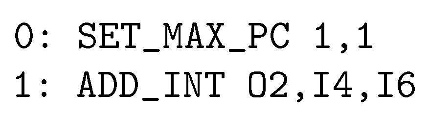
Listing 3.
Assembler code for PE 0,2 of Example 1 (C3) mapped to 4 × 4 CGRA.
Listing 3.
Assembler code for PE 0,2 of Example 1 (C3) mapped to 4 × 4 CGRA.
The result of the clustered mapping to a 2 × 2 PE are more interesting. Listing 4a shows the file PE_0_0.asm. It is a combination of the instructions phi-0 and add-8 (cluster C3 in Figure 7c). In the prologue, has to be pre-loaded with an initial value that is first sent by a Load-AGU. This is the initial value of the phi-0 instruction. Then, the loop kernel (lines 2–3) performs the instruction (i.e., input register from below is added to and sent to output register to the right) and loads the next streaming input value from . Line 0 (SET_MAX_PC) states that the loop kernel runs from line 2–3. Note that we could implement a peephole optimization that optimizes this program because lines 1 and 3 both copy a value from to . Hence, they could be removed by using directly in the instruction.
Listing 4b shows the file PE_1_0.asm. It is a combination of the instructions phi-1, add-7 and move-41 (cluster C4 in Figure 7c). Here, the loop kernel runs from lines 2–4. Note that three instructions are required since each value read from is used twice. Therefore, it has to be stored in first (line 2). Then, it is added to (line 3) and, finally, moved to (line 4). Although instruction seems to be redundant, a third instruction is required to handle the phi node correctly. This results in .

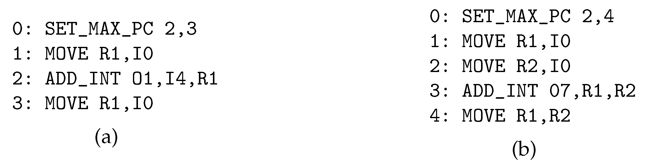
Listing 4.
Assembler code for (a) C3: PE 0,0 and (b) C4: PE 1,0 of Example 1 mapped to 2 × 2 CGRA.
Listing 4.
Assembler code for (a) C3: PE 0,0 and (b) C4: PE 1,0 of Example 1 mapped to 2 × 2 CGRA.
Both examples above do not have live-out variables. That is why the loop kernel can utilize the SET_MAX_PC instruction and execute as long as there are input values.
Figure 11a shows the quite simple Example 2, an add-reduce C program which accumulates the values of a vector. It can be mapped to a minimal 1 × 1 CGRA since it uses only one PE. It does not generate streamed outputs but only a scalar result value. Therefore, an explicit kernel loop that uses as loop counter is required in each PE. Figure 11b shows the EXP part of the DDG and (c) the generated assembler code for the only PE in this example.
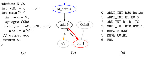
Figure 11.
Example 2: (a) Add-reduce C program, (b) EXP part of DDG and (c) assembler program.
To demonstrate where the prologue sets a constant live-in variable, the C program’s acc variable is initialized with a non-zero value (5). This results in line 1 in the assembler code. instructions with immediate sources are realized by immediate add instructions (ADDI_INT), which use the register as constant zero input. The loop kernel extends from instructions 2–4. The overhead for the explicit loop leads to . After the loop has terminated, the result is output in the program’s epilogue, which consists of line 5 and the instruction in line 6.
Since the current HiPReP implementation does not support division instructions, integer and floating-point divisions are replaced by assembler macros in the PEs. Since they contain inner loops themselves, they increase the PE’s , which must already be considered in the clustering heuristic in Section 4.2.2.
4.4. AGU and Memory Image Generator: AGUG
The AGUG program performs the final tasks of the CHiPReP compiler.
4.4.1. Machine Code Generation
First, the assembler files generated as explained above in Section 4.3 are translated to binary code. A C++ library provided by the HiPReP developer is used for this purpose. For each instruction, a 32-bit word is generated.
4.4.2. AGU Instruction Generation
Next, the AGU instructions have to be generated. They are extracted from the MMP graph (cf. Section 4.1.3) by a graph pattern matcher. It analyzes linear accesses to 1D and 2D arrays and generates instructions with the correct , , and (for Load-AGUs) values. Nested loops and more complicated accesses, which are not linear functions of the inner loop index variable currently cannot be processed, e.g., the array read access in the Example 2 introduced above is executed by the following AGU instruction (where the base address of array a is 4096):
base = 4096; count = 20; stride = 1; mask = 1.
Note that stride = 1 because the address generators always count words, i.e., in four-byte units. For the scalar live-in variables, instructions for a single-word AGU read accesses () are also generated. They are issued first. After the loop body has been processed, single-word AGU write accesses are issued for live-out variables.
4.4.3. Memory Image Generation
Finally, the AGU contexts, the binary assembler instructions for each PE and the initialization values taken from file datav.dat are combined to the memory image file mem_image.dat. For the HiPReP stand-alone simulator, the global variables are allocated to fixed addresses in main memory, which are used in the AGU contexts. The memory image is then used by the Chisel simulator for programming the HiPReP coprocessor.
5. Results
This section presents the performance results and speedup estimates achieved with CHiPReP for the standard CGRA sizes 4 × 4 and 8 × 8. Since the HiPReP-host integration is not yet implemented, the following results neglect the cache load and store times, i.e., we assume all data is readily available in L1 cache. Currently, only one inner loop execution can be simulated. Outer loops are executed by the host code.
5.1. Streaming Kernels
Table 1 shows the implementation details of streaming kernels, i.e., for loops directly operating on data vectors. The kernels compute the inner product of integer and floating-point vectors, the addition of two FP vectors and the multiplication of a FP vector with a constant value. All loops perform 100 iterations (column It) on vectors of length 100 and were mapped to a 4 × 4 HiPReP CGRA (column CGRA). For three kernels, only one PE was used for computations (column PE), while the remaining PEs are unused or only used for routing.

Table 1.
Streaming kernel results.
Only the integer inner product uses two PEs for a pipelined multiply-accumulate implementation, as the combined instruction is only available for FP numbers. Since placement is trivial for these kernels, the time in the Simulated Annealing optimization is negligible (between one and 25 ms in these cases). The following columns and show the configuration time (equivalent to the size of the configuration) and the execution time, both in cycles. (For these simulations, there are no additional pipeline stages in arithmetical operators ). Note that the configuration time can be amortized over several executions of outer loops or if no reconfiguration is required between loop executions.
Column II shows the Initiation Interval achieved by CMM. Note that the excessive cycles (i.e., are required for loading constants, setting up the loop, filling the pipeline or writing back scalar results after the loop has terminated. The inner product loops only achieve because the execution PEs have to implement a local loop with a conditional branch as explained above for Example 2, cf. Figure 11c. The other two loops can rely on the instruction and, therefore, achieve , cf. Listing 4.
Column Instr of Table 1 shows for each kernel how many LLVM instructions (generated by the CLANG and OPT passes, cf. Section 4.1) are executed in one loop iteration. Assuming similar conditions for a comparable scalar processor that executes one instruction (including load, store and branch instructions) per cycle, the ratio of Instr and II is a coarse estimate of the speedup achieved by HiPReP.
Note that these simple streaming kernels only require a fraction of the HiPReP PEs and could be replicated four times on a 4 × 4 CGRA. This results in a fourfold speedup, provided the memory bandwidth is high enough. These kernels are mainly useful for analyzing the memory performance of a complete HiPReP system.
5.2. Filter Kernels
Table 2 presents the same implementation details for one- and two-dimensional convolution filter kernels and additionally reports on the Simulated Annealing time (column ). The two-dimensional box and Gaussian filters operate on 2D arrays with 100 columns and the 1D FIR filters on vectors with 100 elements. Note that the It values are slightly shorter because some values are preloaded and the loop does not iterate over the entire index range.
Table 2.
Filter kernel results.
The box filter is the Example 1 discussed in detail in Section 4. This achieves the optimal value . The 3 × 3 Gaussian filter operates on FP values and has more operations. Therefore, implementation results are given for a larger 8 × 8 CGRA as well as a 4 × 4 CGRA. As MOVEs are combined in one PE, only can be achieved on the larger CGRA. On the smaller CGRA, more routing connections have to be combined with computing PEs so that is increased to 4.
The two versions of 8-tap FIR filters differ as follows:
- The integer version multiplies six input values with integer constants and computes the sum and shifts the result (as a normalizing division) to keep the result in range. (Two taps use the coefficient 1 and, therefore, do not require a multiplication.)
- The FP version multiplies all eight input values with fractional FP values and, therefore, does not need a final normalizing division. However, because two more multiplications are used, the overall LLVM instruction count is one more than for the integer version.
The FIR filters were also implemented on 4 × 4 and 8 × 8 CGRAs. Note that the FP version on the larger CGRA, which does not cluster any operations, uses fewer PEs than the integer version since it utilizes the combined FMA operation.
Both FIR filters achieved on the larger 8 × 8 CGRA. A smaller value is not possible since an input value from an AGU has to be distributed to two PEs (by first storing it in an internal register) in these implementations. The three s in one PE cause . On the smaller 4 × 4 CGRA, is increased to 4 for the integer version because some instructions were clustered.
There are only a few published reports on mapping similar benchmark kernels to CGRAs: (1) ([27], Table 1) reports on a 2D correlation implemented on ADRES, which is similar to the 2D convolution filters that we implemented. While , they achieved . The reasons are not explained. (2) ([24], Table 2) reports on the implementation of a FIR filter and a 2D median filter (which has a data access pattern that is also similar to 2D convolution filters) on PACT XPP. While also holds for these applications, it can be concluded from the reported loop lengths and computation cycles that FIR achieved , and the median filter achieved .
In these implementations, the value of was similar or slightly better than the values achieved by CHiPReP for HiPReP. The reason can likely be found in the underlying hardware architectures, as ADRES and PACT XPP both provide possibilities to split data streams without requiring instructions. Furthermore, both architectures only handle integer operations, and there are no comparisons of mapping the same kernel to smaller and larger CGRAs as we provide them.
The runtime of the CHiPReP compiler itself is dominated by the Simulated Annealing optimization. The last column of Table 2 reports on this Simulated Annealing time, measured in seconds. The compiler was generated using g++ -O3, and the execution times were measured on an AMD Ryzen9 5900X processor running at 3.7 GHz. Clearly, large arrays with (relatively) few used PEs lead to the longest optimization times since they offer many ”move” opportunities. The benchmarks presented in Table 2 require an acceptable optimization time between 0.1 and 1.5 s.
To summarize, the loop kernels investigated with the CHiPReP compiler achieved estimated speedup factors between 3.7 and 23.0 while using between one and 14 PEs for computations. The compiler itself runs efficiently in a few seconds on a modern processor, even for the larger CGRAs.
6. Conclusions and Future Work
This article introduced the CHiPReP compiler for the HiPReP High-Performance Reconfigurable Processor. The CMM pass with the main contributions—the DDG Splitting Algorithm, the clustering heuristic and the integrated placement, pipeline balancing and routing optimization—was presented in detail. The simulation results show that HiPReP in combination with CHiPReP is a promising accelerator for compute-intensive applications and also handles floating-point operations efficiently. The Simulated Annealing optimization algorithm did not lead to unacceptably high compilation times.
In future work, some limitations will be addressed: We will extend the CHiPReP code generation so that it handles two nested loops by exploiting the AGUs’ and parameters. Further optimizations, such as peephole optimizations on single PEs’ assembler programs, will be implemented, and an improved router using spanning trees for routes with high fanouts will be used. SCCs will be distributed over several PEs if they contain cycles that can be parallelized. Finally, a combined host and HiPReP codesign compiler based on CCF’s codesign approach will be implemented. We then plan to systematically analyze the performance of HiPReP using the PolyBench benchmark [42].
Additionally, extensions to the HiPReP architecture can improve the compilation results as follows: Conditional branches with auto-decrement could simplify the loops required when live-out variables exist, i.e., combine instructions 3 and 4 in Figure 11c. Furthermore, could be extended to a conditional branch instruction, which decrements and compares a dedicated register, thus, removing the overhead for the counting loops in a PE completely. The mapping results also show that the combination of arithmetic operations and routing often leads to a lower throughput. Hence, dedicated routing resources could improve HiPReP’s performance.
Author Contributions
Investigation, M.W. and M.M.; methodology, M.W., M.M. and P.K.; validation, M.W.; writing–original draft preparation, M.W.; writing–review and editing, M.W., M.M. and P.K. All authors have read and agreed to the published version of the manuscript.
Funding
This work was supported by the German Research Foundation (Deutsche Forschungsgemeinschaft)—283321772.
Institutional Review Board Statement
Not applicable.
Informed Consent Statement
Not applicable.
Conflicts of Interest
The authors declare no conflict of interest.
Abbreviations
| AGU | Address-Generator Unit |
| ALAP | As Late As Possible |
| ALU | Arithmetic Logic Unit |
| ASAP | As Soon As Possible |
| CCF | CGRA Compiler Framework |
| CGRA | Coarse-Grained Reconfigurable Array |
| CHiPReP | C Compiler for HiPReP |
| CMM | CHiPReP Module Mapper |
| DAG | Directed Acyclic Graph |
| DDG | Data Dependence Graph |
| DDGGen | Data Dependence Graph Generation |
| DFG | Dataflow Graph |
| EXP | Execution Part |
| FIR | Finite Impulse Response |
| FMA | Fused Multiply-Add |
| FP | Floating-Point |
| FPGA | Field-Programmable Gate Array |
| FPU | Floating-Point Unit |
| FU | Functional Unit |
| HiPReP | High-Performance Reconfigurable Processor |
| HPC | High-Performance Computing |
| II | Initiation Interval |
| IR | Intermediate Representation |
| LLVM | Low-Level Virtual Machine |
| MII | Minimum Initiation Interval |
| MMP | Memory Movement Part |
| MRRG | Modulo Routing Resource Graph |
| PE | Processing Element |
| P&R | Placement and Routing |
| SCC | Strongly-Connected Component |
| SSA | Static Single Assignment |
| VLIW | Very Long Instruction Word |
References
- Esmaeilzadeh, H.; Blem, E.; Amant, R.S.; Sankaralingam, K.; Burger, D. Dark silicon and the end of multicore scaling. In Proceedings of the 38th Annual International Symposium on Computer Architecture (ISCA), San Jose, CA, USA, 4–8 June 2011; pp. 365–376. [Google Scholar]
- Tatas, K.; Siozios, K.; Soudris, D. A Survey of Existing Fine-Grain Reconfigurable Architectures and CAD tools. In Fine- and Coarse-Grain Reconfigurable Computing; Vassiliadis, S., Soudris, D., Eds.; Springer: Berlin/Heidelberg, Germany, 2007; Chapter 1; pp. 3–87. [Google Scholar]
- Theodoridis, G.; Soudris, D.; Vassiliadis, S. A Survey of Coarse-Grain Reconfigurable Architectures and CAD Tools. In Fine- and Coarse-Grain Reconfigurable Computing; Vassiliadis, S., Soudris, D., Eds.; Springer: Berlin/Heidelberg, Germany, 2007; Chapter 2; pp. 89–149. [Google Scholar]
- Käsgen, P.S.; Weinhardt, M.; Hochberger, C. A coarse-grained reconfigurable array for high-performance computing applications. In Proceedings of the International Conference on Reconfigurable Computing and FPGAs (ReConFig), Cancun, Mexico, 9–11 December 2019; IEEE: Piscataway, NJ, USA, 2019. [Google Scholar]
- Käsgen, P.S.; Weinhardt, M.; Hochberger, C. Dynamic scheduling of pipelined functional units in coarse-grained reconfigurable array elements. In Proceedings of the International Conference on Architecture of Computing Systems (ARCS), Copenhagen, Denmark, 20–23 May 2019; Springer: Berlin/Heidelberg, Germany, 2019; pp. 156–167. [Google Scholar]
- Käsgen, P.S.; Messelka, M.; Weinhardt, M. HiPReP: High-Performance Reconfigurable Processor—Architecture and Compiler. In Proceedings of the International Conference on Field-Programmable Logic and Applications (FPL), Dresden, Germany, 30 August 2021–3 September 2021. [Google Scholar]
- Hartenstein, R. Coarse Grain Reconfigurable Architectures. In Asia and South Pacific Design Automation Conference (ASP-DAC) 2001, Yokohama, Japan, 2 February 2021; IEEE: Piscataway, NJ, USA, 2001; pp. 564–569. [Google Scholar]
- Liu, L.; Zhu, J.; Li, Z.; Lu, Y.; Deng, Y.; Han, J.; Yin, S.; Wei, S. A survey of coarse-grained reconfigurable architecture and design: Taxonomy, challenges, and applications. ACM Comput. Surv. 2019, 52, 1–39. [Google Scholar] [CrossRef] [Green Version]
- Podobas, A.; Sano, K.; Matsuoka, S. A Survey on Coarse-Grained Reconfigurable Architectures from a Performance Perspective. IEEE Access 2020, 8, 146719–146743. [Google Scholar] [CrossRef]
- Baumgarte, V.; Ehlers, G.; May, F.; Nückel, A.; Vorbach, M.; Weinhardt, M. PACT XPP—A Self-Reconfigurable Data Processing Architecture. J. Supercomput. 2003, 26, 167–184. [Google Scholar] [CrossRef]
- Mei, B.; Vernalde, S.; Verkest, D.; Man, H.D.; Lauwereins, R. ADRES: An Architecture with Tightly Coupled VLIW Processor and Coarse-Grained Reconfigurable Matrix. In Proceedings of the International Conference on Field-Programmable Logic and Applications, Leuven, Belgium, 1 September 2003; Springer: Berlin/Heidelberg, Germany, 2003; pp. 61–70. [Google Scholar]
- Ul-Abdin, Z.; Svensson, B. Evolution in architectures and programming methodologies of coarse-grained reconfigurable computing. Microprocess. Microsyst. 2009, 33, 161–178. [Google Scholar] [CrossRef]
- Cardoso, J.M.P.; Diniz, P.C.; Weinhardt, M. Compiling for Reconfigurable Computing: A Survey. ACM Comput. Surv. 2010, 42, 1–65. [Google Scholar] [CrossRef]
- Gokhale, M.; Stone, J.; Arnold, J.; Kalinowski, M. Stream-oriented FPGA computing in the Streams-C high level language. In Proceedings of the IEEE Symposium on FPGAs for Custom Computing Machines, Napa Valley, CA, USA, 17–19 April 2000; IEEE: Piscataway Township, NJ, USA, 2000; pp. 49–56. [Google Scholar]
- Van Laarhoven, P.J.M.; Aarts, E.H.L. Simulated Annealing: Theory and Applications; Mathematics and Its Applications; Springer: Berlin/Heidelberg, Germany, 1987; Volume 37. [Google Scholar]
- De Vicente, J.; Lanchares, J.; Hermida, R. Placement by thermodynamic simulated annealing. Phys. Lett. Sect. Gen. At. Solid State Phys. 2003, 317, 415–423. [Google Scholar] [CrossRef]
- McMurchie, L.; Ebeling, C. Pathfinder: A Negotiation-Based Performance-Driven Router for FPGAs. In Reconfigurable Computing; Morgan-Kaufmann: Burlington, MA, USA, 2008; pp. 365–381. [Google Scholar]
- Betz, V.; Rose, J. VPR: A new packing, placement and routing tool for FPGA research. In Proceedings of the International Conference on Field-Programmable Logic and Applications, London, UK, 1–3 September 1997; Springer: Berlin/Heidelberg, Germany, 1997; pp. 213–222. [Google Scholar]
- Lee, C.Y. An Algorithm for Path Connections and Its Applications. IRE Trans. Electron. Comput. 1961, EC-10, 346–365. [Google Scholar] [CrossRef] [Green Version]
- Cormen, T.H.; Leiserson, C.E.; Rivest, R.L.; Stein, C. Introduction to Algorithms; MIT Press: Cambridge, MA, USA, 1990. [Google Scholar]
- Gajski, D.D.; Dutt, N.D.; Wu, A.C.H.; Lin, S.Y.L. High-Level Synthesis: Introduction to Chip and System Design; Springer: Berlin/Heidelberg, Germany, 1991. [Google Scholar]
- Bacon, D.F.; Graham, S.L.; Sharp, O.J. Compiler Transformations for High-Performance Computing. ACM Comput. Surv. 1994, 26, 345–420. [Google Scholar] [CrossRef] [Green Version]
- Weinhardt, M.; Luk, W. Pipeline vectorization. IEEE Trans. -Comput.-Aided Des. Integr. Circuits Syst. 2001, 20, 234–248. [Google Scholar] [CrossRef] [Green Version]
- Cardoso, J.M.P.; Weinhardt, M. XPP-VC: A C Compiler with Temporal Partitioning for the PACT-XPP Architecture. In Proceedings of the International Conference on Field-Programmable Logic and Applications, Belfast, UK, 27–29 August 2002; Springer: Berlin/Heidelberg, Germany; pp. 864–874. [Google Scholar]
- Lam, M. Software pipelining: An effective scheduling technique for VLIW machines. In Proceedings of the ACM SIGPLAN 1988 conference on Programming Language design and Implementation—PLDI ’88, Atlanta, GA, USA, 20–24 June 1988; ACM Press: New York, NY, USA, 1988; Volume 23, pp. 318–328. [Google Scholar]
- Rau, B.R. Iterative Modulo Scheduling. Int. J. Parallel Program. 1996, 24, 3–64. [Google Scholar] [CrossRef] [Green Version]
- Mei, B.; Vernalde, S.; Verkest, D.; Man, H.D.; Lauwereins, R. Exploiting loop-level parallelism on coarse-grained reconfigurable architectures using modulo scheduling. IEE Prooceedings Comput. Digit. Tech. 2003, 150, 255–261. [Google Scholar] [CrossRef]
- Weinhardt, M.; Vorbach, M.; Baumgarte, V.; May, F. Using Function Folding to Improve Silicon Efficiency of Reconfigurable Arithmetic Arrays. In Proceedings of the IEEE International Conference on Field-Programmable Technology, Brisbane, QLD, Australia, 6–8 December 2004; pp. 239–246. [Google Scholar]
- Chin, S.A.; Sakamoto, N.; Rui, A.; Zhao, J.; Kim, J.H.; Hara-Azumi, Y.; Anderson, J. CGRA-ME: A unified framework for CGRA modelling and exploration. In Proceedings of the International Conference on Application-Specific Systems, Architectures and Processors, Piscataway, NJ, USA, 10–12 July 2017; pp. 184–189. [Google Scholar]
- Friedman, S.; Carroll, A.; Ebeling, C.; Essen, B.; Van Hauck, S.; Ylvisaker, B. SPR: An Architecture-Adaptive CGRA Mapping Tool. In Proceedings of the International Symposium on Field-Programmable Gate Arrays, Monterey, CA, USA, 20 September 2009; ACM Press: New York, NY, USA, 2009; pp. 191–200. [Google Scholar]
- CCF (CGRA Compiler Framework) Manual; Technical Report; MPS Lab, Arizona State University: Tempe, AZ, USA, 2018.
- Bachrach, J.; Vo, H.; Richards, B.; Lee, Y.; Waterman, A.; Avižienis, R.; Wawrzynek, J.; Asanović, K. Chisel: Constructing hardware in a Scala embedded language. In Proceedings of the Design Automation Conference (DAC), New York, NY, USA, 3–7 June 2012; pp. 1216–1225. [Google Scholar]
- Singh, H.; Lee, M.H.; Lu, G.; Kurdahi, F.J.; Bagherzadeh, N.; Chaves Filho, E.M. MorphoSys: An integrated reconfigurable system for data-parallel and computation-intensive applications. IEEE Trans. Comput. 2000, 49, 465–481. [Google Scholar] [CrossRef]
- Lee, J.; Lee, J. NP-CGRA: Extending CGRAs for Efficient Processing of Light-weight Deep Neural Networks. In Design, Automation & Test in Europe; IEEE: Piscataway, NJ, USA, 2021; pp. 1408–1413. [Google Scholar]
- Amid, A.; Biancolin, D.; Gonzalez, A.; Grubb, D.; Karandikar, S.; Liew, H.; Magyar, A.; Mao, H.; Ou, A.; Pemberton, N.; et al. Chipyard: Integrated Design, Simulation, and Implementation Framework for Custom SoCs. IEEE Micro. 2020, 40, 10–21. [Google Scholar] [CrossRef]
- The LLVM Compiler Infrastructure Project. Available online: https://llvm.org (accessed on 21 October 2021).
- Burger, W.; Burge, M.J. Digital Image Processing—An Algorithmic Introduction Using Java; Springer: Berlin/Heidelberg, Germany, 2016. [Google Scholar]
- Grosser, T.; Groesslinger, A.; Lengauer, C. POLLY — Performing polyhedral optimizations on a low-level intermediate representation. Parallel Process. Lett. 2012, 22, 1–27. [Google Scholar] [CrossRef] [Green Version]
- Ellson, J.; Gansner, E.; Koutsofios, L.; North, S.C.; Woodhull, G. Graphviz— Open Source Graph Drawing Tools. In International Symposium on Graph Drawing, Vienna, Austria, 23–26 September 2001; Springer: Berlin/Heidelberg, Germany, 2001; Volume 2265 LNCS, pp. 483–484. [Google Scholar]
- Appel, A.W. Modern Compiler Implementation in C; Cambridge University Press: Cambridge, UK, 1998. [Google Scholar]
- Bastert, O.; Matuszewski, C. Layered Drawings of Digraphs. In Drawing Graphs—Methods and Models; Springer: Berlin/Heidelberg, Germany, 2001; Chapter 5; pp. 87–120. [Google Scholar]
- Yuki, T. Understanding PolyBench/C 3.2 Kernels. In Proceedings of the Fourth International Workshop on Polyhedral Compilation Techniques, Vienna, Austria, 20–22 January 2014. [Google Scholar]
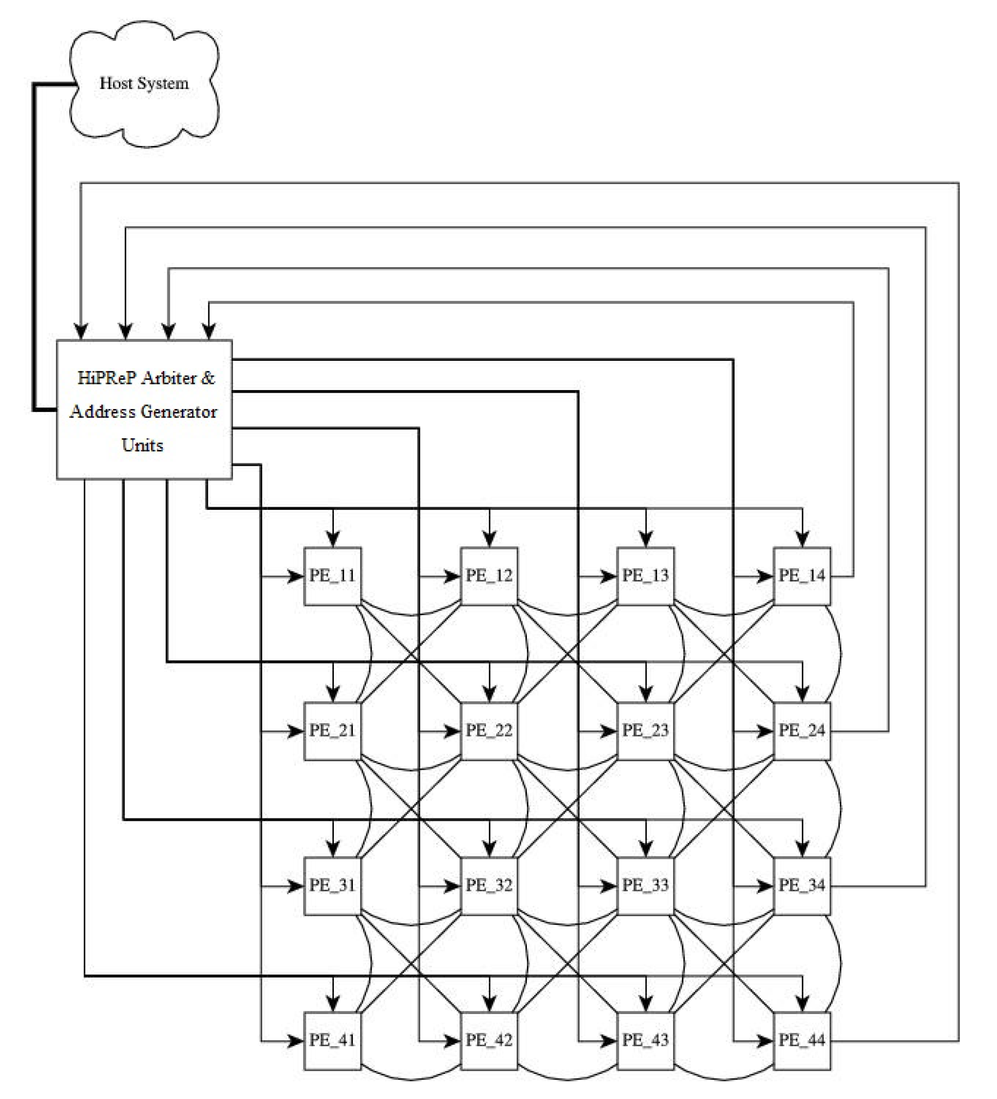
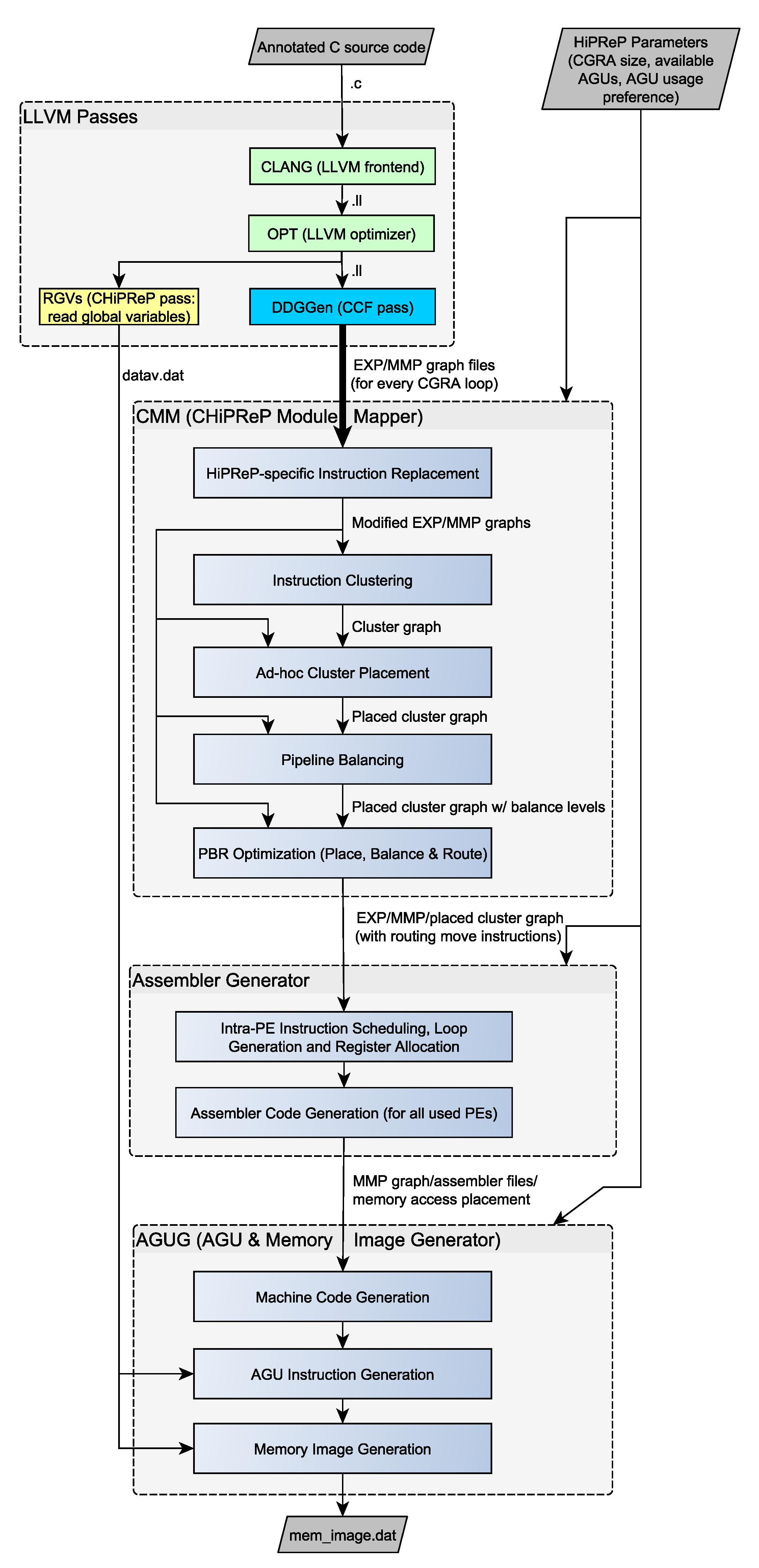
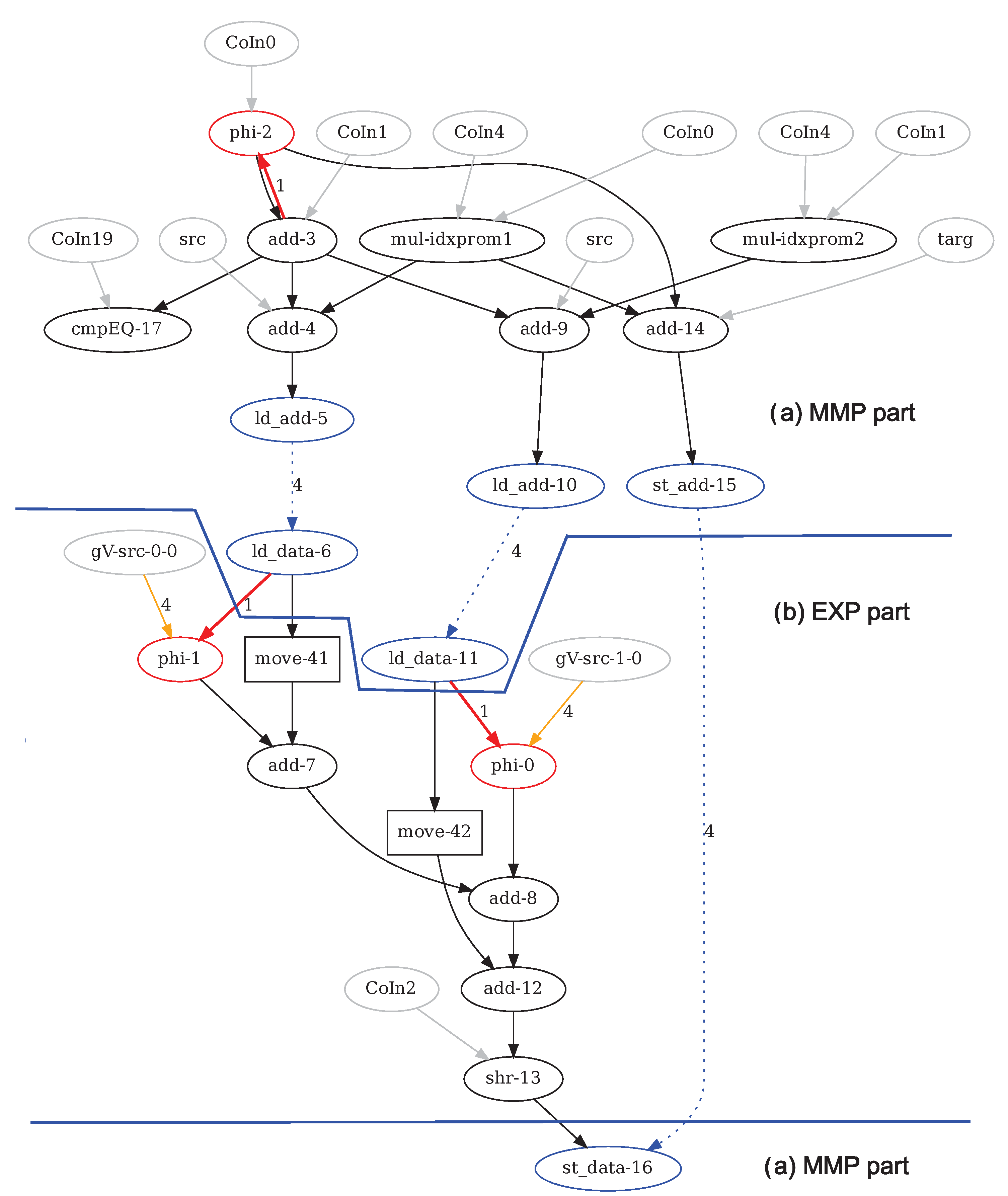

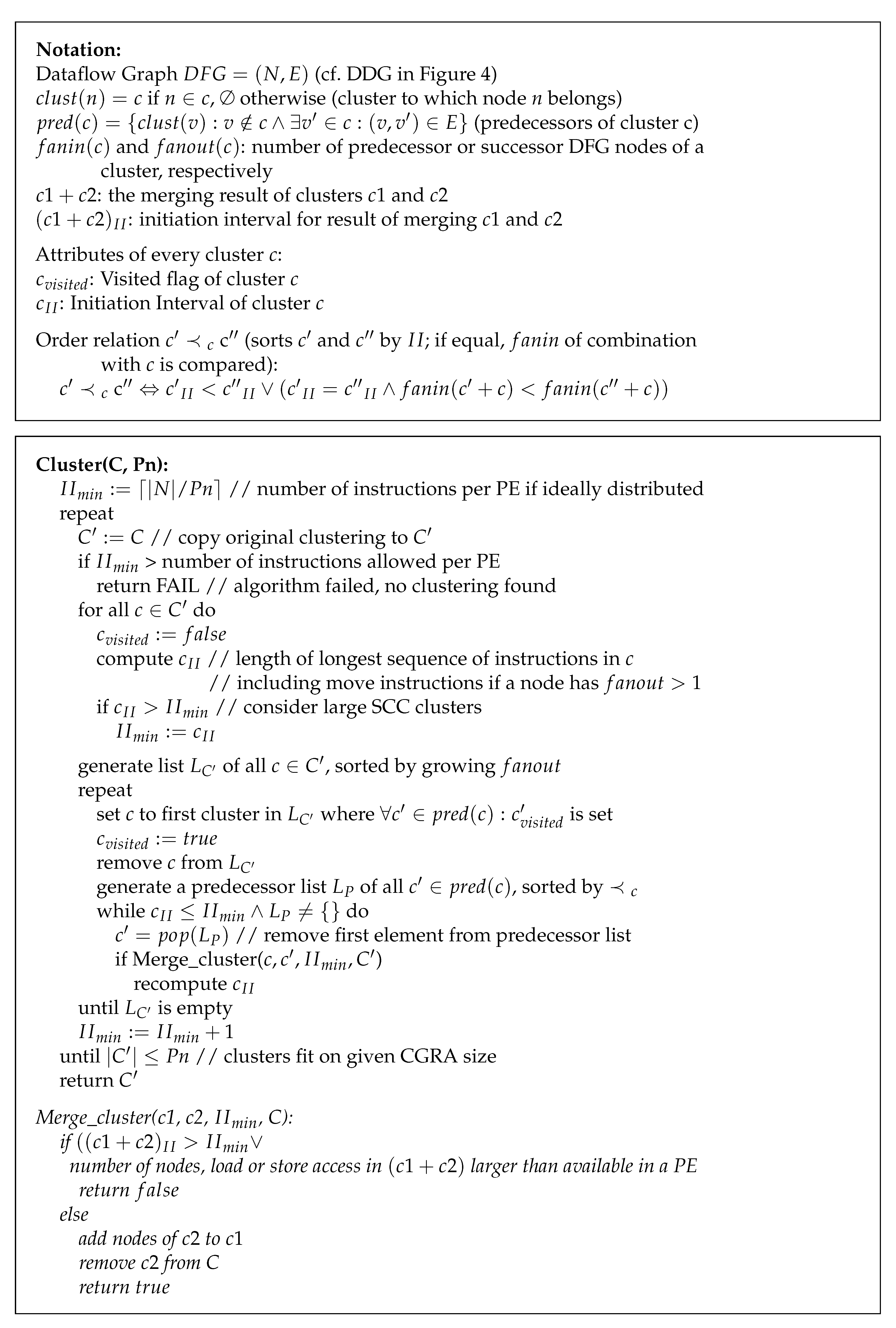

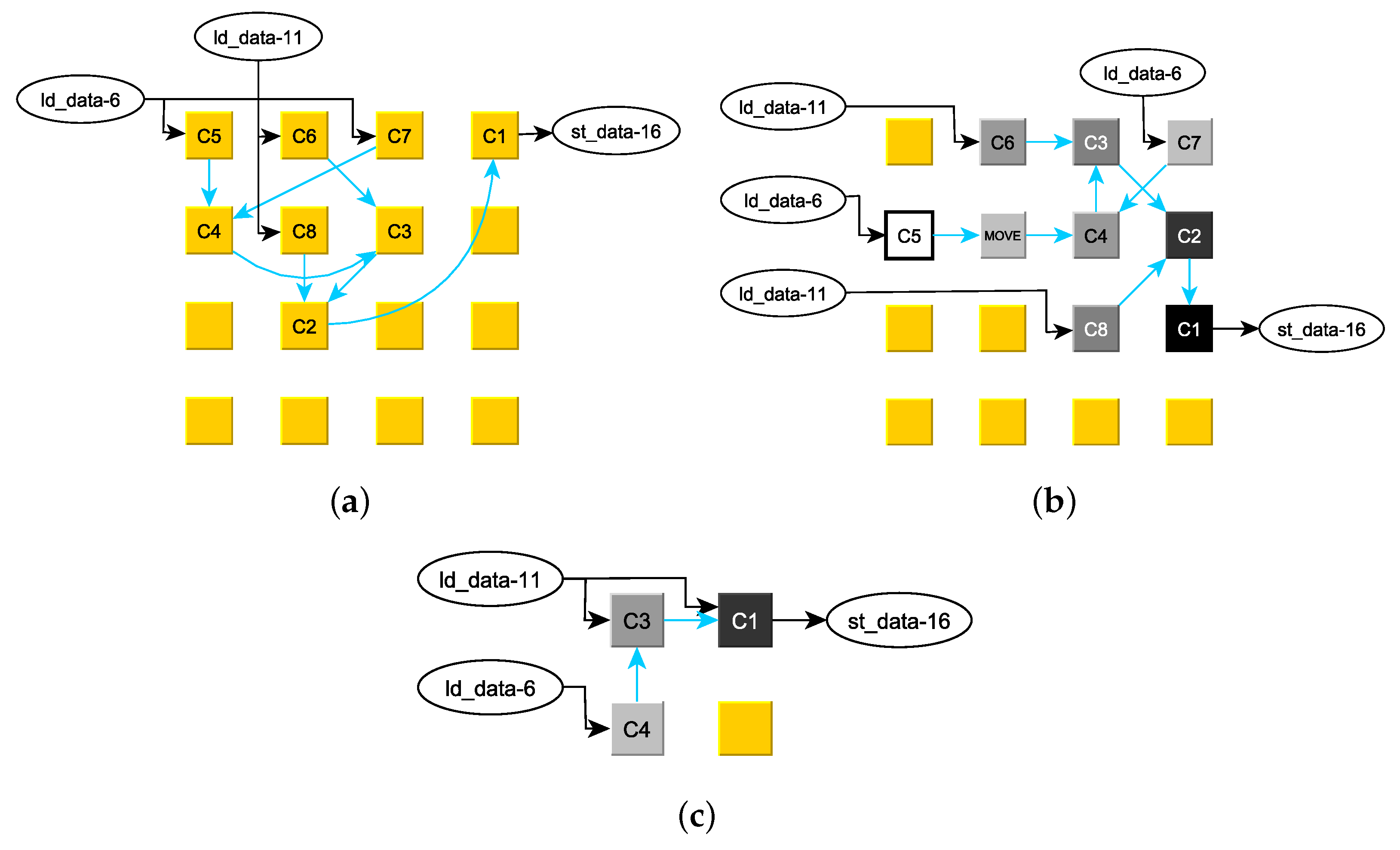

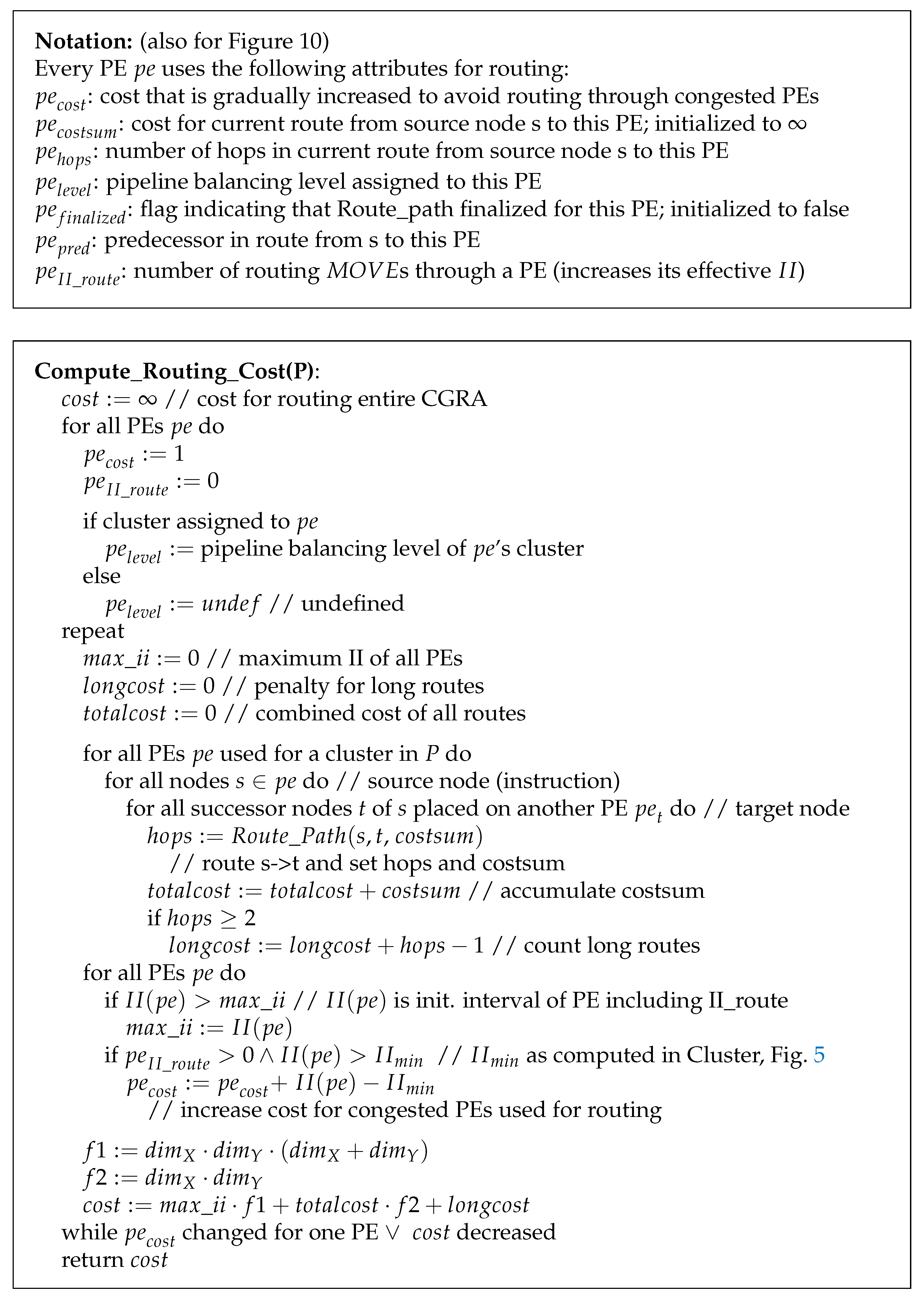
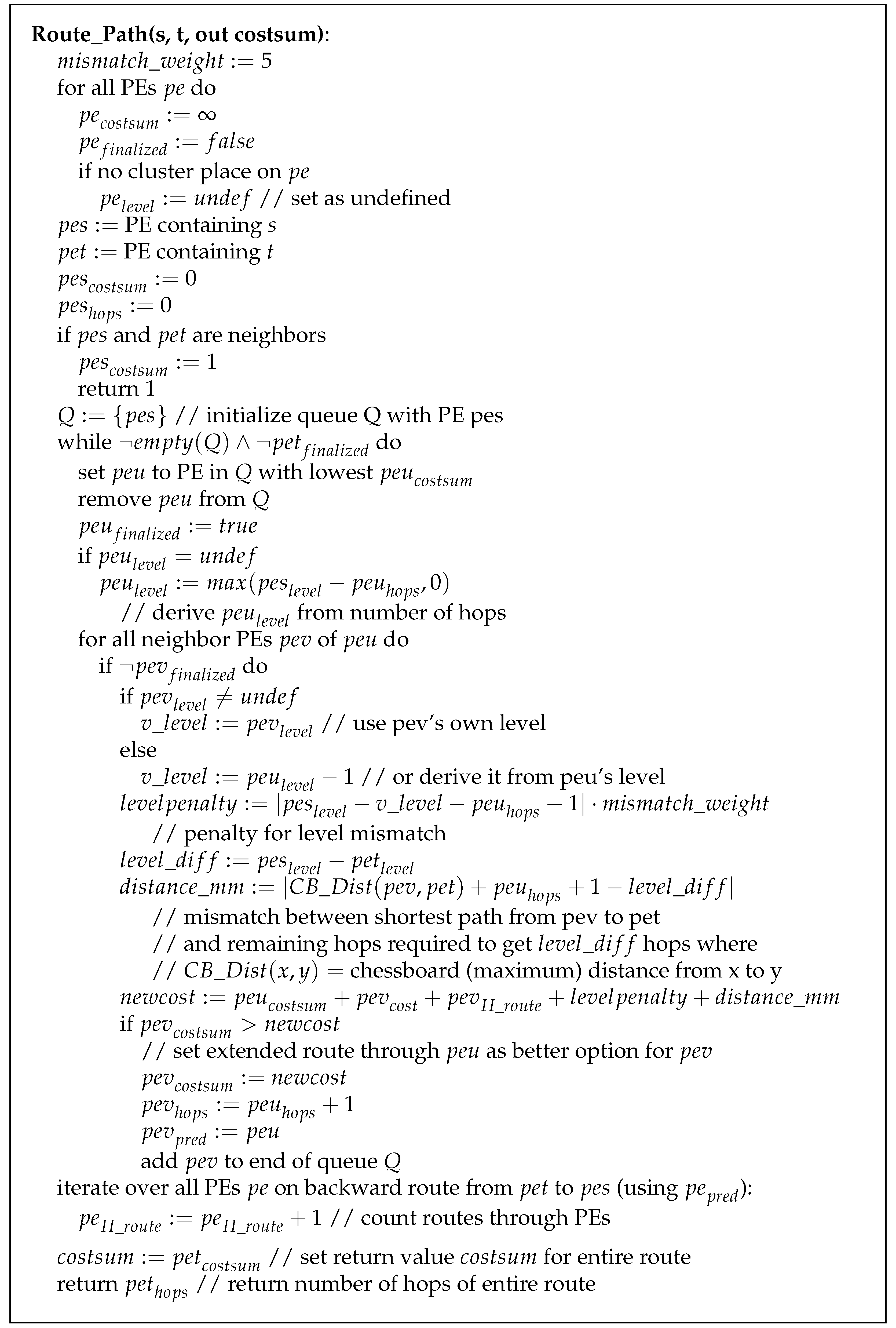
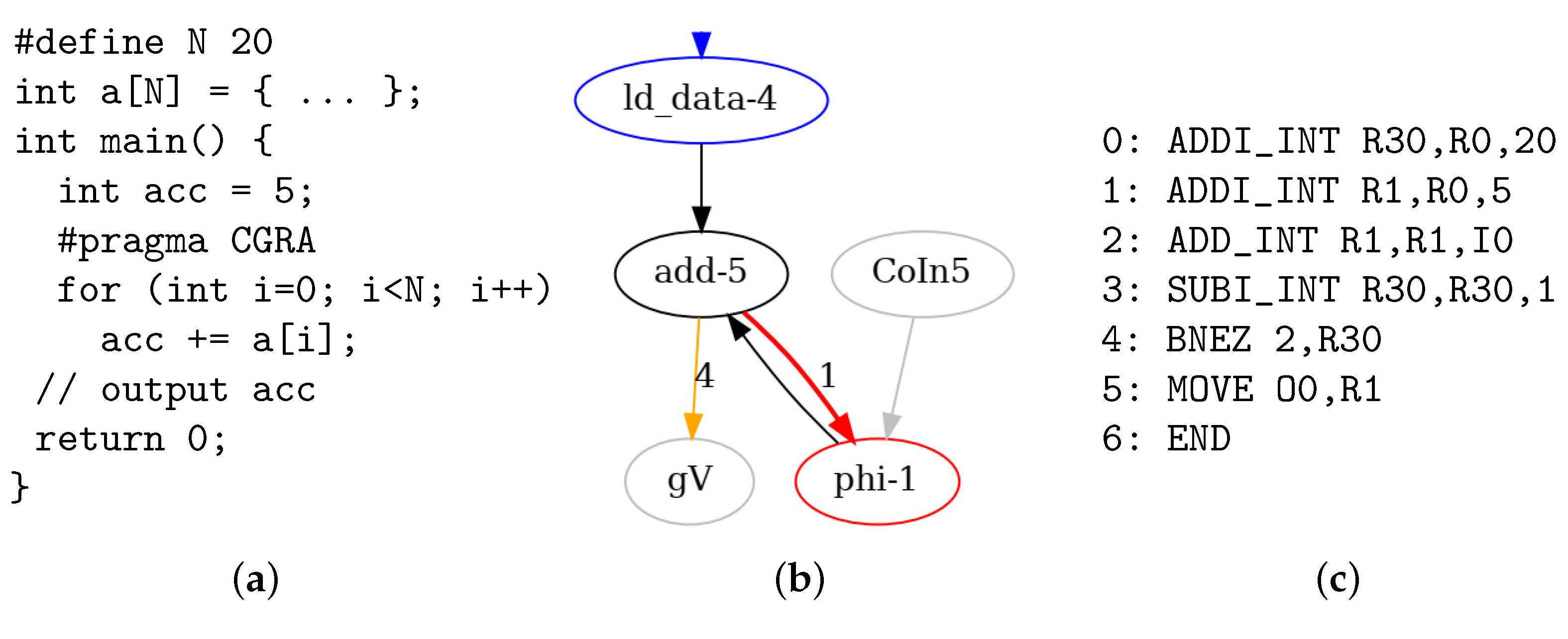
Publisher’s Note: MDPI stays neutral with regard to jurisdictional claims in published maps and institutional affiliations. |
© 2021 by the authors. Licensee MDPI, Basel, Switzerland. This article is an open access article distributed under the terms and conditions of the Creative Commons Attribution (CC BY) license (https://creativecommons.org/licenses/by/4.0/).