Abstract
This paper presents a broadband amplifier MMIC based on 0.5 µm InP double-heterojunction bipolar transistor (DHBT) technology. The proposed common-emitter amplifier contains five stages, and bias circuits are used in the matching network to obtain stable high gain in a broadband range. The measurement results demonstrate a peak gain of 19.5 dB at 146 GHz and a 3 dB bandwidth of 56–161 GHz (relative bandwidth of 96.8%). The saturation output power achieves 5.9 and 6.5 dBm at 94 and 140 GHz, respectively. The 1 dB compression output power is −4.7 dBm with an input power of −23 dBm at 94 GHz. The proposed amplifier has a compact chip size of 1.2 × 0.7 mm2, including DC and RF pads.
1. Introduction
Broadband amplifiers play an important role in high-resolution radar systems, high-data-rate communication systems, and measuring instruments. With the advancement of technology, the requirements for system performance and frequency are increasing in number, and the demand for broadband amplifiers is also increasing.
The traveling wave amplifier is common in broadband amplifier design, and is also known as a distributed amplifier (DA) [1,2,3,4,5,6]. The bandwidth, flatness, and output power of DAs are outstanding among broadband amplifiers. The main limitation of DAs is that their maximum gain does not exceed the transistor, which limits their high-frequency applications because the transistor gain is inversely proportional to the operating frequency. The cascode structure is another commonly used topology for designing broadband amplifiers, and it is often used as a basic unit to form a DA to increase its gain [3]. Because of the narrow-band characteristics of the matching network, the common-emitter (CE) structure is considered unsuitable for broadband amplifier design [7,8,9].
This paper presents a five-stage wideband common-emitter amplifier that incorporates the bias circuit into the matching network and finally obtains a maximum gain of 19.5 dB at 146 GHz with a 3 dB bandwidth of 56–161 GHz. To the best of the authors’ knowledge, the proposed common-emitter amplifier has the highest relative bandwidth (RB) in this frequency band based on the 0.5 µm InP DHBT process.
2. InP DHBT Technology
The amplifier was fabricated using a 0.5 µm InP DHBT process. The emitter contact is 500 nm wide and 5 µm long, and the base contacts are 300 nm wide at both sides of the emitter. An InGaAsP composite collector was used to eliminate the current blocking effect caused by the B-C heterojunction conduction band spike [10]. The composite collector area consists of an InGaAs setback layer, a step-graded InGaAsP layer, and a δ-doping layer; all of the layer structures are listed in [11,12]. The ft/fmax values of the transistor are 350 and 535 GHz, respectively, as shown in Figure 1. Current gain (H21), maximum available power gain (MAG), and maximum stable power gain (MSG) can be obtained by Formulas (1)–(5), where k is the stability factor. The process provides three wiring metal layers and compact interconnect vias between them. Metal-Insulator-Metal (MIM) capacitors with 0.26 fF/µm2 capacitance density and 25 Ω/square TaN TFR are also available [13,14].
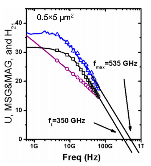
Figure 1.
The extracted ft/fmax of the 0.5 × 5 µm2 device.
Figure 2 shows a cross-section of the back end of the 0.5 µm InP DHBT MMIC process used in this paper. This process includes thin-film resistors (TFR), MIM capacitors, and three layers of interconnected metal (M1-M3). A benzocyclobutene (BCB) spin-on dielectric is used as the interlayer dielectric (ILD) with 2 µm (M1-M2) and 3 µm (M2-M3) ILD spacing between the metal layer. Electroplated Au-based interconnects are used for the metallization layers, where M1 has a thickness of 1 µm, and M2 and M3 have a thickness of 2 µm. In this design, thin-film micro-strip lines (TFMLs) can be realized with M1 as the ground and M3 as the signal line [14].
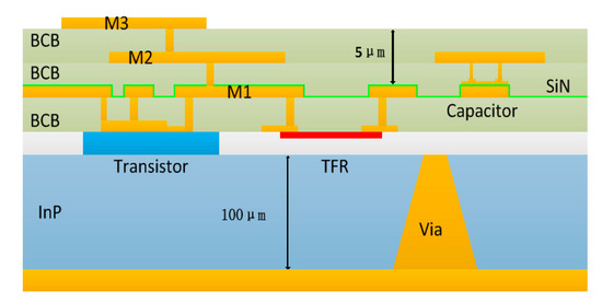
Figure 2.
Cross-sectional view of the 0.5 µm indium phosphide double-heterojunction bipolar transistor (InP DHBT) technology.
2.1. Parasitic Substrate Mode Suppression
In a multi-layer integrated circuit, thin-film microstrip lines (TFMLs) are usually used to transmit signals [15]. To achieve integration with an active circuit, a bulk substrate needs to be added under the TFML. This structure requires interlayer interconnection and, therefore, a defective structure on M1, such as a connection to transistors below the ground plane, thin-film resistors (TFRs), and series capacitors. In addition, a typical RF pad uses a coplanar ground–signal–ground (GSG) layout with ground slots. All of these ground plane fenestrations may excite the bulk substrate parasitic modes.
To eliminate the parasitic modes, it is feasible to set a number of metallized backside-vias or insert a dielectric insertion layer above the bulk substrate [16]. However, the backside via occupies a large amount of the chip area and reduces integration. The method of inserting a substrate insertion layer has a limited suppression effect on the parasitic mode, and the realization of the process is difficult.
To study the resonance phenomena caused by the parasitic modes, the HFSS model is established by taking the series capacitor as an example, as shown in Figure 3. In this model, the size of the substrate InP is 1.06 × 1 × 0.1 mm3 (l × w × h), and the size of the capacitance is 55 × 55 μm2, and the window size is 60 × 60 μm2; all conductors are made of gold.
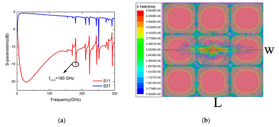
Figure 3.
Simulation S-parameters of a series capacitor with an opening window in the ground plane. (a) S-parameters of a series capacitor with an opening window in the ground plane; (b) magnitude plot of the electric field in the InP substrate observed at f3,3,0 = 180 GHz.
Mode indices of the main resonances are shown in Figure 3a. The insertion loss increases as frequency increases; simultaneously, several resonant frequencies are observed in the figure, indicating that energy is coupled into the substrate through the opening window in the ground plane. The parasitic modes bounce at the edge of the substrate due to the limited substrate volume and create resonance at certain frequencies. The resonant frequency can be approximated as:
where l, w, and h are the length, width, and height of the dielectric substrate, respectively, and m, n, and p are resonance mode indices, which are equivalent to the half-wavelength number of the corresponding dimension. The magnitude of the electric field in the InP substrate is shown in Figure 3b, where the resonant frequency is 180 GHz. It can be clearly seen that the electric field maximum distribution is equal to the mode indices (m, n, p) = (3, 3, 0), which is in agreement with f3, 3, 0 in Equation (6). Because the thickness of the chip is only 100 μm, there is no vertical resonance below 424 GHz (m, n, p = 0, 0, 1); that is, p ≡ 0 below 424 GHz.
Because the electromagnetic waves leaking into the InP dielectric substrate need to form a stable standing wave and then resonate, the addition of backside vias can prevent the generation of standing waves and eliminate resonance. Figure 4 shows a two-backside via capacitor photo and its simulation and measurement results. This backside via arrangement with the purpose of breaking standing waves can eliminate the resonance generated by the parasitic mode, and this achievement is applied to the design of the proposed amplifier.
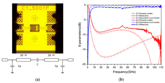
Figure 4.
(a) Capacitance photo, equivalent circuit model, and (b) S-parameters.
2.2. Equivalent Circuit Model of Capacitor
In addition to building the HFSS capacitor model, we also establish an equivalent circuit model of the capacitor to achieve accurate matching network analysis. Figure 4 shows the equivalent circuit model of the series capacitor model and its simulation results based on measurement results. This model adds two parallel capacitors Cp on the basis of the LCL model to be equivalent to the grounding capacitance caused by defects. As the defect gap spacing is constant, the parallel capacitance values in the equivalent circuit are equal. The simulation results show that the MIM capacitor density is 0.26 fF/μm2.
The comparison of S-parameters in Figure 4b shows that the equivalent circuit is consistent with the measured results, which is beneficial to the design of the matching circuit.
2.3. Equivalent Circuit Model of Transistor
The equivalent circuit model is the base of the transistor. As the frequency increases, the parasitic parameters have a significant impact on the device. Due to the use of devices of different sizes under the same process, we use the method of 3D simulation to extract parasitic parameters described in [17]. The equivalent circuit is shown in Figure 5.
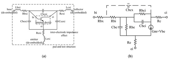
Figure 5.
Small-signal equivalent-circuit model of (a) InP DHBT and (b) the internal device [17].
Figure 5a shows the small-signal equivalent-circuit model of the device. Nine parameters are used to ensure equivalence to the inter-electrode impedance effect. The inductors and resistances of electrode contacts and posts are represented by Lbxi, Lcxi, and Lexi, and Rbxi, Rcxi, and Rexi, respectively. Figure 5b shows the simplified AgilentHBT model, which is used for the internal device equivalent circuit. The extraction method of each parameter is described in detail in [18]. Parameters biased under Vc = 1.5 V and Ib = 200 μA are extracted according to the above method and are listed in Table 1. A comparison between the model and the measured results is shown in Figure 6. The large-signal model is carried out completely in accordance with the steps in [18]; the description is not repeated here.

Table 1.
Small-signal equivalent circuit elements.
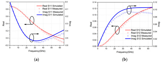
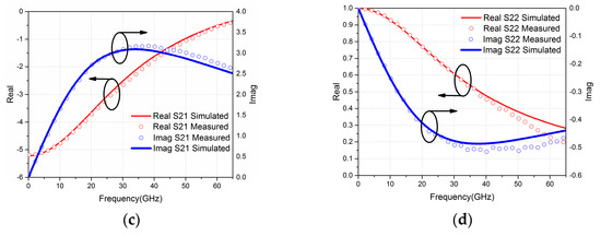
Figure 6.
Measured and simulated S-parameters of 0.5 × 5 μm InP DHBT: (a) real S11 and its image; (b) real S12 and its image; (c) real S21 and its image; (d) real S22 and its image.
3. Amplifier Design
Figure 7 shows the schematic diagram of the proposed amplifier. The amplifier adopts a five-stage cascaded CE topology, and the values of bias voltage, series resistance, and parallel capacitance of all bases are uniform; this also applies to collectors with different values. Generally, the length of the DC bias line is constant, usually λ/4 at operating frequency, and forms an open-circuit converter with the parallel capacitor. In this case, the bias circuit can be ignored in the design of the matching network. However, the electrical length of the transmission line is inversely proportional to the operating frequency; therefore, this quarter-wavelength bias circuit is only suitable for narrow-band amplifier designs.
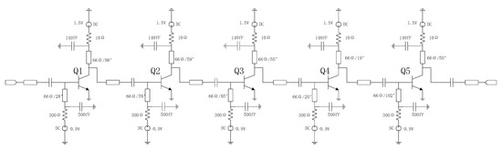
Figure 7.
Schematic diagram of the amplifier. The characteristic impedance and electrical length of the bias line are calculated at 140 GHz.
The DC bias circuit is incorporated into the matching network in this design. All bias lines have the same width, and their length is adjusted according to matching requirements.
Table 2 shows the input/output impedance and output power of each transistor derived from source-pull and load-pull simulation when the Q1 input power is −7 dBm at 140 GHz. The input power of the latter stage is the output power of the previous stage. For example, the input power of Q2, −1.39 dBm, is the output power of Q1.
Table 2.
Input/output impedance and output power of transistors.
Figure 8 compares the effect of different bias lines’ lengths on circuit performance. In Figure 8a, the input impedance Z0 = 50 Ω is the characteristic impedance of the transmission line, and the output impedance Zs1 is 18.7 − j14.3, which is the conjugate Zs of Q1. It is clear that, although a bias circuit with a λ/4 bias line (red dotted line) is theoretically equivalent to an open circuit, it is still different from a true open circuit (green dashed line). As shown in Figure 8a, the bias line we used reduces the insertion loss of the matching network above 80 GHz. The slope of the inflection point and its vicinity in Figure 8a is carefully designed, and Figure 8b shows a comparison of the maximum gain of Q1 under the matching network with different bias line lengths. It can be clearly observed that the gain is flat in the 70–95 GHz range, and this is only the boost effect of the input matching network.
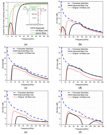
Figure 8.
Comparison of matching network insertion loss and transistor gain under different bias lines. (a) Input matching network insertion loss; (b) Q1 gain; (c) Q2 gain; (d) Q3 gain; (e) Q4 gain; (f) Q5 gain.
Adjusting the length of the bias line between Q1 and Q2, and Q2 and Q3, can reduce the loss of the matching network, thereby increasing the gain of the transistor that follows it, as shown in Figure 8c,d. The matching network between Q3 and Q4 can make the gain of Q4 stay flat above 100 GHz, as shown in Figure 8e. Because Q2 and Q3 are used to increase the gain, which affects the gain flatness of the amplifier, Q5 needs to be supplemented to balance the high gain at the 120 GHz range, as shown in Figure 8f. After the matching networks are individually designed, they are fine-tuned again in the complete circuit to obtain the best performance. Under the combined effect of multiple matching networks, the amplifier maintains a constant gain in the broadband range, as shown in Figure 9. The chip size is 1.2 × 0.7 mm2, including DC and RF pads, as shown in Figure 10.
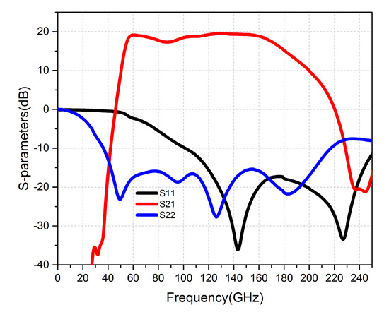
Figure 9.
Simulation S-parameters of the amplifier.
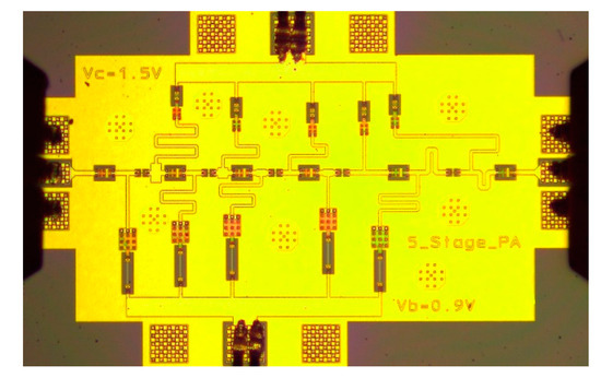
Figure 10.
Chip photograph of the amplifier MMIC. Size: 1.2 × 0.7 mm2.
4. On-Wafer Measurement Results
The on-wafer measurements were performed using a Keysight PNA-X N5247B network analyzer with Keysight N5293AX01 (0~110 GHz) frequency extenders (Keysight Technologies, Santa Rosa, CA, USA) and a Rohde & Schwarz ZVA50 network analyzer with Rohde & Schwarz ZC170 (110~170 GHz) frequency extenders (Rohde & Schwarz, Munich, Germany). The measurement results are shown in Figure 11.
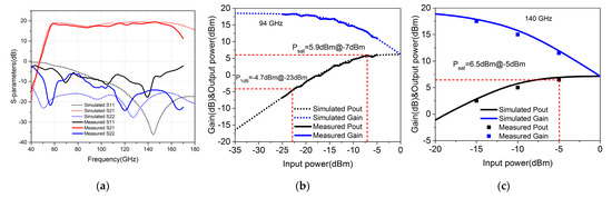
Figure 11.
Comparison of measured and simulated results. The biases for all tests are VC = 1.5 V and VB = 0.9 V. (a) Small-signal S-parameter; (b) large-signal output power and gain at 94 GHz; (c) large-signal output power and gain at 140 GHz.
The measured S-parameter results displayed in Figure 11a show that the maximum gain of the amplifier is 19.5 dB at 146 GHz, and the 3 dB bandwidth is 56~161 GHz (relative bandwidth of 96.8%). The reflection parameter S11 is below −5 dB in the range of 62~160 GHz, and S22 is below −5 dB in the range of 45~170 GHz. The amplifier provides saturation output power of 6.5 and 5.9 dBm at 94 and 140 GHz, respectively, as shown in Figure 11b,c. The 1 dB compression output power of the PA is −4.7 dBm at 94 GHz when the input power is −23 dBm. The amplifier starts to gain compression at a low input power; thus, it is more suitable for driving stages. The DC power consumption is 33.3 mW.
Table 3 shows the performance comparison of several InP HBT amplifiers. It is clear that the CE amplifier has a higher gain, while the DA bandwidth is wider. The proposed amplifier has excellent bandwidth performance compared with that of other CE cascaded amplifiers, because the DC bias circuit is incorporated into the matching network, and the bandwidth of the amplifier can be expanded by adjusting the length of the bias lines. Due to the cascaded topology, the proposed amplifier has a higher gain than that of DAs. Each transistor in this amplifier provides the highest gain and output power with minimal DC power consumption. This design has the advantages of the high gain of CE amplifiers and the wide bandwidth of DAs, but the output power is low due to the lack of power synthesis.
Table 3.
Comparison of broadband amplifiers based on the InP HBT process.
5. Conclusions
A five-stage broadband common-emitter amplifier is presented based on 0.5 µm InP DHBT technology. The measurement results show that the PA provides a maximum gain of 19.5 dB at 146 GHz with a 3 dB bandwidth of 56–161 GHz; Psat values are 5.9 and 6.5 dBm at 94 and 140 GHz, respectively. The proposed broadband amplifier is suitable for the driver stage of the broadband system.
Author Contributions
Conceptualization, W.Y. and M.Z.; methodology, W.Y.; investigation, Y.H. and Q.Y.; formal analysis, Y.H.; software, Y.H.; data curation, B.W.; writing—original draft preparation, Y.H.; writing—review and editing, W.Y.; supervision, Y.S. and W.C. All authors have read and agreed to the published version of the manuscript.
Funding
This research was funded by National Natural Science Foundation of China, grant number 61771057, and Science and Technology Innovation Action Plan of Shanghai, grant number 20590730400.
Acknowledgments
The author sincerely thank the Beijing Institute of Radio Measurement and Testing and Beijing University of Posts and Telecommunications for on-wafer testing.
Conflicts of Interest
The authors declare no conflict of interest.
References
- Nguyen, D.P.; Stameroff, A.N.; Pham, A. A 1.5–88 GHz 19.5 dBm output power triple stacked HBT InP distributed amplifier. In Proceedings of the 2017 IEEE MTT-S International Microwave Symposium (IMS), Honolulu, HI, USA, 4–9 June 2017; pp. 20–23. [Google Scholar]
- Killeen, N.S.; Nguyen, D.P.; Stameroff, A.N.; Pham, A.V.; Hurst, P.J. Design of a Wideband Bandpass Stacked HBT Distributed Amplifier in InP. In Proceedings of the 2018 IEEE International Symposium on Circuits and Systems (ISCAS), Firenze, Italy, 27–30 May 2018; pp. 1–5. [Google Scholar]
- Yoon, S.; Lee, I.; Urteaga, M.; Kim, M.; Jeon, S. A Fully-Integrated 40–222 GHz InP HBT Distributed Amplifier. IEEE Microw. Wirel. Compon. Lett. 2014, 24, 460–462. [Google Scholar] [CrossRef]
- Shivan, T.; Hossain, M.; Stoppel, I.D.; Weimann, N.; Schulz, S.; Doerner, R.; Krozer, V.; Heinrich, W. An Ultra-broadband Low-Noise Distributed Amplifier in InP DHBT Technology. In Proceedings of the 2018 48th European Microwave Conference (EuMC), London, UK, 23–27 September 2018; pp. 1209–1212. [Google Scholar]
- Shivan, T.; Hossain, M.; Doerner, R.; Johansen, T.K.; Yacoub, H.; Boppel, S.; Heinrich, W.; Krozer, V. Performance Analysis of a Low-Noise, Highly Linear Distributed Amplifier in 500-nm InP/InGaAs DHBT Technology. IEEE Trans. Microw. Theory Tech. 2019, 67, 5139–5147. [Google Scholar] [CrossRef]
- Shivan, T.; Weimann, N.; Hossain, M.; Stoppel, D.; Boppel, S.; Ostinelli, O.; Doerner, R.; Bolognesi, C.R.; Krozer, V.; Heinrich, W. A Highly Efficient Ultrawideband Traveling-Wave Amplifier in InP DHBT Technology. IEEE Microw. Wirel. Compon. Lett. 2018, 28, 1029–1031. [Google Scholar] [CrossRef]
- Griffith, Z.; Urteaga, M.; Rowell, P. A Compact 140-GHz, 150-mW High-Gain Power Amplifier MMIC in 250-nm InP HBT. IEEE Microw. Wirel. Compon. Lett. 2019, 29, 282–284. [Google Scholar] [CrossRef]
- Griffith, Z.; Urteaga, M.; Rowell, P. A 140-GHz 0.25-W PA and a 55-135 GHz 115-135 mW PA, High-Gain, Broadband Power Amplifier MMICs in 250-nm InP HBT. In Proceedings of the 2019 IEEE MTT-S International Microwave Symposium (IMS), Boston, MA, USA, 2–7 June 2019; pp. 1245–1248. [Google Scholar]
- Griffith, Z.; Urteaga, M.; Rowell, P.; Tran, L.; Brar, B. 50–250 GHz High-Gain Power Amplifier MMICs in 250-nm InP HBT. In Proceedings of the 2019 IEEE BiCMOS and Compound semiconductor Integrated Circuits and Technology Symposium (BCICTS), Monterey, CA, USA, 3–6 November 2019; pp. 1–6. [Google Scholar]
- Wei, C.; Jin, Z.; Su, Y.; Liu, X.; Xu, A.; Qi, M. Composite-Collector InGaAs/InP Double Heterostructure Bipolar Transistors with Current-Gain Cutoff Frequency of 242 GHz. Chin. Phys. Lett. 2009, 26, 038502. [Google Scholar] [CrossRef]
- Cheng, W.; Zhang, T. 0.5 μm InP DHBT technology for 100 GHz + mixed signal integrated circuits. J. Infrared Millim. Waves 2017, 36, 167–172. [Google Scholar]
- Niu, B. 0.5 μm InP /InGaAs DHBT for ultra high speed digital integrated circuit. J. Infrared Millim. Waves 2016, 35, 263–266. [Google Scholar]
- Li, O.; Zhang, Y.; Zhang, T.; Wang, L.; Xu, R.; Sun, Y.; Cheng, W.; Wang, Y.; Niu, B. 140 GHz power amplifier based on 0.5 µm composite collector InP DHBT. IEICE Electron. Express 2017, 14, 20170191. [Google Scholar] [CrossRef][Green Version]
- Yanfei, H.; Weihua, Y.; Yan, S.; Wei, C. Design of Broadband Amplifier Based on InP DHBT. In Proceedings of the 2020 IEEE MTT-S International Microwave Workshop Series on Advanced Materials and Processes for RF and THz Applications (IMWS-AMP), Suzhou, China, 29–31 July 2020; pp. 1–3. [Google Scholar]
- Eriksson, K.; Gunnarsson, S.E.; Nilsson, P.; Zirath, H. Suppression of Parasitic Substrate Modes in Multilayer Integrated Circuits. IEEE Trans. Electromagn. Compat. 2015, 57, 591–594. [Google Scholar] [CrossRef]
- Deal, W.R.; Leong, K.; Zamora, A.; Radisic, V.; Mei, X.B. Recent progress in scaling InP HEMT TMIC technology to 850 GHz. In Proceedings of the 2014 IEEE MTT-S International Microwave Symposium (IMS), Tampa, FL, USA, 1–6 June 2014; pp. 1–3. [Google Scholar]
- Chen, Y.; Zhang, Y.; Xu, Y.; Sun, Y.; Cheng, W.; Lu, H.; Xiao, F.; Xu, R. Investigation of Terahertz 3D EM Simulation on Device Modeling and A New InP HBT Dispersive Inter-Electrode Impedance Extraction Method. IEEE Access 2018, 6, 45772–45781. [Google Scholar] [CrossRef]
- Iwamoto, M.; Root, D.E.; Scott, J.B.; Cognata, A.; Asbeck, P.M.; Hughes, B.; Avanzo, D.C.D. Large-signal HBT model with improved collector transit time formulation for GaAs and InP technologies. In Proceedings of the IEEE MTT-S International Microwave Symposium Digest, Fort Worth, TX, USA, 8–13 June 2003; pp. 635–638. [Google Scholar]
Publisher’s Note: MDPI stays neutral with regard to jurisdictional claims in published maps and institutional affiliations. |
© 2021 by the authors. Licensee MDPI, Basel, Switzerland. This article is an open access article distributed under the terms and conditions of the Creative Commons Attribution (CC BY) license (https://creativecommons.org/licenses/by/4.0/).